

Chapter 3 Digitizer Basics
Understanding the Probe and Its Effects on Your Waveform
Signals travel from the tip of the probe to the input amplifier and are then digitized by the ADC. This signal path makes the probe an important electrical system component that can severely affect the accuracy of the measurement. A probe can potentially influence measured amplitude and phase, and the signal can pick up additional noise on its way to the input stage. Several types of probes are available including passive, active, and current probes.
Passive Probe
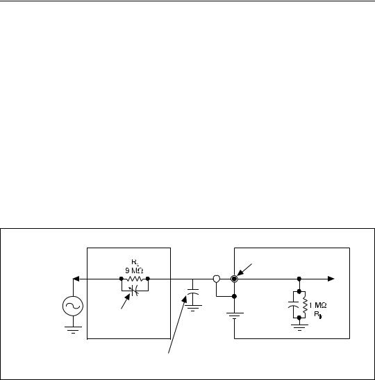
The passive probe is the most widely used general-purpose oscilloscope probe. Passive probes are specified by bandwidth (or rise time), attenuation ratio, compensation range, and mechanical design aspects. Probes with attenuation, X10, X100, or X1000, have a tunable capacitor that can reduce capacitive effects at the input. The ability to cancel or minimize effective capacitance improves the probe’s bandwidth and rise time. Figure 3-6 shows a typical X10 probe model. You should adjust the tunable capacitor, Cp, to obtain a flat frequency response. Cp is the probe capacitance, Rp is the probe resistance, Cin is the input capacitance, Rin is the input resistance.
|
X10 Probe |
Digitizer Input |
|
|
One-tenth of Signal |
|
|
(1 Vpk-to-pk) at Input |
10 Vpk-to-pk |
x pF Cp |
20 pF |
Signal |
Probe Compensation |
Cin |
|
||
|
Adjustment |
|
|
Cc = Lumped Cable |
|
|
Capacitance |
|
|
Figure 3-6. |
Typical X10 Probe |
NI 5102 User Manual |
3-8 |
ni.com |
Chapter 3 Digitizer Basics
Analytically, obtaining a flat frequency response means:
Rin/(Rin + Rp) = Cp/(Cp + Cin + Cc)
It can be shown that:
Rin(Cin + Cc) = CpRp
or the time constant of the probe equals the time constant of the digitizer input.
How to Compensate Your Probe
Adjusting the tunable probe capacitor to get a flat frequency response is called probe compensation. On the NI 5102, you can select a 0–5 V, 1 kHz pulse train as reference to output on PFI1 or PFI2. Calling
niScope_ProbeCompensation in LabVIEW, however, will only allow output to PFI1. Refer to Figure 3-7 as you follow these instructions to compensate your probe:
1.Connect the BNC end of the probe to an input channel, either CH0 or CH1 and select X10 attenuation on the body of the probe tip.
2.Attach the BNC adapter (probe accessory) to the tip of the probe.
3.Connect the SMB100 probe-compensation cable to one of the PFI lines. On the NI 5102 (PXI) this line is PFI1.
4.Attach the probe with the BNC adapter to the BNC female end of the SMB100 cable.
5.Enable the probe compensation signal on the PFI line you selected in step 3. See your application software documentation for more information how to perform this step.
6.Digitize data on the input channel, amplifying the signal until the signal starts to clip. Then go back one step so it does not clip anymore. This step ensures that you use the main dynamic range of the ADC.
7.Adjust the tunable capacitor to make the waveform look as square as possible.
8.For the most accurate measurements, compensate probes for each channel (CH0 and CH1) and use them on that channel only. Recompensate when using the same probe on a different channel.
© National Instruments Corporation |
3-9 |
NI 5102 User Manual |

Chapter 3 Digitizer Basics
CH0 |
|
CH1 |
|
|
BNC Probe |
TRIG |
|
PFI1 |
|
PFI2 |
|
SMB 100 |
BNC Adapter |
NI 5102 (PCI, ISA) |
|
I/O Connectors |
|
Figure 3-7. Connecting the Probe Compensation Cabling
As shown in Figure 3-8, an undercompensated probe attenuates higher frequency signals, whereas an overcompensated probe amplifies higher frequencies. Calibrate your probe frequently to ensure accurate measurements from your NI 5102.
NI 5102 User Manual |
3-10 |
ni.com |