

LM2678
SNVS029J –MARCH 2000–REVISED JULY 2016 |
www.ti.com |
7 Detailed Description
7.1 Overview
The LM2678 provides all of the active functions required for a step-down (buck) switching regulator. The internal power switch is a DMOS power MOSFET to provide power supply designs with high current capability, up to 5 A, and highly efficient operation.
The LM2678 is part of the SIMPLE SWITCHER® family of power converters. The design support WEBENCH, can also be used to provide instant component selection, circuit performance calculations for evaluation, a bill of materials component list and a circuit schematic for LM2678.
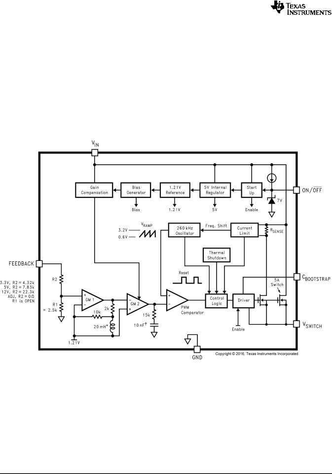
7.2 Functional Block Diagram
7.3 Feature Description
7.3.1 Switch Output
This is the output of a power MOSFET switch connected directly to the input voltage. The switch provides energy to an inductor, an output capacitor and the load circuitry under control of an internal pulse-width-modulator (PWM). The PWM controller is internally clocked by a fixed 260-kHz oscillator. In a standard step-down application the duty cycle (Time ON/Time OFF) of the power switch is proportional to the ratio of the power supply output voltage to the input voltage. The voltage on pin 1 switches between Vin (switch ON) and below ground by the voltage drop of the external Schottky diode (switch OFF).
10 |
Submit Documentation Feedback |
Copyright © 2000–2016, Texas Instruments Incorporated |
Product Folder Links: LM2678