

INMP441
ABSOLUTE MAXIMUM RATINGS
Stress above those listed as Absolute Maximum Ratings may cause permanent damage to the device. These are stress ratings only and functional operation of the device at these conditions is not implied. Exposure to the absolute maximum ratings conditions for extended periods may affect device reliability.
TABLE 4. ABSOLUTE MAXIMUM RATINGS
PARAMETER |
RATING |
Supply Voltage (VDD) |
−0.3 V to +3.63 V |
Digital Pin Input Voltage |
−0.3 V to VDD + 0.3 V or 3.63 V, whichever is less |
Sound Pressure Level |
160 dB |
Mechanical Shock |
10,000 g |
Vibration |
Per MIL-STD-883 Method 2007, Test Condition B |
Temperature Range |
|
Biased |
−40°C to +85°C |
Storage |
−55°C to +150°C |
ESD CAUTION
ESD (electrostatic discharge) sensitive device. Charged devices and circuit boards can discharge without detection. Although this product features patented or proprietary protection circuitry, damage may occur on devices subjected to high energy ESD. Therefore proper ESD precautions should be taken to avoid performance degradation or loss of functionality.
Page 6 of 21
Document Number: DS-INMP441-00
Revision: 1.1
INMP441
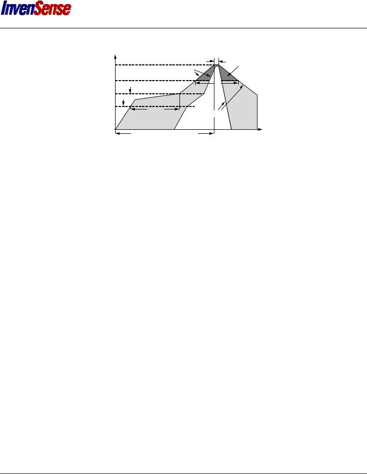
SOLDERING PROFILE
|
|
|
tP |
CRITICAL ZONE |
|
TP |
|
TL TO TP |
|
|
RAMP-UP |
|
|
|
|
|
|
|
|
TEMPERATURE |
TL |
TSMAX |
|
tL |
|
|
|||
|
TSMIN |
|
|
|
|
tS |
|
|
|
|
|
RAMP-DOWN |
||
|
|
PREHEAT |
||
|
|
|
|
|
|
|
t25°C TO PEAK TEMPERATURE |
|
|
|
|
TIME |
|
|
Figure 2. Recommended Soldering Profile Limits
TABLE 5. RECOMMENDED SOLDERING PROFILE*
PROFILE FEATURE |
Sn63/Pb37 |
Pb-Free |
|
Average Ramp Rate (TL to TP) |
1.25°C/sec max |
1.25°C/sec max |
|
|
Minimum Temperature |
100°C |
100°C |
|
(TSMIN) |
|
|
Preheat |
Minimum Temperature |
150°C |
200°C |
|
(TSMIN) |
||
|
|
|
|
|
Time (TSMIN to TSMAX), tS |
60 sec to 75 sec |
60 sec to 75 sec |
Ramp-Up Rate (TSMAX to TL) |
1.25°C/sec |
1.25°C/sec |
|
Time Maintained Above Liquidous (tL) |
45 sec to 75 sec |
~50 sec |
|
Liquidous Temperature (TL) |
183°C |
217°C |
|
Peak Temperature (TP) |
215°C +3°C/−3°C |
260°C +0°C/−5°C |
|
Time Within +5°C of Actual Peak |
20 sec to 30 sec |
20 sec to 30 sec |
|
Temperature (tP) |
|
|
|
Ramp-Down Rate |
3°C/sec max |
3°C/sec max |
|
|
|
|
|
Time +25°C (t25°C) to Peak Temperature |
5 min max |
5 min max |
|
*The reflow profile in Table 5 is recommended for board manufacturing with InvenSense MEMS microphones. All microphones are also compatible with the J-STD-020 profile.
Page 7 of 21
Document Number: DS-INMP441-00
Revision: 1.1