

AT24C01C/AT24C02C
Packaging Information
10.Packaging Information
10.1Package Marking Information
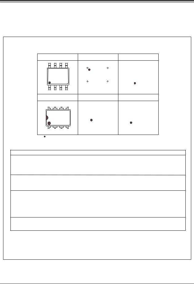
AT24C01C and AT24C02C: Package Marking Information
8-lead SOIC
ATMLHYWW
###% CO YYWWNNN
8-lead PDIP
ATMLUYWW
###% CO YYWWNNN
8-lead TSSOP |
8-pad UDFN |
|
2.0 x 3.0 mm Body |
|
|
|
|
|
|
ATHYWW |
|
|
|
|
|
### |
|
||||
|
|
|
|
|
|
|
|
|
|
|
|
||||||
|
|
|
|
|
|
###%CO |
|
|
|
|
|
H% |
|
||||
|
|
|
|
|
YYWWNNN |
|
|
|
|
|
NNN |
|
|||||
|
|
|
|
|
|
||||||||||||
|
|
|
|
|
|
|
|
|
|
|
|
|
|
|
|
|
|
|
|
|
|
|
|
|
|
|
|
|
|
|
|
||||
5-lead SOT23 |
|
|
|
8-ball VFBGA |
|
||||||||||||
|
|
|
|
|
|
|
|
|
|
|
|
|
|
1.5 x 2.0 mm Body |
|
||
|
|
|
|
|
|
|
|
|
|
|
|
|
|
|
|
|
|
|
|
|
|
|
|
|
|
|
|
|
|
|
|
|
|
|
|
|
|
|
|
|
|
|
|
|
|
|
|
|
|
|
|
|
|
|
|
|
|
|
|
|
|
|
|
|
|
|
|
|
|
###U |
|
|
|
|
|
|
##%UYY |
|
|
|
|
|
|
||||||
|
|
|
|
|
|
WWNNN |
|
|
|
|
|
WNNN |
|
||||
|
|
|
|
|
|
|
|
|
|
|
|
|
|
|
|
|
|
|
|
|
|
|
|
|
|
|
|
|
|
|
|
|
|
|
|
|
|
|
|
|
|
|
|
|
|
|
|
|
|
|
|
|
|
Note 1: |
designates pin 1 |
|
Note 2: Package drawings are not to scale |
|
|
Note 3: For SOT23 package with date codes before 7B, the bottom line (YMXX) is marked on the bottom side and there ryis noofAssemblyCount ( |
@) mark on the top line. |
|
Catalog Number Truncation
AT24C01C |
|
|
|
|
Truncation Code ###: 01C / ##: 1C |
|
|
|
AT24C02C |
|
|
|
|
Truncation Code ###: 02C / ##: 2C |
|
|
|
|
|
|
|
|
|
|
|
|
Date Codes |
|
|
|
|
|
|
Voltages |
|
YY = Year |
|
Y = Year |
|
|
WW = Work Week of Assembly |
|
% = Minimum Voltage |
|
16: 2016 |
20: 2020 |
6: 2016 |
0: 2020 |
02: Week 2 |
|
M: |
1.7V min |
|
17: 2017 |
21: 2021 |
7: 2017 |
1: 2021 |
04: Week 4 |
|
|
|
|
18: 2018 |
22: 2022 |
8: 2018 |
2: 2022 |
... |
|
|
|
|
19: 2019 |
23: 2023 |
9: 2019 |
3: 2023 |
52: Week 52 |
|
|
|
|
|
|
|
|
|
|
|
||
Country of Origin |
|
|
Device Grade |
|
Atmel Truncation |
|||
CO = Country of Origin |
|
|
H or U: |
Industrial Grade |
|
AT: |
Atmel |
|
|
|
|
|
|
|
|
ATM: |
Atmel |
|
|
|
|
|
|
|
ATML: |
Atmel |
|
|
|
|
|
|
|
|
|
Trace Code
NNN = Alphanumeric Trace Code (2 Characters for Small Packages)
© 2018 Microchip Technology Inc. |
Datasheet |
DS20006111A-page 24 |

AT24C01C/AT24C02C
Packaging Information
8-Lead Plastic Dual In-Line (P) - 300 mil Body [PDIP]
Note: For the most current package drawings, please see the Microchip Packaging Specification located at http://www.microchip.com/packaging
D 

 A
A
N |
B |
E1
NOTE 1 
1 2
TOP VIEW
|
E |
C A |
A2 |
PLANE |
|
L |
c |
A1 |
|
e |
eB |
8X b1 
8X b 


 .010
.010
 C
C
SIDE VIEW |
END VIEW |
Microchip Technology Drawing No. C04-018D Sheet 1 of 2
© 2017 Microchip Technology Incorporated
© 2018 Microchip Technology Inc. |
Datasheet |
DS20006111A-page 25 |

AT24C01C/AT24C02C
Packaging Information
8-Lead Plastic Dual In-Line (P) - 300 mil Body [PDIP]
Note: For the most current package drawings, please see the Microchip Packaging Specification located at http://www.microchip.com/packaging
ALTERNATE LEAD DESIGN (VENDOR DEPENDENT)
DATUM A |
|
|
|
|
|
|
|
|
|
|
|
|
|
DATUM A |
|
|
|
|
|
|
|
|
|
|
|
|
|
|
|
|
|
|
|
|
|
|
|
|
|
|
|
|
|
|
|
|
|
|
|
|
|
|
|
|
|
|
|
|
|
|
|
|
|
|
|
|
|
|
|
|
|
|
|
|
|
|
|
|
|
|
|
|
|
|
|
|
|
|
|
|
|
|
|
|
|
|
|
|
|
|
|
|
|
|
|
|
|
|
|
|
|
|
|
|
|
|
|
|
|
|
|
|
|
|
|
|
|
|
|
|
|
|
|
|
|
|
|
|
|
|
|
|
|
|
|
|
|
|
|
|
|
|
|
|
|
|
|
|
|
|
|
|
|
|
|
|
|
|
|
|
|
|
|
|
|
|
|
|
|
|
|
|
|
|
|
|
|
|
|
b |
|
|
|
|
|
|
|
|
|
|
|
|
|
b |
|
|
|
|
|
|
|
|
|
|
|
|
|
|
|
|
|
|
|
|
|
|
|
|
|
|
|
||
|
|
|
|
|
|
|
|
|
|
|
|
|
|
|
|
|
|
|
|
|
|
|
|
|
|
|
||
|
|
|
|
|
|
|
|
|
|
|
|
|
|
|
|
|
|
|
|
|
|
|
|
|
|
|
|
|
e |
|
|
|
|
|
|
|
|
|
|
|
|
|
|
e |
|
|
|
|
|
|
|
|
|
|
|
|
|
2 |
|
|
|
|
|
|
|
|
|
|
|
|
|
|
2 |
|
|
|
|
|
|
|
|
|
|
|
|
|
|
|
|
|
e |
|
|
|
|
|
|
|
|
|
|
|
|
|
e |
|
|
|
|
|
|
|
|
||
|
|
|
|
|
|
|
|
|
|
|
|
|
|
|
|
|
|
|
|
|
|
|
|
|
|
|
|
|
|
|
Units |
|
INCHES |
|
Dimension Limits |
MIN |
NOM |
MAX |
||
Number of Pins |
|
N |
|
8 |
|
Pitch |
|
e |
|
.100 BSC |
|
Top to Seating Plane |
|
A |
- |
- |
.210 |
Molded Package Thickness |
|
A2 |
.115 |
.130 |
.195 |
Base to Seating Plane |
|
A1 |
.015 |
- |
- |
Shoulder to Shoulder Width |
|
E |
.290 |
.310 |
.325 |
Molded Package Width |
|
E1 |
.240 |
.250 |
.280 |
Overall Length |
|
D |
.348 |
.365 |
.400 |
Tip to Seating Plane |
|
L |
.115 |
.130 |
.150 |
Lead Thickness |
|
c |
.008 |
.010 |
.015 |
Upper Lead Width |
|
b1 |
.040 |
.060 |
.070 |
Lower Lead Width |
|
b |
.014 |
.018 |
.022 |
Overall Row Spacing |
§ |
eB |
- |
- |
.430 |
Notes:
1.Pin 1 visual index feature may vary, but must be located within the hatched area.
2.§ Significant Characteristic
3.Dimensions D and E1 do not include mold flash or protrusions. Mold flash or protrusions shall not exceed .010" per side.
4.Dimensioning and tolerancing per ASME Y14.5M
BSC: Basic Dimension. Theoretically exact value shown without tolerances.
Microchip Technology Drawing No. C04-018D Sheet 2 of 2
© 2017 Microchip Technology Incorporated
© 2018 Microchip Technology Inc. |
Datasheet |
DS20006111A-page 26 |

AT24C01C/AT24C02C
Packaging Information
8-Lead Plastic Small Outline (SN) - Narrow, 3.90 mm (.150 In.) Body [SOIC]
Note: For the most current package drawings, please see the Microchip Packaging Specification located at http://www.microchip.com/packaging
|
|
|
2X |
|
|
|
D |
0.10 C |
A–B |
|
|
|
|
|
|
A |
NOTE 5 |
D |
|
|
|
|
||
|
N |
|
|
|
|
|
|
|
|
|
|
|
E |
|
|
E1 |
|
2 |
|
|
2 |
|
|
|
E1 |
|
|
E |
|
NOTE 1 |
1 |
2 |
|
|
e |
NX b |
|
|
B |
0.25 C A–B D |
|
|
|
NOTE 5 |
|
|
TOP VIEW |
|
|
|
|
0.10 |
C |
C A A2 |
|
|
|
SEATING |
|
|
|
PLANE |
|
8X |
|
|
|
0.10 |
C |
A1 |
SIDE VIEW |
|
|

 h
h
|
R0.13 |
|
|
h |
|
H |
R0.13 |
0.23 |
|
||
|
L |
|
|
SEE VIEW C |
|
|
(L1) |
|
|
VIEW A–A |
|
|
VIEW C |
|
|
Microchip Technology Drawing No. C04-057-SN Rev D Sheet 1 of 2 |
|
© 2017 Microchip Technology Incorporated
© 2018 Microchip Technology Inc. |
Datasheet |
DS20006111A-page 27 |

AT24C01C/AT24C02C
Packaging Information
8-Lead Plastic Small Outline (SN) - Narrow, 3.90 mm (.150 In.) Body [SOIC]
Note: For the most current package drawings, please see the Microchip Packaging Specification located at http://www.microchip.com/packaging
|
|
Units |
|
MILLIMETERS |
|
||
|
Dimension Limits |
MIN |
|
NOM |
|
MAX |
|
Number of Pins |
|
N |
|
8 |
|
|
|
Pitch |
|
e |
|
|
1.27 BSC |
|
|
Overall Height |
|
A |
- |
|
- |
|
1.75 |
Molded Package Thickness |
A2 |
1.25 |
|
- |
|
- |
|
Standoff |
§ |
A1 |
0.10 |
|
- |
|
0.25 |
Overall Width |
|
E |
|
|
6.00 BSC |
|
|
Molded Package Width |
E1 |
|
|
3.90 BSC |
|
||
Overall Length |
|
D |
|
|
4.90 BSC |
|
|
Chamfer (Optional) |
|
h |
0.25 |
|
- |
|
0.50 |
Foot Length |
|
L |
0.40 |
|
- |
|
1.27 |
Footprint |
|
L1 |
|
|
1.04 REF |
|
|
Foot Angle |
|
|
0° |
|
- |
|
8° |
Lead Thickness |
|
c |
0.17 |
|
- |
|
0.25 |
Lead Width |
|
b |
0.31 |
|
- |
|
0.51 |
Mold Draft Angle Top |
|
5° |
|
- |
|
15° |
|
Mold Draft Angle Bottom |
|
5° |
|
- |
|
15° |
|
Notes:
1.Pin 1 visual index feature may vary, but must be located within the hatched area.
2.§ Significant Characteristic
3.Dimensions D and E1 do not include mold flash or protrusions. Mold flash or protrusions shall not exceed 0.15mm per side.
4.Dimensioning and tolerancing per ASME Y14.5M
BSC: Basic Dimension. Theoretically exact value shown without tolerances.
REF: Reference Dimension, usually without tolerance, for information purposes only. 5. Datums A & B to be determined at Datum H.
Microchip Technology Drawing No. C04-057-SN Rev D Sheet 2 of 2
© 2017 Microchip Technology Incorporated
© 2018 Microchip Technology Inc. |
Datasheet |
DS20006111A-page 28 |

AT24C01C/AT24C02C
Packaging Information
8-Lead Plastic Small Outline (SN) - Narrow, 3.90 mm Body [SOIC]
Note: For the most current package drawings, please see the Microchip Packaging Specification located at http://www.microchip.com/packaging
SILK SCREEN
C
Y1
X1
E 

RECOMMENDED LAND PATTERN
|
|
Units |
|
MILLIMETERS |
|
||
|
Dimension Limits |
MIN |
|
NOM |
|
MAX |
|
Contact Pitch |
|
E |
|
|
1.27 BSC |
|
|
Contact Pad Spacing |
|
C |
|
|
5.40 |
|
|
Contact Pad Width (X8) |
|
X1 |
|
|
|
|
0.60 |
Contact Pad Length (X8) |
|
Y1 |
|
|
|
|
1.55 |
Notes:
1. Dimensioning and tolerancing per ASME Y14.5M
BSC: Basic Dimension. Theoretically exact value shown without tolerances.
Microchip Technology Drawing C04-2057-SN Rev B
© 2017 Microchip Technology Incorporated
© 2018 Microchip Technology Inc. |
Datasheet |
DS20006111A-page 29 |

AT24C01C/AT24C02C
Packaging Information
!
" # 1 % & % ! % 2 " ) ' % 2$% % " %
%% 033))) & &3 2
|
D |
N |
|
|
E |
|
E1 |
NOTE 1 |
|
1 |
2 |
b |
|
|
e |
|
|
|
|
|
|
|
|
|
|
|
|
|
|
|
|
|
|
|
c |
|
|
|
|
|
|
|
|
|
|
|
|
φ |
||||
|
|
|
|
|
|
|
|
|
|
|
|
|
|
|
|
|
|
|
|
|
|
|
|
|
|
|
|
|
|
|
||||||
A |
|
|
|
|
|
|
|
|
|
|
|
A2 |
|
|
|
|
|
|
|
|
|
|
|
|
|
|
|
|||||||||
|
|
|
|
|
|
|
|
|
|
|
|
|
|
|
|
|
|
|
|
|
|
|
|
|
|
|
|
|
|
|
|
|
|
|
|
|
|
|
A1 |
|
|
|
|
|
|
|
|
|
|
|
|
|
|
|
|
|
|
|
L1 |
|
|
|
|
L |
|
|
|
|
|
|
|
|
|
|
|
|
|
|
|
|
|
|
|
|
|
|
|
|
|
|
|
|
|
|
|
|
|
|
|
|
|
|
|
|
|
|
||||
|
|
|
|
|
|
|
|
|
|
|
|
|
|
|
|
|
|
|
|
|
|
|
|
|
|
|
|
|
||||||||
|
|
|
|
|
|
|
|
|
|
|
|
|
|
|
|
|
|
|
|
|
|
|
|
|
|
|
|
|
|
|
|
|
||||
|
|
|
|
|
|
|
|
|
|
|
|
|
|
|
|
|
|
|
|
|
|
|
|
|
|
|
|
|
|
|
|
|
|
|
|
|
|
|
|
|
|
|
|
|
|
|
|
|
|
|
|
|
|
|
|
4 % |
|
|
|
|
|
55 * * |
|
|
|
|
|
||||||
|
|
|
|
|
|
|
|
|
|
|
|
|
|
|
|
|
& 5 & % |
|
6 |
|
67 |
|
|
|
8 |
|||||||||||
6!&($ |
6 |
|
|
|
|
|
|
9 |
|
|
|
|
|
|
|
|
||||||||||||||||||||
% |
|
|
|
|
|
|
|
|
|
|
:+ . / |
|
|
|
|
|
||||||||||||||||||||
7 ; % |
|
|
|
|
< |
|
|
< |
|
|
|
|
||||||||||||||||||||||||
" " 2 2 |
|
|
|
|
9 |
|
|
|
|
|
+ |
|||||||||||||||||||||||||
% "$$ |
|
|
|
|
+ |
|
< |
|
|
|
+ |
|||||||||||||||||||||||||
7 = "% |
* |
|
|
|
|
|
|
|
: . / |
|
|
|
|
|
||||||||||||||||||||||
" " 2 = "% |
|
|
* |
|
, |
|
|
|
|
|
+ |
|||||||||||||||||||||||||
" " 2 5 % |
|
|
|
|
|
|
, |
|
|
|
, |
|||||||||||||||||||||||||
1 % 5 % |
5 |
|
|
+ |
|
: |
|
|
|
+ |
||||||||||||||||||||||||||
1 % % |
|
|
5 |
|
|
|
|
|
|
*1 |
|
|
|
|
|
|||||||||||||||||||||
1 % |
|
|
|
|
> |
< |
|
|
|
9> |
|
|
|
|||||||||||||||||||||||
5 " 2 |
|
|
|
|
|
|
< |
|
|
|
|
|||||||||||||||||||||||||
5 " = "% |
( |
|
|
|
< |
|
|
|
, |
|||||||||||||||||||||||||||
" #
! " #$%! & ' (!% &! % ( % " ) % % % "
& " * " % !" & "$ % ! "$ % ! % # " + && " , & " % *-+
. /0 . & % # % ! ) ) % !% %
*10 $& ' ! ! ) % !% % '$ $& % !
) / 9:.
© 2017 Microchip Technology Incorporated
© 2018 Microchip Technology Inc. |
Datasheet |
DS20006111A-page 30 |
AT24C01C/AT24C02C
Packaging Information
Note: For the most current package drawings, please see the Microchip Packaging Specification located at http://www.microchip.com/packaging
© 2017 Microchip Technology Incorporated
© 2018 Microchip Technology Inc. |
Datasheet |
DS20006111A-page 31 |

AT24C01C/AT24C02C
Packaging Information
5-Lead Plastic Thin Small Outline Transistor (NMB) [TSOT]
Atmel Legacy Global Package Code TSZ
Note: For the most current package drawings, please see the Microchip Packaging Specification located at http://www.microchip.com/packaging
D |
0.20 |
C |
2X |
|
|
|
|
e1 |
|
|
|
A |
|
|
D |
|
|
|
|
N |
|
|
|
|
|
E/2 |
|
E1/2 |
|
|
|
E1 |
|
|
E |
|
(DATUM D) |
|
|
|
(DATUM A-B) |
||
0.15 C D |
|
|
2X |
|
|
NOTE 1 |
1 |
2 |
|
|
0.20 C |
|
e |
|
|
B |
NX b |
|
|
0.20 C A-B D |
TOP VIEW
 A
A

 A
A
SEE SHEET 2
A |
A2 |
0.20 |
C |
|
|
||
|
|
SEATING PLANE |
|
|
A1 |
C |
|
SIDE VIEW
Microchip Technology Drawing C04-21344 Rev B Sheet 1 of 2
© 2018 Microchip Technology Inc. |
Datasheet |
DS20006111A-page 32 |

AT24C01C/AT24C02C
Packaging Information
5-Lead Plastic Thin Small Outline Transistor (NMB) [TSOT]
Atmel Legacy Global Package Code TSZ
Note: For the most current package drawings, please see the Microchip Packaging Specification located at http://www.microchip.com/packaging
(c)
θ 
L
L1
VIEW A-A
SHEET 1
|
Units |
|
MILLIMETERS |
|
||
Dimension Limits |
MIN |
|
NOM |
|
MAX |
|
Number of Leads |
N |
|
5 |
|
|
|
Pitch |
e |
|
|
0.95 BSC |
|
|
Outside lead pitch |
e1 |
|
|
1.90 BSC |
|
|
Overall Height |
A |
- |
|
- |
|
1.10 |
Molded Package Thickness |
A2 |
0.70 |
|
0.90 |
|
1.00 |
Standoff |
A1 |
- |
|
- |
|
0.10 |
Overall Width |
E |
|
|
2.80 BSC |
|
|
Molded Package Width |
E1 |
|
|
1.60 BSC |
|
|
Overall Length |
D |
|
|
2.90 BSC |
|
|
Foot Length |
L |
0.30 |
|
- |
|
0.60 |
Footprint |
L1 |
|
|
0.60 REF |
|
|
Foot Angle |
θ |
0° |
- |
|
8° |
|
Lead Thickness |
c |
0.08 |
- |
|
0.20 |
|
Lead Width |
b |
0.30 |
- |
|
0.50 |
|
Notes:
1.Dimensions D and E1 do not include mold flash or protrusions. Mold flash or protrusions shall not exceed 0.25mm per side.
2.Dimensioning and tolerancing per ASME Y14.5M
BSC: Basic Dimension. Theoretically exact value shown without tolerances.
REF: Reference Dimension, usually without tolerance, for information purposes only.
Microchip Technology Drawing C04-21344 Rev B Sheet 2 of 2
© 2018 Microchip Technology Inc. |
Datasheet |
DS20006111A-page 33 |

AT24C01C/AT24C02C
Packaging Information
5-Lead Plastic Thin Small Outline Transistor (NMB) [TSOT]
Atmel Legacy Global Package Code TSZ
Note: For the most current package drawings, please see the Microchip Packaging Specification located at http://www.microchip.com/packaging
X1 
5
Y1
SILK SCREEN
C
1 |
|
|
|
E |
|
|
|
|
2 |
|
|
|
|
|
G |
|
|
|
|
|
|||||||||||||
|
|
|
|
|
|
|
|
|
|
|
|
|
|
|
||
|
|
|
|
|
|
|
|
|
|
|
|
|
|
|
||
|
|
|
|
|
|
|
|
|
|
|
|
|
|
|
||
|
|
|
|
|
|
|
|
|||||||||
|
|
|
|
|
|
|
|
|
|
|
|
|
|
|||
|
|
|
|
|
|
|
|
|
|
|
|
|
|
|
|
|
|
|
|
|
|
|
|
|
|
|
|
|
|
||||
RECOMMENDED LAND PATTERN
|
Units |
|
MILLIMETERS |
|
||
Dimension Limits |
MIN |
|
NOM |
|
MAX |
|
Contact Pitch |
E |
|
|
0.95 BSC |
|
|
Contact Pad Spacing |
C |
|
|
2.60 |
|
|
Contact Pad Width (X5) |
X1 |
|
|
|
|
0.60 |
Contact Pad Length (X5) |
Y1 |
|
|
|
|
1.05 |
Contact Pad to Center Pad (X2) |
G |
0.20 |
|
|
|
|
Notes:
1. Dimensioning and tolerancing per ASME Y14.5M
BSC: Basic Dimension. Theoretically exact value shown without tolerances.
2.For best soldering results, thermal vias, if used, should be filled or tented to avoid solder loss during reflow process
Microchip Technology Drawing C04-23344 Rev B
© 2018 Microchip Technology Inc. |
Datasheet |
DS20006111A-page 34 |

AT24C01C/AT24C02C
Packaging Information
8-Lead Ultra Thin Plastic Dual Flat, No Lead Package (Q4B) - 2x3 mm Body [UDFN] Atmel Legacy YNZ Package
Note: For the most current package drawings, please see the Microchip Packaging Specification located at http://www.microchip.com/packaging
|
|
|
|
|
D |
A |
B |
|
|
|
|
|
|
|
|
|
|
|
|
|
|
|
|
|
|
|
|
|
|
|
|
N |
|
|
|
|
|
|
|
|
|
(DATUM A) |
|
|
|
|
|
|
|
|
|
|
|
|
|
(DATUM B) |
|
|
|
|
|
E |
|
|
|
|
|
|
|
|
|
|
|
|
|
|
|
|
|
|
|
||
|
NOTE 1 |
|
|
|
|
|
|
|
|
|
|
|
|
|
2X |
|
|
|
|
|
|
|
|
|
|
|
|
|
0.10 |
C |
|
|
|
|
|
|
|
|
|
|
|
|
2X |
|
|
1 |
2 |
|
|
|
|
|
|
|
|
|
|
|
TOP VIEW |
|
|
|
|
|
|
|
|
||
|
|
0.10 |
C |
|
|
|
|
|
|
|
|
||
C |
|
|
|
|
|
|
0.10 |
C |
|
|
A1 |
|
|
A |
|
|
|
|
|
|
|
|
|
|
|
|
|
SEATING |
|
|
|
|
|
|
|
|
|
|
|
|
|
PLANE |
(A3) |
|
|
|
|
8X |
|
|
|
|
|
|
|
|
|
|
|
|
0.08 |
C |
|
|
|
|
|
||
|
|
|
SIDE VIEW |
|
|
|
|
|
|
||||
|
|
|
|
|
|
|
|
|
|
||||
|
|
|
|
|
|
|
|
|
|
|
|
||
|
0.10 |
C |
A |
B |
D2 |
|
|
|
|
|
|
|
|
|
|
|
|
|
|
|
|
|
|
|
|
|
|
|
|
|
|
|
e |
|
|
|
|
|
|
|
|
|
|
|
|
|
2 |
|
|
|
|
|
|
|
|
|
|
|
|
1 |
2 |
|
|
|
|
|
|
|
|
|
|
|
|
|
|
|
|
|
0.10 |
|
C |
A |
B |
|
|
|
|
|
|
|
E2 |
|
K |
|
|
|
|
|
|
|
|
|
|
|
|
|
|
|
|
|
|
|
L |
|
|
N |
|
|
|
|
|
|
|
|
|
|
|
|
|
|
8X b |
|
|
|
|
|
|
||
|
|
|
|
|
|
|
|
|
|
|
|
||
|
|
|
|
e |
|
|
0.10 |
C |
A |
B |
|
|
|
|
|
|
BOTTOM VIEW |
|
0.05 |
C |
|
|
|
|
|||
|
|
|
|
|
|
|
|
|
|
|
|||
Microchip Technology Drawing C04-21355-Q4B Rev A Sheet 1 of 2
© 2017 Microchip Technology Inc.
© 2018 Microchip Technology Inc. |
Datasheet |
DS20006111A-page 35 |

AT24C01C/AT24C02C
Packaging Information
8-Lead Ultra Thin Plastic Dual Flat, No Lead Package (Q4B) - 2x3 mm Body [UDFN] Atmel Legacy YNZ Package
Note: For the most current package drawings, please see the Microchip Packaging Specification located at http://www.microchip.com/packaging
|
Units |
|
MILLIMETERS |
|
||
Dimension Limits |
MIN |
|
NOM |
|
MAX |
|
Number of Terminals |
N |
|
8 |
|
|
|
Pitch |
e |
|
|
0.50 BSC |
|
|
Overall Height |
A |
0.50 |
|
0.55 |
|
0.60 |
Standoff |
A1 |
0.00 |
|
0.02 |
|
0.05 |
Terminal Thickness |
A3 |
|
|
0.152 REF |
|
|
Overall Length |
D |
|
|
2.00 BSC |
|
|
Exposed Pad Length |
D2 |
1.40 |
|
1.50 |
|
1.60 |
Overall Width |
E |
|
|
3.00 BSC |
|
|
Exposed Pad Width |
E2 |
1.20 |
1.30 |
|
1.40 |
|
Terminal Width |
b |
0.18 |
0.25 |
|
0.30 |
|
Terminal Length |
L |
0.35 |
0.40 |
|
0.45 |
|
Terminal-to-Exposed-Pad |
K |
0.20 |
- |
|
- |
|
Notes:
1.Pin 1 visual index feature may vary, but must be located within the hatched area.
2.Package is saw singulated
3.Dimensioning and tolerancing per ASME Y14.5M
BSC: Basic Dimension. Theoretically exact value shown without tolerances.
REF: Reference Dimension, usually without tolerance, for information purposes only.
Microchip Technology Drawing C04-21355-Q4B Rev A Sheet 2 of 2
© 2017 Microchip Technology Inc.
© 2018 Microchip Technology Inc. |
Datasheet |
DS20006111A-page 36 |

AT24C01C/AT24C02C
Packaging Information
8-Lead Ultra Thin Plastic Dual Flat, No Lead Package (Q4B) - 2x3 mm Body [UDFN] Atmel Legacy YNZ Package
Note: For the most current package drawings, please see the Microchip Packaging Specification located at http://www.microchip.com/packaging
|
X2 |
|
EV |
|
G2 |
|
8 |
|
ØV |
C |
Y2 |
|
G1 |
Y1
1 |
|
2 |
|
|
|
|
|
|
|
|
|
|
|
|
|
|
|||||
SILK SCREEN |
|
|
|
|
|
|
|
|
|
X1 |
|
|
|
|
|
|
|
|
|
|


 E
E 

RECOMMENDED LAND PATTERN
|
Units |
|
MILLIMETERS |
|
||
Dimension Limits |
MIN |
|
NOM |
|
MAX |
|
Contact Pitch |
E |
|
|
0.50 BSC |
|
|
Optional Center Pad Width |
X2 |
|
|
|
|
1.60 |
Optional Center Pad Length |
Y2 |
|
|
|
|
1.40 |
Contact Pad Spacing |
C |
|
|
2.90 |
|
|
Contact Pad Width (X8) |
X1 |
|
|
|
|
0.30 |
Contact Pad Length (X8) |
Y1 |
|
|
|
|
0.85 |
Contact Pad to Center Pad (X8) |
G1 |
0.20 |
|
|
|
|
Contact Pad to Contact Pad (X6) |
G2 |
0.33 |
|
|
|
|
Thermal Via Diameter |
V |
|
|
0.30 |
|
|
Thermal Via Pitch |
EV |
|
|
1.00 |
|
|
Notes:
1. Dimensioning and tolerancing per ASME Y14.5M
BSC: Basic Dimension. Theoretically exact value shown without tolerances.
2.For best soldering results, thermal vias, if used, should be filled or tented to avoid solder loss during reflow process
Microchip Technology Drawing C04-21355-Q4B Rev A
© 2017 Microchip Technology Inc.
© 2018 Microchip Technology Inc. |
Datasheet |
DS20006111A-page 37 |

AT24C01C/AT24C02C
Packaging Information
|
|
|
|
|
|
|
|
|
|
|
|
|
|
|
|
|
|
|
|
|
|
|
|
d |
|
0.10 |
(4X) |
|
|
|
|
|
|
|
|
|
|
|
|
|
|
|
|
|
|
|
|
|
|
|
|
|
|
|
|
|
|
|
|
|
||||||
|
|
|
|
|
|
|
|
|
|
|
|
|
|
|
|
|
|
|
|
|
|
|
|
|
|
|
|
|
|
|
|
|
|
|
|
|
|
|
|
|
|
|
|
|
|
|
|
|
|
|
|
d |
|
|
0.08 |
C |
|
|
|
|
|
|||||
|
|
|
|
|
|
|
|
E |
|
|
|
|
|
|
|
|
|
|
|
|
|
|
|
|
|
|
|
|
|
|
|
|
|
|
|
f |
0.10 |
C |
|
|
|
|
|
|
|
|
|
|
|
|
|
|
|
|
|
|
|
|
|
|
|
|
|
|||
|
|
|
|
|
|
|
|
|
|
|
|
|
|
|
|
|
|
|
|
|
|
|
|
|
|
A |
|
|
|
|
|
|
|
|
|
|
|
|
|
|
|
|
|
|
|
|
|
C |
|
|
|
|
|
|
|
|
|
|
|
|
||||||
|
|
|
|
|
|
|
|
|
|
|
|
|
|
|
|
|
|
|
|
|
|
|
|
|
|
|
|
|
|
|
|
|
|
|
|
|
|
|
|
|
|
|
|
|
|
|
|
|
|
|
|
|
|
|
|
|
|
|
|
|
|
|
||||
|
|
|
|
|
|
|
|
|
|
|
|
|
|
|
|
|
|
|
|
|
|
|
|
|
|
|
|
|
|
|
|
|
|
|
|
|
|
|
|
|
|
|
|
|
|
|
|
|
|
|
|
|
|
|
|
|
|
|
|
|
|
|
|
|
|
|
|
|
|
|
|
|
|
|
|
|
|
|
|
|
|
|
|
|
|
|
|
|
|
|
|
|
|
|
|
|
|
|
|
|
|
|
|
|
|
|
|
|
|
|
|
|
|
|
|
|
|
|
|
|
|
|
|
|
|
|
|
|
|
|
|
|
|
|
|
|
|
|
|
|
|
|
|
|
|
|
|
|
|
|
|
|
|
|
|
|
|
|
|
|
|
|
|
|
|
|
|
|
|
|
|
|
|
|
|
|
|
|
|
|
|
|
|
|
|
|
|
|
|
|
|
|
|
|
|
|
|
|
|
|
|
|
|
|
|
|
|
|
|
|
|
|
|
|
|
|
|
|
|
|
|
|
|
|
|
|
|
|
|
|
|
|
|
|
|
|
|
|
|
|
|
|
|
|
|
|
|
|
|
|
|
|
|
|
|
|
|
|
|
|
|
|
|
|
|
|
|
|
|
|
|
|
|
|
|
|
|
|
|
|
|
|
|
|
|
|
|
|
|
|
|
|
|
|
|
|
|
|
|
|
|
|
|
|
|
|
|
|
|
|
|
|
|
|
|
|
|
|
|
|
|
|
|
|
|
|
|
|
|
|
|
|
|
|
|
|
|
|
|
|
|
|
|
|
|
|
|
|
|
|
|
|
|
|
|
|
|
|
|
|
|
|
D |
|
|
|
|
|
|
|
|
|
|
|
|
|
|
|
|
|
|
|
|
|
|
|
|
2. |
b |
|
|
|
|
||||||||
|
|
|
|
|
|
|
|
|
|
|
|
|
|
|
|
|
|
|
|
|
|
|
|
|
|
|
|
|
|
|
|
|
|
|
|
|
|
|
|
|
|
|
|
|
|
|
|
|
|
|
|
|
|
|
||||||||||||
|
|
|
|
|
|
|
|
|
|
|
|
|
|
|
|
|
|
|
|
|
|
|
|
|
|
|
|
|
|
|
|
|
|
|
|
|
|
|
|
|
|
|
|
|
|
|
|
|
|
|
|
|
|
|
|
|
|
|
|
|
||||||
|
|
|
|
|
|
|
|
|
|
|
|
|
|
|
|
|
|
|
|
|
|
|
|
|
|
|
|
|
|
|
|
|
|
|
|
|
|
|
|
|
|
|
|
|
|
|
|
|
|
|
|
|
|
|
|
|
|
|
j |
n 0.15 m |
C |
A |
B |
|||
|
|
|
|
|
|
|
|
|
|
|
|
|
|
|
|
|
|
|
|
|
|
|
|
|
|
|
|
|
|
|
|
|
|
|
|
|
|
|
|
|
|
|
|
|
|
|
|
|
|
|
|
|
|
|
|
|
|
|
j |
n 0.08m |
C |
|
|
|||
|
|
|
|
|
|
|
|
|
|
|
|
|
|
|
|
|
|
|
|
|
|
|
|
|
|
|
|
|
|
|
|
|
|
|
|
|
|
|
|
|
|
|
|
|
|
|
|
|
|
|
|
|
|
|
|
|
|
|
|
|
|
|
|
|
|
|
|
|
|
|
|
|
|
|
|
|
|
|
|
|
|
|
|
|
|
|
|
|
|
|
|
|
|
|
|
|
|
|
|
|
|
|
|
|
|
|
|
|
|
|
|
|
|
|
|
|
|
|
|
|
|
|
|
|
|
|
|
|
|
|
|
|
|
|
|
|
|
|
|
|
|
|
|
|
|
|
|
|
|
|
|
|
|
|
|
|
|
|
|
|
|
|
|
|
|
|
|
|
|
|
|
|
|
|
|
|
|
|
|
|
|
|
|
|
|
|
|
|
|
|
|
|
|
|
|
|
|
|
|
|
|
|
|
|
|
|
|
PIN 1 BALL PAD CORNER |
|
B |
A2 |
|
|
|
|
|
|
|
|
|
|
|
|
|
|
|
|
|
|
|
A1 |
|
|
|
|
|
|
|
|||||||||||||||||||||||||||||
|
|
|
|
|
|
|
TOP VIEW |
|
|
|
|
|
|
|
|
|
|
|
|
|
|
|
|
|
|
|
|
|
|
|
|
|
|
|
|
|
|
|
|
|
|
|
|
|
|
|
|
|
|
|
|
|
|
|||||||||||||
|
|
|
|
|
|
|
|
|
|
|
|
|
|
|
|
|
|
|
|
|
|
|
|
|
|
|
|
|
|
|
|
|
|
|
|
|
|
|
|
|
|
|
|
|
|
|
|
|
|
|
|
|
||||||||||||||
|
|
|
|
|
|
|
|
|
|
|
|
|
|
|
|
|
|
|
|
|
|
|
|
|
|
|
|
|
A |
|
|
|
|
|
|
|
|
|
|
|
|
|
|
|
|
|
|
|
|
|
|
|
|
|||||||||||||
|
|
|
|
|
|
|
|
|
|
|
|
|
|
|
|
|
|
|
|
|
|
|
|
|
|
|
|
|
|
|
|
|
|
|
|
|
|
|
|
|
|
|
|
|
|
|
|
|
|
|
||||||||||||||||
|
|
PIN 1 BALL PAD CORNER |
|
|
|
|
|
|
|
|
|
|
|
|
|
|
|
|
|
SIDE VIEW |
|
|
|
|
|
|
|
|
|
|
|
|
||||||||||||||||||||||||||||||||||
|
|
4 |
|
|
|
|
|
|
|
|
|
|
|
|
|
|
|
|
|
|
|
|
|
|
|
|
|
|
|
|
|
|
|
|
|
|
|
|
|
|
|
|
|
|
|
|
|
|
||||||||||||||||||
1 |
2 |
3 |
|
|
|
|
|
|
|
|
|
|
|
|
|
|
|
|
|
|
|
|
|
|
|
|
|
|
|
|
|
|
|
|
|
|
|
|
|
|
|
|
|
|
|
|
|
|
|
|
|
|
|
|
||||||||||||
|
|
|
|
|
|
|
|
|
|
|
|
|
|
|
|
|
|
|
|
|
|
|
|
|
|
|
|
|
|
|
|
|
|
|
|
|
|
|
|
|
|
|
|
|
|
|
|
|
|
|
|
|
|
|
|
|
|
|
|
|
|
|
|
|
||
|
|
|
|
|
|
|
|
|
|
|
|
|
|
|
|
|
|
|
|
|
|
|
|
|
|
|
|
|
|
|
|
|
|
|
|
|
|
|
|
|
|
|
|
|
|
|
|
|
|
|
|
|
|
|
|
|
|
|
|
|
|
|
|
|
|
|
|
|
|
|
|
|
|
|
|
|
|
|
|
|
|
|
|
|
|
|
|
|
|
|
|
|
|
|
|
|
|
|
|
|
|
|
|
|
|
|
|
|
|
|
|
|
|
|
|
|
|
|
|
|
|
|
|
|
|
|
|
|
|
|
|
|
|
|
|
|
|
|
|
|
|
|
|
|
|
|
|
|
|
|
|
|
|
|
|
|
|
|
|
|
|
|
|
|
|
|
|
|
|
|
|
|
|
|
|
|
|
|
|
|
|
|
|
|
|
|
|
|
|
|
|
|
|
|
|
|
|
|
||
|
|
|
|
|
|
|
|
|
|
|
|
|
|
|
|
|
|
|
|
|
|
|
|
|
|
|
|
d |
|
|
|
|
|
|
|
|
|
|
|
|
|
|
|
|
|
|
|
|
|
|
|
|
|
|
|
|
|
|
|
|
|
|||||
|
|
|
|
|
|
|
|
|
|
|
|
|
|
|
|
|
|
|
|
|
|
|
|
|
|
|
|
|
|
|
|
|
|
|
|
|
|
|
|
|
|
|
|
|
|
|
|
|
|
|
|
|
|
|
|
|
|
|
|
|
|
|
|
|
|
|
|
|
|
|
|
|
|
|
|
|
|
|
|
|
|
|
|
|
|
|
|
|
|
|
|
|
|
|
|
|
|
|
|
|
|
|
|
|
|
|
|
|
|
|
|
|
|
|
|
|
|
|
|
|
|
|
|
|
|
|
|
|
|
|
|
|
|
|
|
|
|
|
|
|
|
|
|
|
|
|
|
|
|
|
|
|
|
|
|
|
|
|
|
|
|
|
|
|
|
|
|
|
|
|
|
|
|
|
|
|
|
|
|
|
|
|
|
|
|
|
|
|
|
|
|
|
|
|
|
|
|
|
|
|
|
|
|
|
|
|
|
|
|
|
|
|
|
|
|
|
|
|
|
|
|
|
|
|
|
|
|
(d1) |
|
|
|
|
|
|
|
|
|
|
|
|
|
|
|
|
|
|
|
|
|
|
|
|
|
|
|
|
|
|
|
|
|
||||||
|
|
|
|
|
|
|
|
|
|
|
|
|
|
|
|
|
|
|
|
|
|
|
|
|
|
|
|
|
|
|
|
|
|
|
|
|
|
|
|
|
|
|
|
|
|
|
|
|
|
|
|
|
|
|
|
|
|
|
|
|||||||
|
|
|
|
|
|
|
|
|
|
|
|
|
|
|
|
|
|
|
|
|
|
|
|
|
|
|
|
|
|
|
|
|
|
|
|
|
|
|
|
|
|
|
|
|
|
|
|
|
|
|
|
|
|
|
|
|
|
|
|
|
|
|||||
|
|
|
8 |
7 |
|
|
6 |
|
e |
|
|
|
5 |
|
|
|
|
|
|
|
|
|
|
|
|
|
|
|
COMMON DIMENSIONS |
|
|
|
|
|||||||||||||||||||||||||||||||||
|
|
|
|
|
|
|
|
|
|
|
|
|
|
|
|
|
|
|
|
|
|
|||||||||||||||||||||||||||||||||||||||||||||
|
|
|
|
|
|
|
|
|
|
|
|
|
|
|
|
|
|
|
|
|
|
|
|
|
|
|
|
|
|
|
|
|
|
|
|
|
|
|
|
|||||||||||||||||||||||||||
|
|
|
|
|
|
|
|
|
|
|
|
|
|
|
|
|
|
|
|
|
|
|
|
|
|
|
|
|
|
|
|
|
|
|
|
|
||||||||||||||||||||||||||||||
|
|
|
|
|
|
|
|
|
|
|
|
(e1) |
|
|
|
|
|
|
|
|
|
|
|
|
|
|
|
|
|
|
|
|
|
|
(Unit of Measure - mm) |
|
|
|
|
|
|
|
||||||||||||||||||||||||
|
|
|
|
|
|
|
|
|
|
|
|
|
|
|
|
|
|
|
|
|
|
|
|
|
|
|
|
|
|
|
|
|
|
|
|
|
|
|
|
|
|
|
|
|
|
|
|
|
|
|
|
|
|
|
|
|
|
|
|
|
|
|
||||
|
|
|
|
|
|
BOTTOM VIEW |
|
|
|
|
|
|
|
|
|
|
|
|
|
|
|
|
SYMBOL |
MIN |
|
NOM |
|
|
|
MAX |
|
|
NOTE |
|
|
|||||||||||||||||||||||||||||||
|
|
|
|
|
|
|
|
|
|
|
|
|
|
|
|
|
|
|
|
|
|
|
A |
0.73 |
|
|
0.79 |
|
|
|
|
|
0.85 |
|
|
|
|
|
|
|
||||||||||||||||||||||||||
|
|
|
|
|
|
|
8 SOLDER BALLS |
|
|
|
|
|
|
|
|
|
|
|
|
|
|
|
|
|
A1 |
0.09 |
|
|
0.14 |
|
|
|
|
|
0.19 |
|
|
|
|
|
|
|
||||||||||||||||||||||||
Notes: |
|
|
|
|
|
|
|
|
|
|
|
|
|
|
|
|
|
|
|
|
|
|
|
|
|
|
|
|
|
|
A2 |
0.40 |
|
|
0.45 |
|
|
|
|
|
0.50 |
|
|
|
|
|
|
|
||||||||||||||||||
|
|
|
|
|
|
|
|
|
|
|
|
|
|
|
|
|
|
|
|
|
|
|
|
|
|
|
|
|
|
b |
0.20 |
|
|
0.25 |
|
|
|
|
|
0.30 |
|
2 |
|
|
|
|
||||||||||||||||||||
|
|
|
|
|
|
|
|
|
|
|
|
|
|
|
|
|
|
|
|
|
|
|
|
|
|
|
|
|
|
|
|
|
|
|
|
|
|
|
|
|
|
|
|
|
|
|
|
|||||||||||||||||||
1. This drawing is for general information only. |
|
|
|
|
|
|
|
|
|
|
|
|
|
|
|
|
|
D |
|
|
|
|
|
|
|
1.50 BSC |
|
|
|
|
|
|
|
|
|
|
|
|
||||||||||||||||||||||||||||
2. Dimension ‘b’ is measured at maximum solder ball diameter. |
|
|
E |
|
|
|
|
|
|
|
2.0 BSC |
|
|
|
|
|
|
|
|
|
|
|
|
|||||||||||||||||||||||||||||||||||||||||||
|
|
e |
|
|
|
|
|
|
|
0.50 BSC |
|
|
|
|
|
|
|
|
|
|
|
|
||||||||||||||||||||||||||||||||||||||||||||
|
|
|
|
|
|
|
|
|
|
|
|
|
|
|
|
|
|
|
|
|
|
|
|
|
|
|
|
|
|
|
|
|
|
|
|
|
|
|
|
|
|
|
|
|
|
|
|
|
|
|
|
|
|
|
||||||||||||
3. Solder ball composition shall be 95.5Sn-4.0Ag-.5Cu. |
|
|
e1 |
|
|
|
|
|
|
|
0.25 REF |
|
|
|
|
|
|
|
|
|
|
|
|
|||||||||||||||||||||||||||||||||||||||||||
|
|
|
|
|
|
|
|
|
|
|
|
|
|
|
|
|
|
|
|
|
|
|
||||||||||||||||||||||||||||||||||||||||||||
|
|
d |
|
|
|
|
|
|
|
1.00 BSC |
|
|
|
|
|
|
|
|
|
|
|
|
||||||||||||||||||||||||||||||||||||||||||||
|
|
|
|
|
|
|
|
|
|
|
|
|
|
|
|
|
|
|
|
|
|
|
|
|
|
|
|
|
|
|
|
|
|
|
|
|
|
|
|
|
|
|
|
|
|
|
|
|
|
|
|
|
|
|
||||||||||||
|
|
|
|
|
|
|
|
|
|
|
|
|
|
|
|
|
|
|
|
|
|
|
|
|
|
|
|
|
|
|
|
|
|
|
|
|
|
|
|
|
|
|
|
|
|
|
|
|
|
|
|
|
|
|
|
|
|
|
|
|
|
|
|
|
|
|
|
|
|
|
|
|
|
|
|
|
|
|
|
|
|
|
|
|
|
|
|
|
|
|
|
|
|
|
|
|
|
|
|
|
|
|
d1 |
|
|
|
|
|
|
|
0.25 REF |
|
|
|
|
|
|
|
|
|
|
|
|
||||||||||
|
|
|
|
|
|
|
|
|
|
|
|
|
|
|
|
|
|
|
|
|
|
|
|
|
|
|
|
|
|
|
|
|
|
|
|
|
|
|
|
|
|
|
|
|
|
|
|
|
|
|
|
|
|
|
|
|
|
|
|
|
|
|
|
|
|
|
|
|
|
|
7/1/14 |
|
|
|
|
|
|
TITLE |
GPC |
DRAWING NO . |
REV. |
|
8U3-1, 8-ball, 1.50mm x 2.00mm body, 0.50mm pitch, |
GXU |
8U3-1 |
G |
|
Very Thin, Fine-Pitch Ball Grid Array Package (VFBGA) |
|||
|
|
|
|
|
|
|
|
|
|
Note: For the most current package drawings, please see the Microchip Packaging Specification located at http://www.microchip.com/packaging.
© 2018 Microchip Technology Inc. |
Datasheet |
DS20006111A-page 38 |