

AT24C01C/AT24C02C
I²C-Compatible (Two-Wire) Serial EEPROM 1 Kbit (128 x 8), 2 Kbit (256 x 8)
Features
•Low-Voltage Operation:
–VCC = 1.7V to 5.5V
•Internally Organized as 128 x 8 (1K) or 256 x 8 (2K)
•Industrial Temperature Range: -40°C to +85°C
•I2C-Compatible (Two-Wire) Serial Interface:
–100 kHz Standard mode, 1.7V to 5.5V
–400 kHz Fast mode, 1.7V to 5.5V
–1 MHz Fast Mode Plus (FM+), 2.5V to 5.5V
•Schmitt Triggers, Filtered Inputs for Noise Suppression
•Bidirectional Data Transfer Protocol
•Write-Protect Pin for Full Array Hardware Data Protection
•Ultra Low Active Current (3 mA maximum) and Standby Current (6 μA maximum)
•8-Byte Page Write Mode:
–Partial page writes allowed
•Random and Sequential Read Modes
•Self-Timed Write Cycle within 5 ms Maximum
•ESD Protection > 4,000V
•High Reliability:
–Endurance: 1,000,000 write cycles
–Data retention: 100 years
•Green Package Options (Lead-free/Halide-free/RoHS compliant)
•Die Sale Options: Wafer Form and Bumped Wafers
Packages
•8-Lead PDIP, 8-Lead SOIC, 5-Lead SOT23, 8-Lead TSSOP, 8-Pad UDFN and 8-Ball VFBGA
|
|
|
© 2018 Microchip Technology Inc. |
Datasheet |
DS20006111A-page 1 |

AT24C01C/AT24C02C
Table of Contents
Features |
.......................................................................................................................... |
1 |
|
Packages......................................................................................................................... |
1 |
||
1. |
Package ....................................................................................Types (not to scale) |
4 |
|
2. |
Pin Descriptions......................................................................................................... |
5 |
|
|
2.1. .............................................................................................Device Address Inputs (A0, A1, A2) |
5 |
|
|
2.2. ......................................................................................................................................... |
Ground |
5 |
|
2.3. ......................................................................................................................... |
Serial Data (SDA) |
5 |
|
2.4. ........................................................................................................................ |
Serial Clock (SCL) |
6 |
|
2.5. ....................................................................................................................... |
Write - Protect (WP) |
6 |
|
2.6. ................................................................................................................... |
Device Power Supply |
6 |
3. |
Description................................................................................................................. |
7 |
|
|
3.1. ...........................................................System Configuration Using Two-Wire Serial EEPROMs |
7 |
|
|
3.2. .............................................................................................................................. |
Block Diagram |
8 |
4. |
Electrical ...........................................................................................Characteristics |
9 |
|
|
4.1. .......................................................................................................... |
Absolute Maximum Ratings |
9 |
|
4.2. .......................................................................................................DC and AC Operating Range |
9 |
|
|
4.3. ....................................................................................................................... |
DC Characteristics |
9 |
|
4.4. ...................................................................................................................... |
AC Characteristics |
10 |
|
4.5. .............................................................................................................. |
Electrical Specifications |
11 |
5. |
Device ....................................................................Operation and Communication |
13 |
|
|
5.1. ...................................................................................Clock and Data Transition Requirements |
13 |
|
|
5.2. ..........................................................................................................Start and Stop Conditions |
13 |
|
|
5.3. ........................................................................................... |
Acknowledge and No - Acknowledge |
14 |
|
5.4. ............................................................................................................................ |
Standby Mode |
14 |
|
5.5. ........................................................................................................................... |
Software Reset |
15 |
6. |
Memory ..............................................................................................Organization |
16 |
|
|
6.1. ..................................................................................................................... |
Device Addressing |
16 |
7. |
Write ......................................................................................................Operations |
18 |
|
|
7.1. ................................................................................................................................... |
Byte Write |
18 |
|
7.2. .................................................................................................................................. |
Page Write |
18 |
|
7.3. .................................................................................................................. |
Acknowledge Polling |
19 |
|
7.4. ..................................................................................................................... |
Write Cycle Timing |
19 |
|
7.5. .......................................................................................................................... |
Write Protection |
20 |
8. |
Read .....................................................................................................Operations |
21 |
|
|
8.1. ................................................................................................................ |
Current Address Read |
21 |
|
8.2. ............................................................................................................................ |
Random Read |
21 |
© 2018 Microchip Technology Inc. |
Datasheet |
DS20006111A-page 2 |

|
|
AT24C01C/AT24C02C |
8.3. |
Sequential Read......................................................................................................................... |
22 |
9. Device Default Condition from Microchip................................................................ |
23 |
|
10. Packaging Information............................................................................................. |
24 |
|
10.1. |
Package Marking Information..................................................................................................... |
24 |
11. Revision History....................................................................................................... |
39 |
|
The Microchip Web Site................................................................................................ |
41 |
|
Customer Change Notification Service.......................................................................... |
41 |
|
Customer Support......................................................................................................... |
41 |
|
Product Identification System........................................................................................ |
42 |
|
Microchip Devices Code Protection Feature................................................................. |
43 |
|
Legal Notice................................................................................................................... |
43 |
|
Trademarks................................................................................................................... |
43 |
|
Quality Management System Certified by DNV............................................................. |
44 |
|
Worldwide Sales and Service........................................................................................ |
45 |
|
© 2018 Microchip Technology Inc. |
Datasheet |
DS20006111A-page 3 |
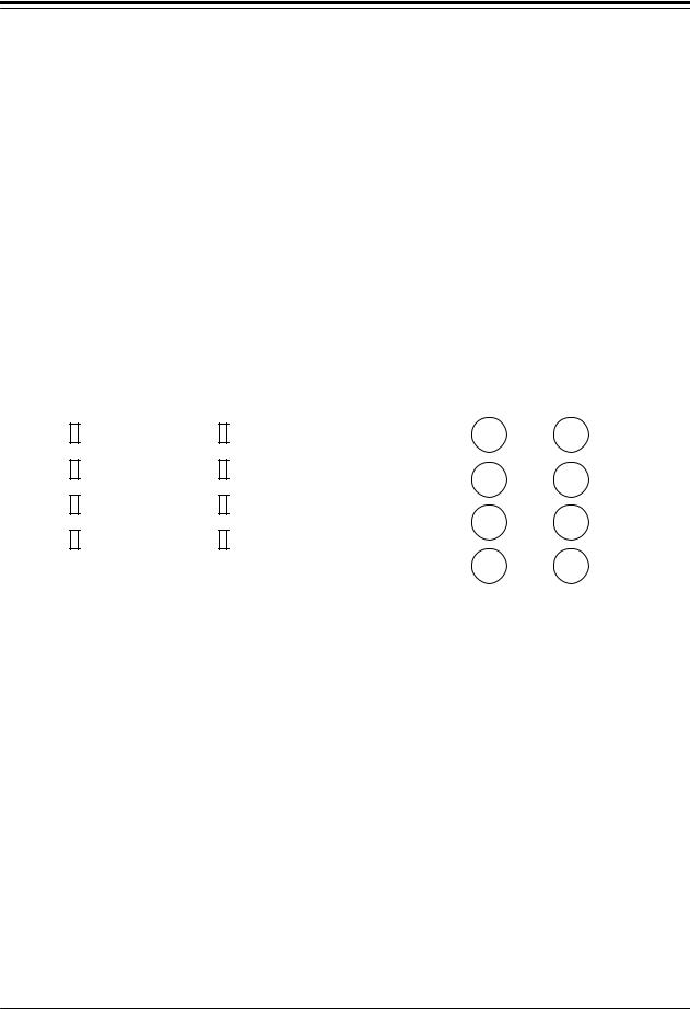
AT24C01C/AT24C02C
Package Types (not to scale)
1.Package Types (not to scale)
8-lead PDIP/SOIC/TSSOP
(Top View)
A0 |
|
1 |
8 |
|
Vcc |
|
|
5-lead SOT23(1) |
|
|
|
|
|
|
|
|
|||||||
|
|
|
|
|
(Top View) |
|
|
||||
|
|
|
|
|
|
|
|
|
|
|
|
|
|
|
|
|
|
|
|
|
|
|
WP |
A1 |
|
2 |
7 |
|
WP |
SCL |
|
1 |
5 |
|
|
|
|
|
|
||||||||
A2 |
|
3 |
6 |
|
SCL |
GND |
|
2 |
|
|
|
|
|
|
|
|
|
||||||
|
|
|
|
|
|
||||||
GND |
|
4 |
5 |
|
SDA |
SDA |
|
3 |
4 |
|
Vcc |
|
|
|
|
||||||||
|
|
|
|
||||||||
|
|
|
|
|
|
|
|
|
|
|
|
|
|
|
|
|
|
|
|
|
|
|
|
|
|
|
|
|
|
|
|
|
|
|
|
|
|
8-pad UDFN |
|
|
|
|
8-ball VFBGA |
|
|
|
|
(Top View) |
|
|
|
|
(Top View) |
|
|
|
|
|
|
|
|
|
|
|
|
A0 |
|
1 |
8 |
|
Vcc |
A0 |
1 |
8 |
Vcc |
A1 |
|
2 |
7 |
|
WP |
A1 |
2 |
7 |
WP |
|
|
||||||||
A2 |
|
3 |
6 |
|
SCL |
||||
|
|
A2 |
3 |
6 |
SCL |
||||
|
|
||||||||
GND |
|
4 |
5 |
|
SDA |
||||
|
|
||||||||
|
|
|
|
|
|
||||
|
|
|
|
|
|
GND |
4 |
5 |
SDA |
|
|
|
|
|
|
||||
|
|
|
|
|
|
||||
|
|
|
|
|
|
|
|
|
|
Note:
1.Refer to Device Addressing for details about addressing the SOT23 version of the device.
© 2018 Microchip Technology Inc. |
Datasheet |
DS20006111A-page 4 |