


Nexperia |
74HC595; 74HCT595 |
|
|
|
|
|
8-bit serial-in, serial or parallel-out shift register with output latches; 3-state |
11 Dynamic characteristics
Table 7. Dynamic characteristics
Voltages are referenced to GND (ground = 0 V); for test circuit see Figure 13.
Symbol |
Parameter |
|
Conditions |
|
|
|
25 °C |
|
-40 °C to |
-40 °C to |
Unit |
||||
|
|
|
|
|
|
|
|
|
|
|
+85 °C |
+125 °C |
|
||
|
|
|
|
|
|
|
|
Min |
Typ [1] |
Max |
Min |
Max |
Min |
Max |
|
74HC595 |
|
|
|
|
|
|
|
|
|
|
|
|
|
|
|
tpd |
propagation |
|
SHCP to Q7S; see Figure 8 |
[2] |
|
|
|
|
|
|
|
|
|||
|
|
|
|
|
|
|
|
|
|
||||||
|
delay |
|
|
|
|
|
|
|
|
|
|
|
|
|
|
|
|
|
|
VCC = 2 V |
|
|
- |
52 |
160 |
- |
200 |
- |
240 |
ns |
|
|
|
|
|
|
|
|
|||||||||
|
|
|
|
|
VCC = 4.5 V |
|
|
- |
19 |
32 |
- |
40 |
- |
48 |
ns |
|
|
|
|
|
VCC = 6 V |
|
|
- |
15 |
27 |
- |
34 |
- |
41 |
ns |
|
|
|
STCP to Qn; see Figure 9 |
[2] |
|
|
|
|
|
|
|
|
|||
|
|
|
|
|
|
|
|
|
|
|
|
||||
|
|
|
|
|
|
|
|
|
|
|
|
|
|
|
|
|
|
|
|
|
VCC = 2 V |
|
|
- |
55 |
175 |
- |
220 |
- |
265 |
ns |
|
|
|
|
|
VCC = 4.5 V |
|
|
- |
20 |
35 |
- |
44 |
- |
53 |
ns |
|
|
|
|
|
VCC = 6 V |
|
|
- |
16 |
30 |
- |
37 |
- |
45 |
ns |
tPHL |
HIGH |
|
|
|
to Q7S; see Figure 11 |
|
|
|
|
|
|
|
|
|
|
|
MR |
|
|
|
|
|
|
|
|
|
|||||
|
to LOW |
|
|
|
|
|
|
|
|
|
|
|
|
|
|
|
|
|
|
VCC = 2 V |
|
|
- |
47 |
175 |
- |
220 |
- |
265 |
ns |
|
|
propagation |
|
|
|
|
|
|||||||||
|
delay |
|
|
|
VCC = 4.5 V |
|
|
- |
17 |
35 |
- |
44 |
- |
53 |
ns |
|
|
|
|
|
VCC = 6 V |
|
|
- |
14 |
30 |
- |
37 |
- |
45 |
ns |
|
|
|
|
|
|
|
[3] |
|
|
|
|
|
|
|
|
ten |
enable time |
|
OE to Qn; see Figure 12 |
|
|
|
|
|
|
|
|
||||
|
|
|
|
|
|
|
|
|
|
||||||
|
|
|
|
|
VCC = 2 V |
|
|
- |
47 |
150 |
- |
190 |
- |
225 |
ns |
|
|
|
|
|
VCC = 4.5 V |
|
|
- |
17 |
30 |
- |
38 |
- |
45 |
ns |
|
|
|
|
|
VCC = 6 V |
|
|
- |
14 |
26 |
- |
33 |
- |
38 |
ns |
|
|
|
|
|
|
|
[4] |
|
|
|
|
|
|
|
|
tdis |
disable time |
|
OE to Qn; see Figure 12 |
|
|
|
|
|
|
|
|
||||
|
|
|
|
|
|
|
|
|
|
||||||
|
|
|
|
|
VCC = 2 V |
|
|
- |
41 |
150 |
- |
190 |
- |
225 |
ns |
|
|
|
|
|
VCC = 4.5 V |
|
|
- |
15 |
30 |
- |
38 |
- |
45 |
ns |
|
|
|
|
|
VCC = 6 V |
|
|
- |
12 |
27 |
- |
33 |
- |
38 |
ns |
tW |
pulse width |
|
SHCP HIGH or LOW; |
|
|
|
|
|
|
|
|
|
|||
|
|
|
see Figure 8 |
|
|
|
|
|
|
|
|
|
|
||
|
|
|
|
|
|
|
|
|
|
|
|
|
|
|
|
|
|
|
|
|
VCC = 2 V |
|
|
75 |
17 |
- |
95 |
- |
110 |
- |
ns |
|
|
|
|
|
VCC = 4.5 V |
|
|
15 |
6 |
- |
19 |
- |
22 |
- |
ns |
|
|
|
|
|
VCC = 6 V |
|
|
13 |
5 |
- |
16 |
- |
19 |
- |
ns |
|
|
|
STCP HIGH or LOW; |
|
|
|
|
|
|
|
|
|
|||
|
|
|
see Figure 9 |
|
|
|
|
|
|
|
|
|
|
||
|
|
|
|
|
|
|
|
|
|
|
|
|
|
|
|
|
|
|
|
|
VCC = 2 V |
|
|
75 |
11 |
- |
95 |
- |
110 |
- |
ns |
|
|
|
|
|
VCC = 4.5 V |
|
|
15 |
4 |
- |
19 |
- |
22 |
- |
ns |
|
|
|
|
|
VCC = 6 V |
|
|
13 |
3 |
- |
16 |
- |
19 |
- |
ns |
|
|
|
|
LOW; see Figure 11 |
|
|
|
|
|
|
|
|
|
||
|
|
|
MR |
|
|
|
|
|
|
|
|
|
|||
74HC_HCT595 |
|
|
|
|
|
All information provided in this document is subject to legal disclaimers. |
|
|
© Nexperia B.V. 2017. All rights reserved. |
||||||
Product data sheet |
|
|
|
|
Rev. 9 — 28 February 2017 |
|
|
|
|
|
9 / 22 |
||||
|
|
|
|
|
|
|
|
|
|
|
|
|
|
|
|
Nexperia |
|
|
|
|
|
|
74HC595; 74HCT595 |
|||||||
|
|
|
|
|
|
|
|
|
|
|
|
|
||
|
|
|
|
|
|
|
|
|
|
|
|
|
|
|
|
|
|
|
|
8-bit serial-in, serial or parallel-out shift register with output latches; 3-state |
|||||||||
|
|
|
|
|
|
|
|
|
|
|
|
|
|
|
Symbol |
Parameter |
|
Conditions |
|
|
25 °C |
|
-40 °C to |
-40 °C to |
Unit |
||||
|
|
|
|
|
|
|
|
|
|
+85 °C |
+125 °C |
|
||
|
|
|
|
|
|
|
Min |
Typ [1] |
Max |
Min |
Max |
Min |
Max |
|
|
|
|
|
|
VCC = 2 V |
|
75 |
17 |
- |
95 |
- |
110 |
- |
ns |
|
|
|
|
|
VCC = 4.5 V |
|
15 |
6 |
- |
19 |
- |
22 |
- |
ns |
|
|
|
|
|
VCC = 6 V |
|
13 |
5 |
- |
16 |
- |
19 |
- |
ns |
tsu |
set-up time |
|
DS to SHCP; see Figure 10 |
|
|
|
|
|
|
|
|
|
||
|
|
|
|
|
|
|
|
|
|
|
|
|
|
|
|
|
|
|
|
VCC = 2 V |
|
50 |
11 |
- |
65 |
- |
75 |
- |
ns |
|
|
|
|
|
VCC = 4.5 V |
|
10 |
4 |
- |
13 |
- |
15 |
- |
ns |
|
|
|
|
|
VCC = 6 V |
|
9 |
3 |
- |
11 |
- |
13 |
- |
ns |
|
|
|
SHCP to STCP; |
|
|
|
|
|
|
|
|
|
||
|
|
|
see Figure 10 |
|
|
|
|
|
|
|
|
|
||
|
|
|
|
|
|
|
|
|
|
|
|
|
|
|
|
|
|
|
|
VCC = 2 V |
|
75 |
22 |
- |
95 |
- |
110 |
- |
ns |
|
|
|
|
|
VCC = 4.5 V |
|
15 |
8 |
- |
19 |
- |
22 |
- |
ns |
|
|
|
|
|
VCC = 6 V |
|
13 |
7 |
- |
16 |
- |
19 |
- |
ns |
th |
hold time |
|
DS to SHCP; see Figure 10 |
|
|
|
|
|
|
|
|
|
||
|
|
|
|
|
|
|
|
|
|
|
|
|
|
|
|
|
|
|
|
VCC = 2 V |
|
3 |
-6 |
- |
3 |
- |
3 |
- |
ns |
|
|
|
|
|
VCC = 4.5 V |
|
3 |
-2 |
- |
3 |
- |
3 |
- |
ns |
|
|
|
|
|
VCC = 6 V |
|
3 |
-2 |
- |
3 |
- |
3 |
- |
ns |
trec |
recovery |
|
|
|
to SHCP; see Figure 11 |
|
|
|
|
|
|
|
|
|
|
MR |
|
|
|
|
|
|
|
|
|
||||
|
time |
|
|
|
|
|
|
|
|
|
|
|
|
|
|
|
|
|
VCC = 2 V |
|
50 |
-19 |
- |
65 |
- |
75 |
- |
ns |
|
|
|
|
|
|
|
|||||||||
|
|
|
|
|
VCC = 4.5 V |
|
10 |
-7 |
- |
13 |
- |
15 |
- |
ns |
|
|
|
|
|
VCC = 6 V |
|
9 |
-6 |
- |
11 |
- |
13 |
- |
ns |
fmax |
maximum |
|
SHCP or STCP; see Figure 8 |
|
|
|
|
|
|
|
|
|
||
|
frequency |
|
and Figure 9 |
|
|
|
|
|
|
|
|
|
||
|
|
|
|
|
VCC = 2 V |
|
9 |
30 |
- |
4.8 |
- |
4 |
- |
MHz |
|
|
|
|
|
VCC = 4.5 V |
|
30 |
91 |
- |
24 |
- |
20 |
- |
MHz |
|
|
|
|
|
VCC = 6 V |
|
35 |
108 |
- |
28 |
- |
24 |
- |
MHz |
CPD |
power |
|
fi = 1 MHz; VI = GND to VCC |
[5] [6] |
- |
115 |
- |
- |
- |
- |
- |
pF |
||
|
|
|||||||||||||
|
dissipation |
|
|
|
|
|
|
|
|
|
|
|
|
|
|
capacitance |
|
|
|
|
|
|
|
|
|
|
|
|
|
|
|
|
|
|
|
|
|
|
|
|
|
|
|
|
74HCT595; VCC = 4.5 V to 5.5 V |
|
|
|
|
|
|
|
|
|
|||||
tpd |
propagation |
|
SHCP to Q7S; see Figure 8 |
[2] |
- |
25 |
42 |
- |
53 |
- |
63 |
ns |
||
|
|
|||||||||||||
|
delay |
|
|
|
|
|
|
|
|
|
|
|
|
|
|
|
STCP to Qn; see Figure 9 |
[2] |
- |
24 |
40 |
- |
50 |
- |
60 |
ns |
|||
|
|
|
|
|||||||||||
|
|
|
|
|
|
|
|
|
|
|
|
|
|
|
tPHL |
HIGH |
|
|
|
to Q7S; see Figure 11 |
|
- |
23 |
40 |
- |
50 |
- |
60 |
ns |
|
MR |
|
||||||||||||
|
to LOW |
|
|
|
|
|
|
|
|
|
|
|
|
|
|
propagation |
|
|
|
|
|
|
|
|
|
|
|
|
|
|
delay |
|
|
|
|
|
|
|
|
|
|
|
|
|
|
|
|
|
|
|
|
|
|
|
|
|
|
|
|
|
|
|
|
|
|
[3] |
|
|
|
|
|
|
|
|
ten |
enable time |
|
OE to Qn; see Figure 12 |
- |
21 |
35 |
- |
44 |
- |
53 |
ns |
|||
|
|
|||||||||||||
|
|
|
|
|
|
[4] |
|
|
|
|
|
|
|
|
tdis |
disable time |
|
OE to Qn; see Figure 12 |
- |
18 |
30 |
- |
38 |
- |
45 |
ns |
|||
|
|
|||||||||||||
74HC_HCT595 |
|
|
|
|
All information provided in this document is subject to legal disclaimers. |
|
|
© Nexperia B.V. 2017. All rights reserved. |
||||||
Product data sheet |
|
|
|
Rev. 9 — 28 February 2017 |
|
|
|
|
|
10 / 22 |
||||
|
|
|
|
|
|
|
|
|
|
|
|
|
|
|
Nexperia |
|
|
|
|
|
74HC595; 74HCT595 |
|||||||
|
|
|
|
|
|
|
|
|
|
|
|
||
|
|
|
|
|
|
|
|
|
|
|
|
|
|
|
|
|
|
8-bit serial-in, serial or parallel-out shift register with output latches; 3-state |
|||||||||
|
|
|
|
|
|
|
|
|
|
|
|
|
|
Symbol |
Parameter |
|
Conditions |
|
|
25 °C |
|
-40 °C to |
-40 °C to |
Unit |
|||
|
|
|
|
|
|
|
|
|
+85 °C |
+125 °C |
|
||
|
|
|
|
|
|
Min |
Typ [1] |
Max |
Min |
Max |
Min |
Max |
|
tW |
pulse width |
|
SHCP HIGH or LOW; |
|
16 |
6 |
- |
20 |
- |
24 |
- |
ns |
|
|
|
|
see Figure 8 |
|
|
|
|
|
|
|
|
|
|
|
|
|
|
|
|
|
|
|
|
|
|
|
|
|
|
|
STCP HIGH or LOW; |
|
16 |
5 |
- |
20 |
- |
24 |
- |
ns |
|
|
|
|
see Figure 9 |
|
|
|
|
|
|
|
|
|
|
|
|
|
|
|
|
|
|
|
|
|
|
|
|
|
|
|
|
LOW; see Figure 11 |
|
20 |
8 |
- |
25 |
- |
30 |
- |
ns |
|
|
|
MR |
|
|||||||||
tsu |
set-up time |
|
DS to SHCP; see Figure 9 |
|
16 |
5 |
- |
20 |
- |
24 |
- |
ns |
|
|
|
|
|
|
|
|
|
|
|
|
|
|
|
|
|
|
SHCP to STCP; |
|
16 |
8 |
- |
20 |
- |
24 |
- |
ns |
|
|
|
|
see Figure 9 |
|
|
|
|
|
|
|
|
|
|
|
|
|
|
|
|
|
|
|
|
|
|
|
|
th |
hold time |
|
DS to SHCP; see Figure 10 |
|
3 |
-2 |
- |
3 |
- |
3 |
- |
ns |
|
trec |
recovery |
|
|
to SHCP; see Figure 11 |
|
10 |
-7 |
- |
13 |
- |
15 |
- |
ns |
|
MR |
|
|||||||||||
|
time |
|
|
|
|
|
|
|
|
|
|
|
|
|
|
|
|
|
|
|
|
|
|
|
|
|
|
fmax |
maximum |
|
SHCP and STCP; |
|
30 |
52 |
- |
24 |
- |
20 |
- |
MHz |
|
|
frequency |
|
see Figure 8 and Figure 9 |
|
|
|
|
|
|
|
|
|
|
|
|
|
|
|
|
|
|
|
|
|
|
|
|
CPD |
power |
|
fi = 1 MHz; |
[5] [6] |
- |
130 |
- |
- |
- |
- |
- |
pF |
|
|
|
||||||||||||
|
dissipation |
|
VI = GND to VCC - 1.5 V |
|
|
|
|
|
|
|
|
|
|
|
capacitance |
|
|
|
|
|
|
|
|
|
|
|
|
|
|
|
|
|
|
|
|
|
|
|
|
|
|
[1]Typical values are measured at nominal supply voltage.
[2]tpd is the same as tPHL and tPLH.
[3]ten is the same as tPZL and tPZH.
[4]tdis is the same as tPLZ and tPHZ.
[5]CPD is used to determine the dynamic power dissipation (PD in μW). PD = CPD × VCC2 × fi + Σ(CL × VCC2 × fo) where:
fi = input frequency in MHz;
fo = output frequency in MHz; Σ(CL × VCC2 × fo) = sum of outputs;
CL = output load capacitance in pF; VCC = supply voltage in V.
[6]All 9 outputs switching.
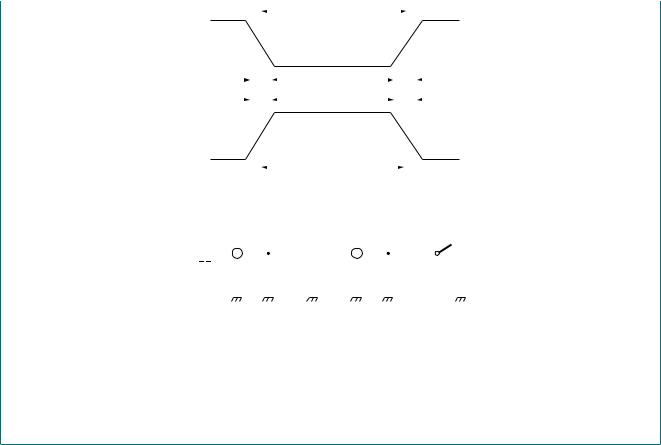
11.1Waveforms and test circuit
|
|
1/fmax |
VI |
|
|
SHCP input |
VM |
|
GND |
|
|
|
tW |
|
|
tPLH |
tPHL |
VOH |
|
|
Q7S output |
|
VM |
|
|
|
|
|||
VOL |
|
|
|
mna557 |
|
|
|
|
Measurement points are given in Table 8.
VOL and VOH are typical output voltage levels that occur with the output load.
Figure 8. Shift clock pulse, maximum frequency and input to output propagation delays
74HC_HCT595 |
All information provided in this document is subject to legal disclaimers. |
© Nexperia B.V. 2017. All rights reserved. |
Product data sheet |
Rev. 9 — 28 February 2017 |
|
11 / 22

Nexperia |
74HC595; 74HCT595 |
|
|
|
|
|
8-bit serial-in, serial or parallel-out shift register with output latches; 3-state |
VI |
|
|
|
|
|
|
|
|
|
SHCP input |
|
|
VM |
|
|
|
|||
GND |
|
|
|
|
|
tsu |
VI |
|
STCP input |
VM |
GND |
|
|
tW |
|
tPLH |
VOH
Qn output |
|
VM |
|
1/fmax
 tPHL
tPHL 
VOL
mna558
Measurement points are given in Table 8.
VOL and VOH are typical output voltage levels that occur with the output load.
Figure 9. Storage clock to output propagation delays
VI |
|
|
|
SHCP input |
|
VM |
|
|
|||
GND |
|
|
|
|
|
|
|
tsu |
tsu |
th |
th |
VI
DS input |
|
|
|
VM |
|
|
|
|
|
|
|
|
|
|
|
|
|
|
|
||||||
|
GND |
|||||||||||
Q7S output |
VOH |
|
|
|
|
|
|
VM |
||||
|
|
|
|
|
|
|||||||
|
|
|
|
|
|
|
||||||
|
|
|
|
|
|
|
||||||
|
VOL |
|||||||||||
|
|
|
|
|
|
|
|
|
|
mna560 |
||
Measurement points are given in Table 8.
The shaded areas indicate when the input is permitted to change for predictable output performance. VOL and VOH are typical output voltage levels that occur with the output load.
Figure 10. Data set-up and hold times
74HC_HCT595 |
All information provided in this document is subject to legal disclaimers. |
© Nexperia B.V. 2017. All rights reserved. |
Product data sheet |
Rev. 9 — 28 February 2017 |
12 / 22 |
|
|

Nexperia |
74HC595; 74HCT595 |
|
|
|
|
|
8-bit serial-in, serial or parallel-out shift register with output latches; 3-state |
MR input
SHCP input
Q7S output
VI |
|
VM |
|
GND |
|
tW |
trec |
VI |
|
|
VM |
GND |
|
tPHL |
|
VOH
VM
VOL |
mna561 |
|
Measurement points are given in Table 8.
VOL and VOH are typical output voltage levels that occur with the output load.
Figure 11. Master reset to output propagation delays
|
|
|
|
|
|
|
|
|
|
|
|
|
|
tr |
|
|
|
|
|
|
|
|
|
|
|
|
|
|
|
|
|
|
tf |
|||||||||||||||
|
|
|
|
|
|
|
|
|
|
|
|
|
|
|
|
|
|
|
|
|
|
|
|
|
|
|
|
|
|
|
|
|||||||||||||||||
|
|
|
|
|
|
|
|
|
90 % |
|
|
|
|
|
|
|
|
|
|
|
|
|
|
|
|
|
|
|
|
|
|
|
|
|
|
|
|
|
|
|
|
|
||||||
|
|
|
|
|
|
|
|
|
|
|
|
|
|
|
|
|
|
|
|
|
|
|
|
|
|
|
|
|
|
|
|
|
|
|
|
|
|
|||||||||||
|
|
input |
|
|
|
|
|
|
|
|
VM |
|
|
|
|
|
|
|
|
|
|
|
|
|
|
|
|
|
|
|
|
|
|
|
|
|
|
|
|
|
||||||||
|
OE |
10 % |
|
|
|
|
|
|
|
|
|
|
|
|
|
|
|
|
|
|
|
|
|
|
|
|
|
|
|
|
|
|
|
|
|
|
||||||||||||
|
|
|
|
|
|
|
|
|
|
|
|
|
|
|
|
|
|
|
|
|
|
|
|
|
|
|
|
|
|
|
||||||||||||||||||
Qn output |
|
|
|
|
|
|
|
|
tPLZ |
|
|
|
|
|
|
|
|
|
|
|
|
|
|
|
|
|
|
|
|
tPZL |
|
|
|
|
|
|
|
|
||||||||||
|
|
|
|
|
|
|
|
|
|
|
|
|
|
|
|
|
|
|
|
|
|
|
|
|
|
|
|
|
|
|
|
|
|
|
|
|||||||||||||
|
|
|
|
|
|
|
|
|
|
|
|
|
|
|
|
|
|
|
|
|
|
|
|
|
|
|
|
|
|
|
|
|
|
|
|
|
|
|||||||||||
|
|
|
|
|
|
|
|
|
|
|
|
|
|
|
|
|
|
|
|
|
|
|
|
|
|
|
|
|
|
VM |
||||||||||||||||||
|
|
|
|
|
|
|
|
|
|
|
|
|
|
|
|
|
|
|
|
|
|
|
|
|
|
|
|
|
|
|
|
|
|
|
|
|
|
|
|
|||||||||
LOW-to-OFF |
|
|
|
|
|
|
|
|
|
|
|
|
|
|
|
|
|
|
|
|
|
|
|
|
|
|
|
|
|
|
|
|
|
|
|
|
|
|
|
|
||||||||
|
|
|
|
|
|
|
|
|
|
|
|
|
|
|
|
|
|
|
|
|
|
|
|
|
|
|
|
|
|
|
|
|
|
|
|
|
|
|
||||||||||
OFF-to-LOW |
|
|
|
|
|
|
|
|
|
|
|
|
|
|
|
|
|
|
|
10 % |
|
|
|
|
|
|
|
|
|
|
|
|
|
|
|
|
|
|
|
|
|
|
||||||
|
|
|
|
|
|
|
|
|
|
|
|
|
|
|
|
|
|
|
|
|
|
|
|
|
|
|
|
|
|
|
|
|
|
|
|
|
|
|
|
|
|
|
|
|||||
Qn output |
|
|
|
|
|
|
|
|
|
|
|
|
tPHZ |
|
|
|
|
|
|
|
|
90 % |
|
|
|
|
|
|
|
|
|
|
tPZH |
|
|
|
|
|
|
VM |
||||||||
|
|
|
|
|
|
|
|
|
|
|
|
|
|
|
|
|
|
|
|
|
|
|
|
|
|
|
|
|
|
|
|
|
|
|
|
|||||||||||||
|
|
|
|
|
|
|
|
|
|
|
|
|
|
|
|
|
|
|
|
|
|
|
|
|
|
|
|
|
|
|
|
|
|
|
|
|
|
|
|
|
|
|
||||||
|
|
|
|
|
|
|
|
|
|
|
|
|
|
|
|
|
|
|
|
|
|
|
|
|
|
|
|
|
|
|
|
|
|
|
|
|
|
|||||||||||
|
|
|
|
|
|
|
|
|
|
|
|
|
|
|
|
|
|
|
|
|
|
|
|
|
|
|
|
|
|
|
|
|
|
|
|
|
|
|
|
|
|
|
|
|||||
HIGH-to-OFF |
|
|
|
|
|
|
|
|
|
|
|
|
|
|
|
|
|
|
|
|
|
|
|
|
|
|
|
|
|
|
|
|
|
|
|
|
|
|
|
|
|
|
|
|
||||
|
|
|
|
|
|
|
|
|
|
|
|
|
|
|
|
|
|
|
|
|
|
|
|
|
|
|
|
|
|
|
|
|
|
|
|
|
|
|
|
|
|
|
|
|||||
OFF-to-HIGH |
|
|
|
|
|
|
|
|
|
|
|
|
|
|
|
|
|
|
|
|
|
|
|
|
|
|
|
|
|
|
|
|
|
|
|
|
|
|
|
|
|
|
|
|
|
|
||
|
|
|
|
|
|
|
|
|
|
|
|
|
|
|
|
|
|
|
|
|
|
|
|
|
|
|
|
|
|
|
|
|
|
|
|
|
|
|
|
|
outputs |
|||||||
|
|
|
|
|
|
|
|
|
|
|
|
outputs |
|
|
|
|
|
|
|
outputs |
|
|
|
|
|
|
|
|
|
|
|
|
|
|
||||||||||||||
|
|
|
|
|
|
|
|
|
|
|
|
enabled |
|
|
|
|
|
|
|
|
disabled |
|
|
|
|
|
|
|
|
|
|
|
|
|
|
enabled |
||||||||||||
|
|
|
|
|
|
|
|
|
|
|
|
|
|
|
|
|
|
|
|
|
|
|
|
|
|
|
|
|
|
|
|
|
|
|
|
|
|
|
|
|
|
|
|
|
|
|
|
msa697 |
Measurement points are given in Table 8.
VOL and VOH are typical output voltage levels that occur with the output load.
Figure 12. Enable and disable times
Table 8. Measurement points
Type |
Input |
Output |
|
VM |
VM |
74HC595 |
0.5VCC |
0.5VCC |
74HCT595 |
1.3 V |
1.3 V |
|
|
|
74HC_HCT595 |
All information provided in this document is subject to legal disclaimers. |
© Nexperia B.V. 2017. All rights reserved. |
Product data sheet |
Rev. 9 — 28 February 2017 |
13 / 22 |
|
|
Nexperia |
|
|
|
|
|
|
|
|
|
|
|
|
|
|
|
|
|
|
|
|
|
|
|
|
|
|
|
|
|
|
|
|
74HC595; 74HCT595 |
|||||||||||||||||
|
|
|
|
|
|
|
|
|
|
|
|
|
|
|
|
|
|
|
|
|
|
|
|
|
|
|
|
|
|
|
|
|
|
|
|
|
|
|
|
|
|
|
|
|||||||
|
|
|
|
|
|
|
|
|
|
|
|
|
|
|
|
|
|
|
|
|
|
|
|
|
|
|
|
|
|
|
|
|
|
|
|
|
|
|
|
|
|
|
|
|
|
|
|
|
||
8-bit serial-in, serial or parallel-out shift register with output latches; 3-state |
||||||||||||||||||||||||||||||||||||||||||||||||||
|
|
|
|
|
|
|
|
|
|
|
|
|
|
|
|
|
|
|
|
|
|
|
|
|
|
|
|
|
|
|
|
|
|
|
|
|
|
|
|
|
|
|
|
|
|
|
|
|
|
|
|
VI |
90 % |
|
|
|
|
|
|
|
|
|
|
|
|
|
|
|
tW |
|
|
|
|
|
|
|
|
|
|
|
|
|
|
|
|
|
|
|
|
|
|
||||||||||
|
|
|
|
|
|
|
|
|
|
|
|
|
|
|
|
|
|
|
|
|
|
|
|
|
|
|
|
|
|
|
|
|
|
|
|
|
|
|||||||||||||
|
|
|
|
|
|
|
|
|
|
|
|
|
|
|
|
|
|
|
|
|
|
|
|
|
|
|
|
|
|
|
|
|
|
|
|
|
|
|
|
|||||||||||
negative |
|
|
|
|
|
|
|
VM |
|
|
|
|
|
|
|
VM |
|
|
|
|
|
|
|
|
|
|
|
|
||||||||||||||||||||||
|
|
|
|
|
|
|
|
|
|
|
|
|
|
|
|
|
|
|
|
|
|
|
|
|
|
|
|
|
|
|
||||||||||||||||||||
pulse |
|
|
|
|
|
|
|
|
|
|
|
|
|
|
|
|
|
|
|
|
|
|
|
|
|
|
|
|
|
|
|
|||||||||||||||||||
|
|
|
|
|
|
|
|
|
|
|
|
|
|
|
|
|
|
|
||||||||||||||||||||||||||||||||
|
|
|
|
|
|
|
|
|
|
|
|
|
|
|
|
|
|
|
|
|||||||||||||||||||||||||||||||
0 V |
|
|
|
|
|
|
|
|
|
|
|
|
10 % |
|
|
|
|
|
|
|
|
|
|
|
|
|
|
|
|
|
|
|
|
|
|
|
|
|
||||||||||||
|
|
|
|
|
|
|
|
|
|
|
|
|
|
|
|
|
|
|
|
|
|
|
|
|
|
|
|
|
|
|
|
|
||||||||||||||||||
|
|
|
|
|
|
|
|
|
|
|
|
|
|
|
|
|
|
|
|
|
|
|
|
|
|
|
|
|
|
|
|
|
|
|
|
|
|
|
|
|
|
|
|
|||||||
|
|
|
|
|
|
|
|
|
|
tf |
|
|
|
|
|
|
|
|
|
|
|
|
|
|
|
|
|
|
tr |
|
|
|
|
|
|
|||||||||||||||
|
|
|
|
|
|
|
|
|
|
|
|
|
|
|
|
|
|
|
|
|
|
|
|
|
|
|
|
|
|
|
|
|
|
|
|
|
|
|
|
|
||||||||||
|
|
|
|
|
|
|
|
|
|
|
|
|
|
|
|
|
|
|
|
|
|
|
|
|
|
|
|
|
|
|
|
|
|
|
|
|
|
|
|
|
||||||||||
|
VI |
|
|
|
|
|
|
|
|
|
|
|
tr |
|
|
|
|
|
|
|
|
|
|
|
|
|
|
|
|
|
|
tf |
|
|
|
|
|
|
||||||||||||
|
|
|
|
|
|
|
|
|
|
|
|
|
|
90 % |
|
|
|
|
|
|
|
|
|
|
|
|
|
|
|
|
|
|
|
|||||||||||||||||
|
|
|
|
|
|
|
|
|
|
|
|
|
|
|
|
|
|
|
|
|
|
|
|
|
|
|
|
|
|
|
|
|
|
|
|
|
|
|
|
|
|
|
||||||||
positive |
|
|
|
|
|
|
|
|
|
|
|
|
VM |
|
|
|
|
|
|
|
VM |
|
|
|
|
|
|
|
|
|
|
|
|
|||||||||||||||||
pulse |
10 % |
|
|
|
|
|
|
|
|
|
|
|
|
|
|
|
|
|
|
|
|
|
|
|
|
|
|
|||||||||||||||||||||||
0 V |
|
|
|
|
|
|
|
|
|
|
|
|
|
|
|
tW |
|
|
|
|
|
|
|
|
|
|
|
|
|
|
|
|
|
|
|
|
|
|||||||||||||
|
|
|
|
|
|
|
|
|
|
|
|
|
|
|
|
|
|
|
|
|
|
|
|
|
|
|
|
|
|
|
|
|
|
|
||||||||||||||||
|
|
|
|
|
|
|
|
|
|
|
|
|
|
|
|
|
|
|
|
|
|
|
|
|
|
|
|
|
|
|
|
|
|
|
|
|
|
|
|
|
||||||||||
|
|
|
|
|
|
|
|
|
|
|
|
|
|
|
|
|
|
|
|
|
|
|
|
|
|
|
|
|
|
|
|
|
|
|
|
|
|
|
|
|
|
|
|
|
|
|
|
|||
|
|
|
|
|
|
|
|
|
|
|
|
|
|
|
|
|
|
|
|
|
|
|
|
|
VCC |
|
|
|
|
|
|
|
|
|
|
|
|
|
|
|
|
|
|
|
VCC |
|||||
|
|
|
|
|
|
|
|
|
|
|
|
|
|
|
|
|
|
|
|
|
|
|
|
|
|
|
|
|
|
|
|
|
|
|
|
|
|
|
|
|
|
|
|
|
|
|
||||
|
|
|
|
|
|
|
|
|
VI |
|
|
|
|
|
|
VO |
|
|
|
|
|
|
|
R S1 |
|
|
||||||||||||||||||||||||
|
|
|
|
|
|
|
|
|
|
|
|
|
|
|
|
|
|
|
|
|
|
|
|
|||||||||||||||||||||||||||
|
G |
|
|
|
|
|
|
|
|
|
|
|
|
|
|
|
|
|
|
|
|
|
|
|
|
|
|
|
|
|
|
|
|
|
|
|
|
|
L |
|||||||||||
|
|
|
|
|
|
|
|
|
|
|
|
|
|
|
|
|
|
|
|
|
|
|
|
|
DUT |
|
|
|
|
|
|
|
|
|
|
|
|
|
|
|
|
|
|
|
|
|
|
|
open |
|
|
|
|
|
|
|
|
|
|
|
|
|
|
|
|
|
|
|
|
|
|
|
|
|
|
|
|
|
|
|
|
|
|
|
|
|
|
|
|
|
|
|
|
|
|
|
|
||||
|
|
|
|
|
|
|
|
|
|
|
|
|
|
|
|
|
|
|
|
|
|
RT |
|
|
|
|
|
|
|
|
|
|
|
|
CL |
|
||||||||||||||
|
|
|
|
|
|
|
|
|
|
|
|
|
|
|
|
|
|
|
|
|
|
|
|
|
|
|
|
|
|
|
|
|
|
|||||||||||||||||
|
|
|
|
|
|
|
|
|
|
|
|
|
|
|
|
|
|
|
|
|
|
|
|
|
|
|
|
|
|
|
|
|||||||||||||||||||
|
|
|
|
|
|
|
|
|
|
|
|
|
|
|
|
|
|
|
|
|
|
|
|
|
|
|
|
|
|
|
|
|
|
|
|
|
|
|
|
|
|
|
|
|
|
|
|
|
|
|
|
|
|
|
|
|
|
|
|
|
|
|
|
|
|
|
|
|
|
|
|
|
|
|
|
|
|
|
|
|
|
|
|
|
|
|
|
|
|
|
|
|
|
|
|
|
|
|
001aad983 |
||
Test data is given in Table 9. Definitions for test circuit:
CL = load capacitance including jig and probe capacitance. RL = load resistance.
RT = termination resistance should be equal to the output impedance Zo of the pulse generator. S1 = test selection switch.
Figure 13. Test circuit for measuring switching times
Table 9. Test data
Type |
Input |
|
Load |
|
S1 position |
|
|
|
VI |
tr, tf |
CL |
RL |
tPHL, tPLH |
tPZH, tPHZ |
tPZL, tPLZ |
74HC595 |
VCC |
6 ns |
50 pF |
1 kΩ |
open |
GND |
VCC |
|
|
|
|
|
|
|
|
74HCT595 |
3 V |
6 ns |
50 pF |
1 kΩ |
open |
GND |
VCC |
|
|
|
|
|
|
|
|
74HC_HCT595 |
All information provided in this document is subject to legal disclaimers. |
© Nexperia B.V. 2017. All rights reserved. |
Product data sheet |
Rev. 9 — 28 February 2017 |
14 / 22 |
|
|