

17.6.1Input Capture Trigger Source
The main trigger source for the input capture unit is the Input Capture Pin (ICPn). Timer/Counter1 can alternatively use the analog comparator output as trigger source for the input capture unit. The Analog Comparator is selected as trigger source by setting the analog Comparator Input Capture (ACIC) bit in the Analog Comparator Control and Status Register (ACSR). Be aware that changing trigger source can trigger a capture. The input capture flag must therefore be cleared after the change.
Both the Input Capture Pin (ICPn) and the Analog Comparator output (ACO) inputs are sampled using the same technique as for the Tn pin (Figure 18-1 on page 164). The edge detector is also identical. However, when the noise canceler is enabled, additional logic is inserted before the edge detector, which increases the delay by four system clock cycles. Note that the input of the noise canceler and edge detector is always enabled unless the Timer/Counter is set in a Waveform Generation mode that uses ICRn to define TOP.
An input capture can be triggered by software by controlling the port of the ICPn pin.
17.6.2Noise Canceler
The noise canceler improves noise immunity by using a simple digital filtering scheme. The noise canceler input is monitored over four samples, and all four must be equal for changing the output that in turn is used by the edge detector.
The noise canceler is enabled by setting the Input Capture Noise Canceler (ICNCn) bit in Timer/Counter Control Register B (TCCRnB). When enabled the noise canceler introduces additional four system clock cycles of delay from a change applied to the input, to the update of the ICRn Register. The noise canceler uses the system clock and is therefore not affected by the prescaler.
17.6.3Using the Input Capture Unit
The main challenge when using the Input Capture unit is to assign enough processor capacity for handling the incoming events. The time between two events is critical. If the processor has not read the captured value in the ICRn Register before the next event occurs, the ICRn will be overwritten with a new value. In this case the result of the capture will be incorrect.
When using the Input Capture interrupt, the ICRn Register should be read as early in the interrupt handler routine as possible. Even though the Input Capture interrupt has relatively high priority, the maximum interrupt response time is dependent on the maximum number of clock cycles it takes to handle any of the other interrupt requests.
Using the Input Capture unit in any mode of operation when the TOP value (resolution) is actively changed during operation, is not recommended.
Measurement of an external signal’s duty cycle requires that the trigger edge is changed after each capture. Changing the edge sensing must be done as early as possible after the ICRn Register has been read. After a change of the edge, the Input Capture Flag (ICFn) must be cleared by software (writing a logical one to the I/O bit location). For measuring frequency only, the clearing of the ICFn Flag is not required (if an interrupt handler is used).
17.7Output Compare Units
The 16-bit comparator continuously compares TCNTn with the Output Compare Register (OCRnx). If TCNT equals OCRnx the comparator signals a match. A match will set the Output Compare Flag (OCFnx) at the next timer clock cycle. If enabled (OCIEnx = 1), the Output Compare Flag generates an Output Compare interrupt. The OCFnx Flag is automatically cleared when the interrupt is executed. Alternatively the OCFnx Flag can be cleared by software by writing a logical one to its I/O bit location. The Waveform Generator uses the match signal to generate an output according to operating mode set by the Waveform Generation mode (WGMn3:0) bits and Compare Output mode (COMnx1:0) bits. The TOP and BOTTOM signals are used by the Waveform Generator for handling the special cases of the extreme values in some modes of operation. See “Modes of Operation” on page 144.
ATmega640/V-1280/V-1281/V-2560/V-2561/V [DATASHEET] |
141 |
2549Q–AVR–02/2014
A special feature of Output Compare unit A allows it to define the Timer/Counter TOP value (that is, counter resolution). In addition to the counter resolution, the TOP value defines the period time for waveforms generated by the Waveform Generator.
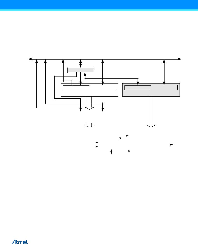
Figure 17-4 shows a block diagram of the Output Compare unit. The small “n” in the register and bit names indicates the device number (n = n for Timer/Counter n), and the “x” indicates Output Compare unit (A/B/C). The elements of the block diagram that are not directly a part of the Output Compare unit are gray shaded.
Figure 17-4. Output Compare Unit, Block Diagram |
|
|
|
|
DATA BUS (8-bit) |
|
|
TEMP (8-bit) |
|
|
|
OCRnxH Buf. (8-bit) |
OCRnxL Buf. (8-bit) |
TCNTnH (8-bit) |
TCNTnL (8-bit) |
OCRnx Buffer (16-bit Register) |
TCNTn (16-bit Counter) |
||
|
|
|
|
|
|
|
|
|
|
|
|
|
|
|
|
|
|
|
|
|
|
|
|
|
|
|
|
|
|
|
|
|
|
|
|
|
OCRnxH (8-bit) |
|
OCRnxL (8-bit) |
|
|
|
|
|
|
|
||||
|
|
|
|
|
|
|
|
|
|
|
|
|
|
|||
|
|
|
|
OCRnx (16-bit Register) |
|
|
|
|
|
|
|
|||||
|
|
|
|
|
|
|
|
|
|
|
|
|
|
|
|
|
|
|
|
|
|
|
|
|
|
|
|
|
|
|
|
|
|
|
|
|
|
|
|
|
|
= (16-bit Comparator ) |
|
|
|
|||||
|
|
|
|
|
|
|
|
|
|
|
|
OCFnx (Int.Req.) |
|
|
|
|
|
|
|
|
|
|
|
|
|
|
|
|
|
|
|
||
|
|
|
|
|
|
|
|
|
|
|
|
|
|
|
|
|
|
|
|
|
TOP |
|
|
|
Waveform Generator |
|
|
|
OCnx |
||||
|
|
|
|
|
|
|
||||||||||
|
|
|
BOTTOM |
|
|
|
|
|
|
|||||||
|
|
|
|
|
|
|
|
|
||||||||
|
|
|
|
|
|
|
|
|
|
|
|
|
|
|
||
|
|
|
|
|
|
|
|
|
|
|
|
|
|
|
||
|
|
|
|
|
|
|
|
|
|
|
|
|
|
|
|
|
WGMn3:0 COMnx1:0
The OCRnx Register is double buffered when using any of the twelve Pulse Width Modulation (PWM) modes. For the Normal and Clear Timer on Compare (CTC) modes of operation, the double buffering is disabled. The double buffering synchronizes the update of the OCRnx Compare Register to either TOP or BOTTOM of the counting sequence. The synchronization prevents the occurrence of odd-length, non-symmetrical PWM pulses, thereby making the output glitch-free.
The OCRnx Register access may seem complex, but this is not case. When the double buffering is enabled, the CPU has access to the OCRnx Buffer Register, and if double buffering is disabled the CPU will access the OCRnx directly. The content of the OCR1x (Buffer or Compare) Register is only changed by a write operation (the Timer/Counter does not update this register automatically as the TCNT1 and ICR1 Register). Therefore OCR1x is not read via the high byte temporary register (TEMP). However, it is a good practice to read the low byte first as when accessing other 16-bit registers. Writing the OCRnx Registers must be done via the TEMP Register since the compare of all 16 bits is done continuously. The high byte (OCRnxH) has to be written first. When the high byte I/O location is written by the CPU, the TEMP Register will be updated by the value written. Then when the low byte (OCRnxL) is written to the lower eight bits, the high byte will be copied into the upper 8-bits of either the OCRnx buffer or OCRnx Compare Register in the same system clock cycle.
For more information of how to access the 16-bit registers refer to “Accessing 16-bit Registers” on page 135.
ATmega640/V-1280/V-1281/V-2560/V-2561/V [DATASHEET] |
142 |
2549Q–AVR–02/2014