
- •1. Pin Configurations
- •2. Overview
- •2.1 Block Diagram
- •2.2 Comparison Between ATmega1281/2561 and ATmega640/1280/2560
- •2.3 Pin Descriptions
- •2.3.3 Port A (PA7..PA0)
- •2.3.4 Port B (PB7..PB0)
- •2.3.5 Port C (PC7..PC0)
- •2.3.6 Port D (PD7..PD0)
- •2.3.7 Port E (PE7..PE0)
- •2.3.8 Port F (PF7..PF0)
- •2.3.9 Port G (PG5..PG0)
- •2.3.10 Port H (PH7..PH0)
- •2.3.11 Port J (PJ7..PJ0)
- •2.3.12 Port K (PK7..PK0)
- •2.3.13 Port L (PL7..PL0)
- •2.3.14 RESET
- •2.3.15 XTAL1
- •2.3.16 XTAL2
- •2.3.17 AVCC
- •2.3.18 AREF
- •3. Resources
- •4. About Code Examples
- •5. Data Retention
- •6. Capacitive touch sensing
- •7. AVR CPU Core
- •7.1 Introduction
- •7.2 Architectural Overview
- •7.3 ALU – Arithmetic Logic Unit
- •7.4 Status Register
- •7.4.1 SREG – AVR Status Register
- •7.5 General Purpose Register File
- •7.6 Stack Pointer
- •7.6.2 EIND – Extended Indirect Register
- •7.7 Instruction Execution Timing
- •7.8 Reset and Interrupt Handling
- •7.8.1 Interrupt Response Time
- •8. AVR Memories
- •8.2 SRAM Data Memory
- •8.2.1 Data Memory Access Times
- •8.3 EEPROM Data Memory
- •8.3.1 EEPROM Read/Write Access
- •8.3.2 Preventing EEPROM Corruption
- •8.4 I/O Memory
- •8.4.1 General Purpose I/O Registers
- •9. External Memory Interface
- •9.1 Overview
- •9.1.1 Using the External Memory Interface
- •9.1.2 Address Latch Requirements
- •9.1.4 Timing
- •9.1.5 Using all Locations of External Memory Smaller than 64Kbytes
- •9.1.6 Using all 64Kbytes Locations of External Memory
- •9.2 Register Description
- •9.2.1 EEPROM registers
- •9.3 General Purpose registers
- •9.3.1 GPIOR2 – General Purpose I/O Register 2
- •9.3.2 GPIOR1 – General Purpose I/O Register 1
- •9.3.3 GPIOR0 – General Purpose I/O Register 0
- •9.4 External Memory registers
- •9.4.1 XMCRA – External Memory Control Register A
- •9.4.2 XMCRB – External Memory Control Register B
- •10. System Clock and Clock Options
- •10.1 Overview
- •10.2 Clock Systems and their Distribution
- •10.3 Clock Sources
- •10.3.1 Default Clock Source
- •10.4 Low Power Crystal Oscillator
- •10.5 Full Swing Crystal Oscillator
- •10.6 Low Frequency Crystal Oscillator
- •10.7 Calibrated Internal RC Oscillator
- •10.8 128kHz Internal Oscillator
- •10.9 External Clock
- •10.10 Clock Output Buffer
- •10.11 Timer/Counter Oscillator
- •10.12 System Clock Prescaler
- •10.13 Register Description
- •10.13.1 OSCCAL – Oscillator Calibration Register
- •10.13.2 CLKPR – Clock Prescale Register
- •11. Power Management and Sleep Modes
- •11.1 Sleep Modes
- •11.2 Idle Mode
- •11.3 ADC Noise Reduction Mode
- •11.6 Standby Mode
- •11.7 Extended Standby Mode
- •11.8 Power Reduction Register
- •11.9 Minimizing Power Consumption
- •11.9.1 Analog to Digital Converter
- •11.9.2 Analog Comparator
- •11.9.4 Internal Voltage Reference
- •11.9.5 Watchdog Timer
- •11.9.6 Port Pins
- •11.10 Register Description
- •11.10.1 SMCR – Sleep Mode Control Register
- •11.10.2 PRR0 – Power Reduction Register 0
- •11.10.3 PRR1 – Power Reduction Register 1
- •12. System Control and Reset
- •12.1 Resetting the AVR
- •12.2 Reset Sources
- •12.2.1 Power-on Reset
- •12.2.2 External Reset
- •12.2.4 Watchdog Reset
- •12.3 Internal Voltage Reference
- •12.4 Watchdog Timer
- •12.4.1 Features
- •12.4.2 Overview
- •12.5 Register Description
- •12.5.1 MCUSR – MCU Status Register
- •12.5.2 WDTCSR – Watchdog Timer Control Register
- •13. I/O-Ports
- •13.1 Introduction
- •13.2 Ports as General Digital I/O
- •13.2.1 Configuring the Pin
- •13.2.2 Toggling the Pin
- •13.2.3 Switching Between Input and Output
- •13.2.4 Reading the Pin Value
- •13.2.5 Digital Input Enable and Sleep Modes
- •13.2.6 Unconnected Pins
- •13.3 Alternate Port Functions
- •13.3.1 Alternate Functions of Port A
- •13.3.2 Alternate Functions of Port B
- •13.3.3 Alternate Functions of Port C
- •13.3.4 Alternate Functions of Port D
- •13.3.5 Alternate Functions of Port E
- •13.3.6 Alternate Functions of Port F
- •13.3.7 Alternate Functions of Port G
- •13.3.8 Alternate Functions of Port H
- •13.3.9 Alternate Functions of Port J
- •13.3.10 Alternate Functions of Port K
- •13.3.11 Alternate Functions of Port L
- •13.4.1 MCUCR – MCU Control Register
- •13.4.2 PORTA – Port A Data Register
- •13.4.3 DDRA – Port A Data Direction Register
- •13.4.4 PINA – Port A Input Pins Address
- •13.4.5 PORTB – Port B Data Register
- •13.4.6 DDRB – Port B Data Direction Register
- •13.4.7 PINB – Port B Input Pins Address
- •13.4.8 PORTC – Port C Data Register
- •13.4.9 DDRC – Port C Data Direction Register
- •13.4.10 PINC– Port C Input Pins Address
- •13.4.11 PORTD – Port D Data Register
- •13.4.12 DDRD – Port D Data Direction Register
- •13.4.13 PIND – Port D Input Pins Address
- •13.4.14 PORTE – Port E Data Register
- •13.4.15 DDRE – Port E Data Direction Register
- •13.4.16 PINE – Port E Input Pins Address
- •13.4.17 PORTF – Port F Data Register
- •13.4.18 DDRF – Port F Data Direction Register
- •13.4.19 PINF – Port F Input Pins Address
- •13.4.20 PORTG – Port G Data Register
- •13.4.21 DDRG – Port G Data Direction Register
- •13.4.22 PING – Port G Input Pins Address
- •13.4.23 PORTH – Port H Data Register
- •13.4.24 DDRH – Port H Data Direction Register
- •13.4.25 PINH – Port H Input Pins Address
- •13.4.26 PORTJ – Port J Data Register
- •13.4.27 DDRJ – Port J Data Direction Register
- •13.4.28 PINJ – Port J Input Pins Address
- •13.4.29 PORTK – Port K Data Register
- •13.4.30 DDRK – Port K Data Direction Register
- •13.4.31 PINK – Port K Input Pins Address
- •13.4.32 PORTL – Port L Data Register
- •13.4.33 DDRL – Port L Data Direction Register
- •13.4.34 PINL – Port L Input Pins Address
- •14. Interrupts
- •14.1 Interrupt Vectors in ATmega640/1280/1281/2560/2561
- •14.2 Reset and Interrupt Vector placement
- •14.3 Moving Interrupts Between Application and Boot Section
- •14.4 Register Description
- •14.4.1 MCUCR – MCU Control Register
- •15. External Interrupts
- •15.1 Pin Change Interrupt Timing
- •15.2 Register Description
- •15.2.1 EICRA – External Interrupt Control Register A
- •15.2.2 EICRB – External Interrupt Control Register B
- •15.2.3 EIMSK – External Interrupt Mask Register
- •15.2.4 EIFR – External Interrupt Flag Register
- •15.2.5 PCICR – Pin Change Interrupt Control Register
- •15.2.6 PCIFR – Pin Change Interrupt Flag Register
- •15.2.7 PCMSK2 – Pin Change Mask Register 2
- •15.2.8 PCMSK1 – Pin Change Mask Register 1
- •15.2.9 PCMSK0 – Pin Change Mask Register 0
- •16. 8-bit Timer/Counter0 with PWM
- •16.1 Features
- •16.2 Overview
- •16.2.1 Registers
- •16.2.2 Definitions
- •16.3 Timer/Counter Clock Sources
- •16.4 Counter Unit
- •16.5 Output Compare Unit
- •16.5.1 Force Output Compare
- •16.5.2 Compare Match Blocking by TCNT0 Write
- •16.5.3 Using the Output Compare Unit
- •16.6 Compare Match Output Unit
- •16.6.1 Compare Output Mode and Waveform Generation
- •16.7 Modes of Operation
- •16.7.1 Normal Mode
- •16.7.2 Clear Timer on Compare Match (CTC) Mode
- •16.7.3 Fast PWM Mode
- •16.7.4 Phase Correct PWM Mode
- •16.8 Timer/Counter Timing Diagrams
- •16.9 Register Description
- •16.9.1 TCCR0A – Timer/Counter Control Register A
- •16.9.2 TCCR0B – Timer/Counter Control Register B
- •16.9.3 TCNT0 – Timer/Counter Register
- •16.9.4 OCR0A – Output Compare Register A
- •16.9.5 OCR0B – Output Compare Register B
- •16.9.6 TIMSK0 – Timer/Counter Interrupt Mask Register
- •16.9.7 TIFR0 – Timer/Counter 0 Interrupt Flag Register
- •17. 16-bit Timer/Counter (Timer/Counter 1, 3, 4, and 5)
- •17.1 Features
- •17.2 Overview
- •17.2.1 Registers
- •17.2.2 Definitions
- •17.3.1 Reusing the Temporary High Byte Register
- •17.4 Timer/Counter Clock Sources
- •17.5 Counter Unit
- •17.6 Input Capture Unit
- •17.6.1 Input Capture Trigger Source
- •17.6.2 Noise Canceler
- •17.6.3 Using the Input Capture Unit
- •17.7 Output Compare Units
- •17.7.1 Force Output Compare
- •17.7.2 Compare Match Blocking by TCNTn Write
- •17.7.3 Using the Output Compare Unit
- •17.8 Compare Match Output Unit
- •17.8.1 Compare Output Mode and Waveform Generation
- •17.9 Modes of Operation
- •17.9.1 Normal Mode
- •17.9.2 Clear Timer on Compare Match (CTC) Mode
- •17.9.3 Fast PWM Mode
- •17.9.4 Phase Correct PWM Mode
- •17.9.5 Phase and Frequency Correct PWM Mode
- •17.10 Timer/Counter Timing Diagrams
- •17.11 Register Description
- •17.11.1 TCCR1A – Timer/Counter 1 Control Register A
- •17.11.2 TCCR3A – Timer/Counter 3 Control Register A
- •17.11.3 TCCR4A – Timer/Counter 4 Control Register A
- •17.11.4 TCCR5A – Timer/Counter 5 Control Register A
- •17.11.5 TCCR1B – Timer/Counter 1 Control Register B
- •17.11.6 TCCR3B – Timer/Counter 3 Control Register B
- •17.11.7 TCCR4B – Timer/Counter 4 Control Register B
- •17.11.8 TCCR5B – Timer/Counter 5 Control Register B
- •17.11.9 TCCR1C – Timer/Counter 1 Control Register C
- •17.11.10 TCCR3C – Timer/Counter 3 Control Register C
- •17.11.11 TCCR4C – Timer/Counter 4 Control Register C
- •17.11.12 TCCR5C – Timer/Counter 5 Control Register C
- •17.11.13 TCNT1H and TCNT1L – Timer/Counter 1
- •17.11.14 TCNT3H and TCNT3L – Timer/Counter 3
- •17.11.15 TCNT4H and TCNT4L –Timer/Counter 4
- •17.11.16 TCNT5H and TCNT5L –Timer/Counter 5
- •17.11.17 OCR1AH and OCR1AL – Output Compare Register 1 A
- •17.11.18 OCR1BH and OCR1BL – Output Compare Register 1 B
- •17.11.19 OCR1CH and OCR1CL – Output Compare Register 1 C
- •17.11.20 OCR3AH and OCR3AL – Output Compare Register 3 A
- •17.11.21 OCR3BH and OCR3BL – Output Compare Register 3 B
- •17.11.22 OCR3CH and OCR3CL – Output Compare Register 3 C
- •17.11.23 OCR4AH and OCR4AL – Output Compare Register 4 A
- •17.11.24 OCR4BH and OCR4BL – Output Compare Register 4 B
- •17.11.25 OCR4CH and OCR4CL –Output Compare Register 4 C
- •17.11.26 OCR5AH and OCR5AL – Output Compare Register 5 A
- •17.11.27 OCR5BH and OCR5BL – Output Compare Register 5 B
- •17.11.28 OCR5CH and OCR5CL –Output Compare Register 5 C
- •17.11.29 ICR1H and ICR1L – Input Capture Register 1
- •17.11.30 ICR3H and ICR3L – Input Capture Register 3
- •17.11.31 ICR4H and ICR4L – Input Capture Register 4
- •17.11.32 ICR5H and ICR5L – Input Capture Register 5
- •17.11.33 TIMSK1 – Timer/Counter 1 Interrupt Mask Register
- •17.11.34 TIMSK3 – Timer/Counter 3 Interrupt Mask Register
- •17.11.35 TIMSK4 – Timer/Counter 4 Interrupt Mask Register
- •17.11.36 TIMSK5 – Timer/Counter 5 Interrupt Mask Register
- •17.11.37 TIFR1 – Timer/Counter1 Interrupt Flag Register
- •17.11.38 TIFR3 – Timer/Counter3 Interrupt Flag Register
- •17.11.39 TIFR4 – Timer/Counter4 Interrupt Flag Register
- •17.11.40 TIFR5 – Timer/Counter5 Interrupt Flag Register
- •18. Timer/Counter 0, 1, 3, 4, and 5 Prescaler
- •18.1 Internal Clock Source
- •18.2 Prescaler Reset
- •18.3 External Clock Source
- •18.4 Register Description
- •18.4.1 GTCCR – General Timer/Counter Control Register
- •19. Output Compare Modulator (OCM1C0A)
- •19.1 Overview
- •19.2 Description
- •19.2.1 Timing example
- •20. 8-bit Timer/Counter2 with PWM and Asynchronous Operation
- •20.1 Overview
- •20.1.1 Registers
- •20.1.2 Definitions
- •20.2 Timer/Counter Clock Sources
- •20.3 Counter Unit
- •20.4 Modes of Operation
- •20.4.1 Normal Mode
- •20.4.2 Clear Timer on Compare Match (CTC) Mode
- •20.4.3 Fast PWM Mode
- •20.4.4 Phase Correct PWM Mode
- •20.5 Output Compare Unit
- •20.5.1 Force Output Compare
- •20.5.2 Compare Match Blocking by TCNT2 Write
- •20.5.3 Using the Output Compare Unit
- •20.6 Compare Match Output Unit
- •20.6.1 Compare Output Mode and Waveform Generation
- •20.7 Timer/Counter Timing Diagrams
- •20.8 Asynchronous Operation of Timer/Counter2
- •20.9 Timer/Counter Prescaler
- •20.10 Register Description
- •20.10.2 TCCR2B – Timer/Counter Control Register B
- •20.10.3 TCNT2 – Timer/Counter Register
- •20.10.4 OCR2A – Output Compare Register A
- •20.10.5 OCR2B – Output Compare Register B
- •20.10.6 ASSR – Asynchronous Status Register
- •20.10.7 TIMSK2 – Timer/Counter2 Interrupt Mask Register
- •20.10.8 TIFR2 – Timer/Counter2 Interrupt Flag Register
- •20.10.9 GTCCR – General Timer/Counter Control Register
- •21. SPI – Serial Peripheral Interface
- •21.1 SS Pin Functionality
- •21.1.1 Slave Mode
- •21.1.2 Master Mode
- •21.1.3 Data Modes
- •21.2 Register Description
- •21.2.1 SPCR – SPI Control Register
- •21.2.2 SPSR – SPI Status Register
- •21.2.3 SPDR – SPI Data Register
- •22. USART
- •22.1 Features
- •22.2 Overview
- •22.3 Clock Generation
- •22.3.1 Internal Clock Generation – The Baud Rate Generator
- •22.3.2 Double Speed Operation (U2Xn)
- •22.3.3 External Clock
- •22.3.4 Synchronous Clock Operation
- •22.4 Frame Formats
- •22.4.1 Parity Bit Calculation
- •22.5 USART Initialization
- •22.6 Data Transmission – The USART Transmitter
- •22.6.1 Sending Frames with 5 to 8 Data Bit
- •22.6.2 Sending Frames with 9 Data Bit
- •22.6.3 Transmitter Flags and Interrupts
- •22.6.4 Parity Generator
- •22.6.5 Disabling the Transmitter
- •22.7 Data Reception – The USART Receiver
- •22.7.1 Receiving Frames with 5 to 8 Data Bits
- •22.7.2 Receiving Frames with 9 Data Bits
- •22.7.3 Receive Compete Flag and Interrupt
- •22.7.4 Receiver Error Flags
- •22.7.5 Parity Checker
- •22.7.6 Disabling the Receiver
- •22.7.7 Flushing the Receive Buffer
- •22.8 Asynchronous Data Reception
- •22.8.1 Asynchronous Clock Recovery
- •22.8.2 Asynchronous Data Recovery
- •22.8.3 Asynchronous Operational Range
- •22.9.1 Using MPCMn
- •22.10 Register Description
- •22.10.1 UDRn – USART I/O Data Register n
- •22.10.2 UCSRnA – USART Control and Status Register A
- •22.10.3 UCSRnB – USART Control and Status Register n B
- •22.10.4 UCSRnC – USART Control and Status Register n C
- •22.10.5 UBRRnL and UBRRnH – USART Baud Rate Registers
- •22.11 Examples of Baud Rate Setting
- •23. USART in SPI Mode
- •23.1 Overview
- •23.2 USART MSPIM vs. SPI
- •23.2.1 Clock Generation
- •23.3 SPI Data Modes and Timing
- •23.4 Frame Formats
- •23.4.1 USART MSPIM Initialization
- •23.5 Data Transfer
- •23.5.1 Transmitter and Receiver Flags and Interrupts
- •23.5.2 Disabling the Transmitter or Receiver
- •23.6 USART MSPIM Register Description
- •23.6.1 UDRn – USART MSPIM I/O Data Register
- •23.6.2 UCSRnA – USART MSPIM Control and Status Register n A
- •23.6.3 UCSRnB – USART MSPIM Control and Status Register n B
- •23.6.4 UCSRnC – USART MSPIM Control and Status Register n C
- •23.6.5 UBRRnL and UBRRnH – USART MSPIM Baud Rate Registers
- •24. 2-wire Serial Interface
- •24.1 Features
- •24.2.1 TWI Terminology
- •24.2.2 Electrical Interconnection
- •24.3 Data Transfer and Frame Format
- •24.3.1 Transferring Bits
- •24.3.2 START and STOP Conditions
- •24.3.3 Address Packet Format
- •24.3.4 Data Packet Format
- •24.3.5 Combining Address and Data Packets into a Transmission
- •24.5 Overview of the TWI Module
- •24.5.1 SCL and SDA Pins
- •24.5.2 Bit Rate Generator Unit
- •24.5.3 Bus Interface Unit
- •24.5.4 Address Match Unit
- •24.5.5 Control Unit
- •24.6 Using the TWI
- •24.7 Transmission Modes
- •24.7.1 Master Transmitter Mode
- •24.7.2 Master Receiver Mode
- •24.7.3 Slave Receiver Mode
- •24.7.4 Slave Transmitter Mode
- •24.7.5 Miscellaneous States
- •24.7.6 Combining Several TWI Modes
- •24.9 Register Description
- •24.9.1 TWBR – TWI Bit Rate Register
- •24.9.2 TWCR – TWI Control Register
- •24.9.3 TWSR – TWI Status Register
- •24.9.4 TWDR – TWI Data Register
- •24.9.5 TWAR – TWI (Slave) Address Register
- •24.9.6 TWAMR – TWI (Slave) Address Mask Register
- •25. AC – Analog Comparator
- •25.1 Analog Comparator Multiplexed Input
- •25.2 Register Description
- •25.2.1 ADCSRB – ADC Control and Status Register B
- •25.2.2 ACSR – Analog Comparator Control and Status Register
- •25.2.3 DIDR1 – Digital Input Disable Register 1
- •26. ADC – Analog to Digital Converter
- •26.1 Features
- •26.2 Operation
- •26.3 Starting a Conversion
- •26.4 Prescaling and Conversion Timing
- •26.4.1 Differential Channels
- •26.5 Changing Channel or Reference Selection
- •26.5.1 ADC Input Channels
- •26.5.2 ADC Voltage Reference
- •26.6 ADC Noise Canceler
- •26.6.1 Analog Input Circuitry
- •26.6.2 Analog Noise Canceling Techniques
- •26.6.3 Offset Compensation Schemes
- •26.6.4 ADC Accuracy Definitions
- •26.7 ADC Conversion Result
- •26.8 Register Description
- •26.8.1 ADMUX – ADC Multiplexer Selection Register
- •26.8.2 ADCSRB – ADC Control and Status Register B
- •26.8.3 ADCSRA – ADC Control and Status Register A
- •26.8.4 ADCL and ADCH – The ADC Data Register
- •26.8.5 ADCSRB – ADC Control and Status Register B
- •26.8.6 DIDR0 – Digital Input Disable Register 0
- •26.8.7 DIDR2 – Digital Input Disable Register 2
- •27. JTAG Interface and On-chip Debug System
- •27.1 Features
- •27.2 Overview
- •27.3 TAP - Test Access Port
- •27.3.1 TAP Controller
- •27.6.1 PRIVATE0; 0x8
- •27.6.2 PRIVATE1; 0x9
- •27.6.3 PRIVATE2; 0xA
- •27.6.4 PRIVATE3; 0xB
- •27.7 Using the JTAG Programming Capabilities
- •27.8 Bibliography
- •28. IEEE 1149.1 (JTAG) Boundary-scan
- •28.1 Features
- •28.2 System Overview
- •28.3 Data Registers
- •28.3.1 Bypass Register
- •28.3.2 Device Identification Register
- •28.3.3 Reset Register
- •28.4.1 EXTEST; 0x0
- •28.4.2 IDCODE; 0x1
- •28.4.3 SAMPLE_PRELOAD; 0x2
- •28.4.4 AVR_RESET; 0xC
- •28.4.5 BYPASS; 0xF
- •28.5.1 Scanning the Digital Port Pins
- •28.5.2 Scanning the RESET Pin
- •28.6.1 MCUCR – MCU Control Register
- •28.6.2 MCUSR – MCU Status Register
- •29. Boot Loader Support – Read-While-Write Self-Programming
- •29.1 Features
- •29.2 Application and Boot Loader Flash Sections
- •29.2.1 Application Section
- •29.2.2 BLS – Boot Loader Section
- •29.4 Boot Loader Lock Bits
- •29.4.1 Entering the Boot Loader Program
- •29.6.1 Performing Page Erase by SPM
- •29.6.2 Filling the Temporary Buffer (Page Loading)
- •29.6.3 Performing a Page Write
- •29.6.4 Using the SPM Interrupt
- •29.6.5 Consideration While Updating BLS
- •29.6.7 Setting the Boot Loader Lock Bits by SPM
- •29.6.8 EEPROM Write Prevents Writing to SPMCSR
- •29.6.9 Reading the Fuse and Lock Bits from Software
- •29.6.10 Reading the Signature Row from Software
- •29.6.11 Preventing Flash Corruption
- •29.6.12 Programming Time for Flash when Using SPM
- •29.6.13 Simple Assembly Code Example for a Boot Loader
- •29.6.14 ATmega640 Boot Loader Parameters
- •29.6.15 ATmega1280/1281 Boot Loader Parameters
- •29.6.16 ATmega2560/2561 Boot Loader Parameters
- •29.7 Register Description
- •29.7.1 SPMCSR – Store Program Memory Control and Status Register
- •30. Memory Programming
- •30.1 Program And Data Memory Lock Bits
- •30.2 Fuse Bits
- •30.2.1 Latching of Fuses
- •30.3 Signature Bytes
- •30.4 Calibration Byte
- •30.5 Page Size
- •30.6 Parallel Programming Parameters, Pin Mapping, and Commands
- •30.6.1 Signal Names
- •30.7 Parallel Programming
- •30.7.1 Enter Programming Mode
- •30.7.2 Considerations for Efficient Programming
- •30.7.3 Chip Erase
- •30.7.4 Programming the Flash
- •30.7.5 Programming the EEPROM
- •30.7.6 Reading the Flash
- •30.7.7 Reading the EEPROM
- •30.7.8 Programming the Fuse Low Bits
- •30.7.9 Programming the Fuse High Bits
- •30.7.10 Programming the Extended Fuse Bits
- •30.7.11 Programming the Lock Bits
- •30.7.12 Reading the Fuse and Lock Bits
- •30.7.13 Reading the Signature Bytes
- •30.7.14 Reading the Calibration Byte
- •30.7.15 Parallel Programming Characteristics
- •30.8 Serial Downloading
- •30.8.1 Serial Programming Pin Mapping
- •30.8.2 Serial Programming Algorithm
- •30.8.3 Serial Programming Instruction set
- •30.8.4 Serial Programming Characteristics
- •30.9 Programming via the JTAG Interface
- •30.9.1 Programming Specific JTAG Instructions
- •30.9.2 AVR_RESET (0xC)
- •30.9.3 PROG_ENABLE (0x4)
- •30.9.4 PROG_COMMANDS (0x5)
- •30.9.5 PROG_PAGELOAD (0x6)
- •30.9.6 PROG_PAGEREAD (0x7)
- •30.9.7 Data Registers
- •30.9.8 Reset Register
- •30.9.9 Programming Enable Register
- •30.9.10 Programming Command Register
- •30.9.11 Flash Data Byte Register
- •30.9.12 Programming Algorithm
- •30.9.13 Entering Programming Mode
- •30.9.14 Leaving Programming Mode
- •30.9.15 Performing Chip Erase
- •30.9.16 Programming the Flash
- •30.9.17 Reading the Flash
- •30.9.18 Programming the EEPROM
- •30.9.19 Reading the EEPROM
- •30.9.20 Programming the Fuses
- •30.9.21 Programming the Lock Bits
- •30.9.22 Reading the Fuses and Lock Bits
- •30.9.23 Reading the Signature Bytes
- •30.9.24 Reading the Calibration Byte
- •31. Electrical Characteristics
- •31.1 DC Characteristics
- •31.2 Speed Grades
- •31.3 Clock Characteristics
- •31.3.1 Calibrated Internal RC Oscillator Accuracy
- •31.3.2 External Clock Drive Waveforms
- •31.4 External Clock Drive
- •31.5 System and Reset Characteristics
- •31.7 SPI Timing Characteristics
- •31.8 ADC Characteristics – Preliminary Data
- •31.9 External Data Memory Timing
- •32. Typical Characteristics
- •32.1 Active Supply Current
- •32.2 Idle Supply Current
- •32.2.1 Supply Current of IO modules
- •32.5 Standby Supply Current
- •32.7 Pin Driver Strength
- •32.8 Pin Threshold and Hysteresis
- •32.9 BOD Threshold and Analog Comparator Offset
- •32.10 Internal Oscillator Speed
- •32.11 Current Consumption of Peripheral Units
- •32.12 Current Consumption in Reset and Reset Pulsewidth
- •33. Register Summary
- •34. Instruction Set Summary
- •35. Ordering Information
- •35.1 ATmega640
- •35.2 ATmega1280
- •35.3 ATmega1281
- •35.4 ATmega2560
- •35.5 ATmega2561
- •36. Packaging Information
- •37. Errata
- •37.1 ATmega640 rev. B
- •37.2 ATmega640 rev. A
- •37.3 ATmega1280 rev. B
- •37.4 ATmega1280 rev. A
- •37.5 ATmega1281 rev. B
- •37.6 ATmega1281 rev. A
- •37.7 ATmega2560 rev. F
- •37.8 ATmega2560 rev. E
- •37.9 ATmega2560 rev. D
- •37.10 ATmega2560 rev. C
- •37.11 ATmega2560 rev. B
- •37.12 ATmega2560 rev. A
- •37.13 ATmega2561 rev. F
- •37.14 ATmega2561 rev. E
- •37.15 ATmega2561 rev. D
- •37.16 ATmega2561 rev. C
- •37.17 ATmega2561 rev. B
- •37.18 ATmega2561 rev. A
- •38. Datasheet Revision History

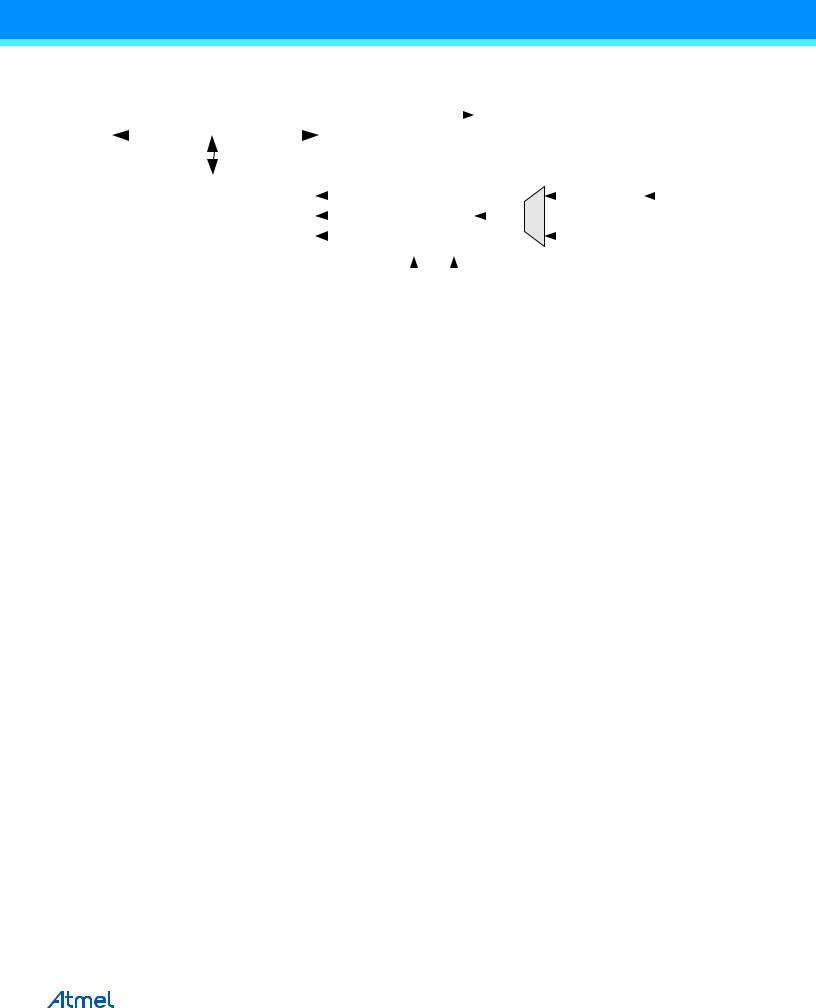
Figure 16-2. Counter Unit Block Diagram
|
|
|
|
|
|
|
|
|
|
|
|
TOVn |
|
|
|
|
|
|
|
||||
|
|
DATA BUS |
|
|
|
|
|
|
|
|
|
(Int.Req.) |
|
|
|
|
|
|
|
||||
|
|
|
|
|
|
|
|
|
|
|
|
|
|
|
|
|
|
|
|
|
|
|
|
|
|
|
|
|
|
|
|
|
|
|
|
|
|
|
|
|
Clock Select |
|
|
||||
|
|
|
|
|
|
count |
|
|
|
|
|
|
|
|
|
|
|
|
|
|
|
|
|
|
|
|
|
|
|
|
|
|
|
|
|
|
|
|
|
Edge |
|
|
|
Tn |
|||
|
|
TCNTn |
|
|
|
clear |
Control Logic |
clkTn |
|
|
|
Detector |
|
|
|
|
|||||||
|
|
|
|
|
|
|
|
|
|
|
|
||||||||||||
|
|
|
|
|
direction |
|
|
|
|
|
|
|
|
|
|
|
|
||||||
|
|
|
|
|
|
|
|
|
|
|
|
|
|
|
|
|
|
|
|
|
|
|
|
|
|
|
|
|
|
|
|
|
|
|
|
|
|
|
|
|
|
|
|
|
|||
|
|
|
|
|
|
|
|
|
|
|
|
|
|
|
|
|
|
|
|
|
|
|
|
|
|
|
|
|
|
|
|
|
|
|
|
|
|
|
|
|
( From Prescaler ) |
|
|
|
|||
|
|
|
|
|
|
|
|
|
|
|
|
|
|
|
|
|
|
|
|||||
|
|
|
|
|
|
|
|
|
|
|
|
|
|
|
|
|
|
|
|
|
|
||
|
|
|
|
|
|
|
|
|
|
|
|
|
|
|
|
|
|
|
|
|
|
|
|
|
|
|
|
|
|
bottom |
|
top |
|
|
|
|
|
|
|
||||||||
|
|
|
|
|
|
|
|
|
|
|
|
|
|
|
|
|
|
||||||
Signal description (internal signals): |
|
|
|
|
|
|
|
|
|
|
|
|
|
|
|||||||||
|
|
count |
Increment or decrement TCNT0 by 1. |
|
|
|
|
|
|
|
|||||||||||||
|
|
direction |
Select between increment and decrement. |
|
|
|
|
|
|
|
|||||||||||||
|
|
clear |
Clear TCNT0 (set all bits to zero). |
|
|
|
|
|
|
|
|||||||||||||
|
|
clkTn |
Timer/Counter clock, referred to as clkT0 in the following. |
|
|
||||||||||||||||||
|
|
top |
Signalize that TCNT0 has reached maximum value. |
|
|
||||||||||||||||||
|
|
bottom |
Signalize that TCNT0 has reached minimum value (zero). |
|
|
Depending of the mode of operation used, the counter is cleared, incremented, or decremented at each timer clock (clkT0). clkT0 can be generated from an external or internal clock source, selected by the Clock Select bits (CS02:0). When no clock source is selected (CS02:0 = 0) the timer is stopped. However, the TCNT0 value can be accessed by the CPU, regardless of whether clkT0 is present or not. A CPU write overrides (has priority over) all counter clear or count operations.
The counting sequence is determined by the setting of the WGM01 and WGM00 bits located in the Timer/Counter Control Register (TCCR0A) and the WGM02 bit located in the Timer/Counter Control Register B (TCCR0B). There are close connections between how the counter behaves (counts) and how waveforms are generated on the Output Compare outputs OC0A and OC0B. For more details about advanced counting sequences and waveform generation, see “Modes of Operation” on page 120.
The Timer/Counter Overflow Flag (TOV0) is set according to the mode of operation selected by the WGM02:0 bits. TOV0 can be used for generating a CPU interrupt.
16.5Output Compare Unit
The 8-bit comparator continuously compares TCNT0 with the Output Compare Registers (OCR0A and OCR0B). Whenever TCNT0 equals OCR0A or OCR0B, the comparator signals a match. A match will set the Output Compare Flag (OCF0A or OCF0B) at the next timer clock cycle. If the corresponding interrupt is enabled, the Output Compare Flag generates an Output Compare interrupt. The Output Compare Flag is automatically cleared when the interrupt is executed. Alternatively, the flag can be cleared by software by writing a logical one to its I/O bit location. The Waveform Generator uses the match signal to generate an output according to operating mode set by the WGM02:0 bits and Compare Output mode (COM0x1:0) bits. The maximum and bottom signals are used by the Waveform Generator for handling the special cases of the extreme values in some modes of operation (“Modes of Operation” on page 120).
Figure 16-3 on page 118 shows a block diagram of the Output Compare unit.
ATmega640/V-1280/V-1281/V-2560/V-2561/V [DATASHEET] |
117 |
2549Q–AVR–02/2014

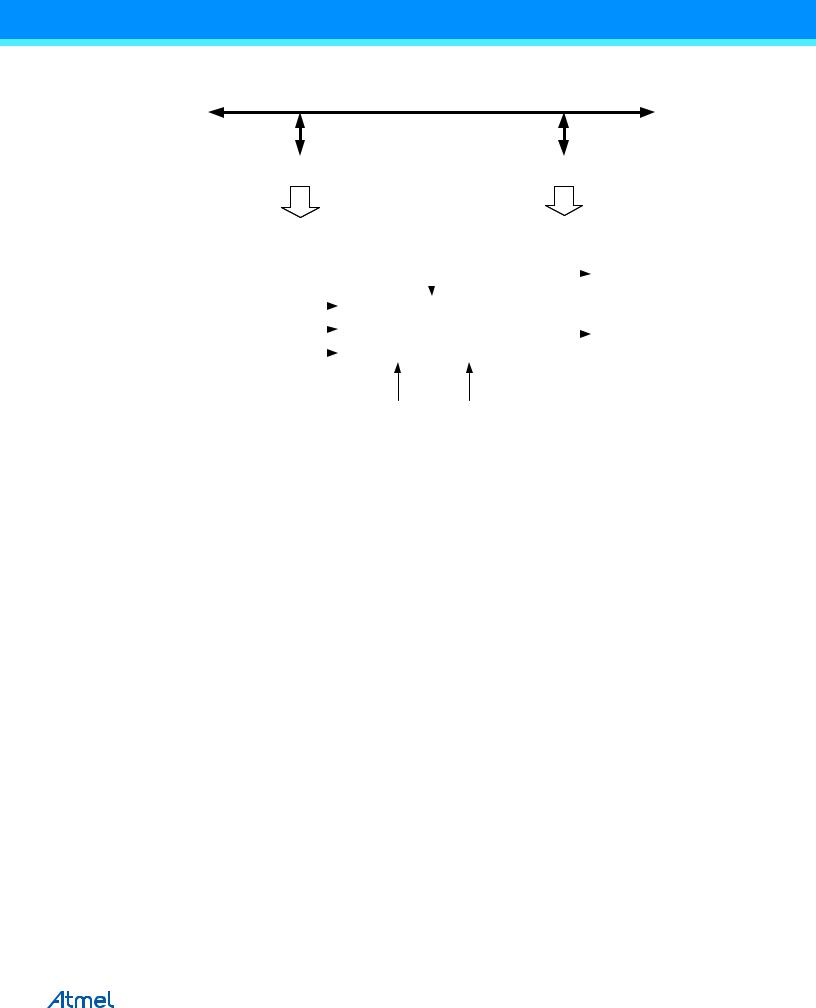
Figure 16-3. Output Compare Unit, Block Diagram
DATA BUS
|
OCRnx |
|
|
|
|
|
TCNTn |
|||
|
|
|
|
|
|
|
|
|
|
|
|
|
|
|
|
|
|
|
|
|
|
|
|
|
= (8-bit Comparator ) |
|
|
|
|
|||
|
|
|
|
|
|
|
OCFnx (Int.Req.) |
|||
top |
|
|
|
|
|
|
|
|
|
|
|
|
|
|
|
|
|
|
|
||
|
|
|
|
|
|
|
|
|
||
|
|
|
|
|
|
|
|
|
||
bottom |
|
|
Waveform Generator |
|
|
|
|
|||
|
|
|
OCnx |
|
||||||
FOCn |
|
|
|
|
||||||
|
|
|
|
|
|
|
|
|||
|
|
|
|
|
|
|
|
|
||
|
|
|
|
|
|
|
|
|
|
|
WGMn1:0 COMnX1:0
The OCR0x Registers are double buffered when using any of the Pulse Width Modulation (PWM) modes. For the normal and Clear Timer on Compare (CTC) modes of operation, the double buffering is disabled. The double buffering synchronizes the update of the OCR0x Compare Registers to either top or bottom of the counting sequence. The synchronization prevents the occurrence of odd-length, non-symmetrical PWM pulses, thereby making the output glitch-free.
The OCR0x Register access may seem complex, but this is not case. When the double buffering is enabled, the CPU has access to the OCR0x Buffer Register, and if double buffering is disabled the CPU will access the OCR0x directly.
16.5.1Force Output Compare
In non-PWM waveform generation modes, the match output of the comparator can be forced by writing a one to the Force Output Compare (FOC0x) bit. Forcing Compare Match will not set the OCF0x Flag or reload/clear the timer, but the OC0x pin will be updated as if a real Compare Match had occurred (the COM0x1:0 bits settings define whether the OC0x pin is set, cleared or toggled).
16.5.2Compare Match Blocking by TCNT0 Write
All CPU write operations to the TCNT0 Register will block any Compare Match that occur in the next timer clock cycle, even when the timer is stopped. This feature allows OCR0x to be initialized to the same value as TCNT0 without triggering an interrupt when the Timer/Counter clock is enabled.
16.5.3Using the Output Compare Unit
Since writing TCNT0 in any mode of operation will block all Compare Matches for one timer clock cycle, there are risks involved when changing TCNT0 when using the Output Compare Unit, independently of whether the Timer/Counter is running or not. If the value written to TCNT0 equals the OCR0x value, the Compare Match will be missed, resulting in incorrect waveform generation. Similarly, do not write the TCNT0 value equal to BOTTOM when the counter is down-counting.
ATmega640/V-1280/V-1281/V-2560/V-2561/V [DATASHEET] |
118 |
2549Q–AVR–02/2014