

- •1. Pin Configurations
- •2. Overview
- •2.1 Block Diagram
- •2.2 Comparison Between ATmega1281/2561 and ATmega640/1280/2560
- •2.3 Pin Descriptions
- •2.3.3 Port A (PA7..PA0)
- •2.3.4 Port B (PB7..PB0)
- •2.3.5 Port C (PC7..PC0)
- •2.3.6 Port D (PD7..PD0)
- •2.3.7 Port E (PE7..PE0)
- •2.3.8 Port F (PF7..PF0)
- •2.3.9 Port G (PG5..PG0)
- •2.3.10 Port H (PH7..PH0)
- •2.3.11 Port J (PJ7..PJ0)
- •2.3.12 Port K (PK7..PK0)
- •2.3.13 Port L (PL7..PL0)
- •2.3.14 RESET
- •2.3.15 XTAL1
- •2.3.16 XTAL2
- •2.3.17 AVCC
- •2.3.18 AREF
- •3. Resources
- •4. About Code Examples
- •5. Data Retention
- •6. Capacitive touch sensing
- •7. AVR CPU Core
- •7.1 Introduction
- •7.2 Architectural Overview
- •7.3 ALU – Arithmetic Logic Unit
- •7.4 Status Register
- •7.4.1 SREG – AVR Status Register
- •7.5 General Purpose Register File
- •7.6 Stack Pointer
- •7.6.2 EIND – Extended Indirect Register
- •7.7 Instruction Execution Timing
- •7.8 Reset and Interrupt Handling
- •7.8.1 Interrupt Response Time
- •8. AVR Memories
- •8.2 SRAM Data Memory
- •8.2.1 Data Memory Access Times
- •8.3 EEPROM Data Memory
- •8.3.1 EEPROM Read/Write Access
- •8.3.2 Preventing EEPROM Corruption
- •8.4 I/O Memory
- •8.4.1 General Purpose I/O Registers
- •9. External Memory Interface
- •9.1 Overview
- •9.1.1 Using the External Memory Interface
- •9.1.2 Address Latch Requirements
- •9.1.4 Timing
- •9.1.5 Using all Locations of External Memory Smaller than 64Kbytes
- •9.1.6 Using all 64Kbytes Locations of External Memory
- •9.2 Register Description
- •9.2.1 EEPROM registers
- •9.3 General Purpose registers
- •9.3.1 GPIOR2 – General Purpose I/O Register 2
- •9.3.2 GPIOR1 – General Purpose I/O Register 1
- •9.3.3 GPIOR0 – General Purpose I/O Register 0
- •9.4 External Memory registers
- •9.4.1 XMCRA – External Memory Control Register A
- •9.4.2 XMCRB – External Memory Control Register B
- •10. System Clock and Clock Options
- •10.1 Overview
- •10.2 Clock Systems and their Distribution
- •10.3 Clock Sources
- •10.3.1 Default Clock Source
- •10.4 Low Power Crystal Oscillator
- •10.5 Full Swing Crystal Oscillator
- •10.6 Low Frequency Crystal Oscillator
- •10.7 Calibrated Internal RC Oscillator
- •10.8 128kHz Internal Oscillator
- •10.9 External Clock
- •10.10 Clock Output Buffer
- •10.11 Timer/Counter Oscillator
- •10.12 System Clock Prescaler
- •10.13 Register Description
- •10.13.1 OSCCAL – Oscillator Calibration Register
- •10.13.2 CLKPR – Clock Prescale Register
- •11. Power Management and Sleep Modes
- •11.1 Sleep Modes
- •11.2 Idle Mode
- •11.3 ADC Noise Reduction Mode
- •11.6 Standby Mode
- •11.7 Extended Standby Mode
- •11.8 Power Reduction Register
- •11.9 Minimizing Power Consumption
- •11.9.1 Analog to Digital Converter
- •11.9.2 Analog Comparator
- •11.9.4 Internal Voltage Reference
- •11.9.5 Watchdog Timer
- •11.9.6 Port Pins
- •11.10 Register Description
- •11.10.1 SMCR – Sleep Mode Control Register
- •11.10.2 PRR0 – Power Reduction Register 0
- •11.10.3 PRR1 – Power Reduction Register 1
- •12. System Control and Reset
- •12.1 Resetting the AVR
- •12.2 Reset Sources
- •12.2.1 Power-on Reset
- •12.2.2 External Reset
- •12.2.4 Watchdog Reset
- •12.3 Internal Voltage Reference
- •12.4 Watchdog Timer
- •12.4.1 Features
- •12.4.2 Overview
- •12.5 Register Description
- •12.5.1 MCUSR – MCU Status Register
- •12.5.2 WDTCSR – Watchdog Timer Control Register
- •13. I/O-Ports
- •13.1 Introduction
- •13.2 Ports as General Digital I/O
- •13.2.1 Configuring the Pin
- •13.2.2 Toggling the Pin
- •13.2.3 Switching Between Input and Output
- •13.2.4 Reading the Pin Value
- •13.2.5 Digital Input Enable and Sleep Modes
- •13.2.6 Unconnected Pins
- •13.3 Alternate Port Functions
- •13.3.1 Alternate Functions of Port A
- •13.3.2 Alternate Functions of Port B
- •13.3.3 Alternate Functions of Port C
- •13.3.4 Alternate Functions of Port D
- •13.3.5 Alternate Functions of Port E
- •13.3.6 Alternate Functions of Port F
- •13.3.7 Alternate Functions of Port G
- •13.3.8 Alternate Functions of Port H
- •13.3.9 Alternate Functions of Port J
- •13.3.10 Alternate Functions of Port K
- •13.3.11 Alternate Functions of Port L
- •13.4.1 MCUCR – MCU Control Register
- •13.4.2 PORTA – Port A Data Register
- •13.4.3 DDRA – Port A Data Direction Register
- •13.4.4 PINA – Port A Input Pins Address
- •13.4.5 PORTB – Port B Data Register
- •13.4.6 DDRB – Port B Data Direction Register
- •13.4.7 PINB – Port B Input Pins Address
- •13.4.8 PORTC – Port C Data Register
- •13.4.9 DDRC – Port C Data Direction Register
- •13.4.10 PINC– Port C Input Pins Address
- •13.4.11 PORTD – Port D Data Register
- •13.4.12 DDRD – Port D Data Direction Register
- •13.4.13 PIND – Port D Input Pins Address
- •13.4.14 PORTE – Port E Data Register
- •13.4.15 DDRE – Port E Data Direction Register
- •13.4.16 PINE – Port E Input Pins Address
- •13.4.17 PORTF – Port F Data Register
- •13.4.18 DDRF – Port F Data Direction Register
- •13.4.19 PINF – Port F Input Pins Address
- •13.4.20 PORTG – Port G Data Register
- •13.4.21 DDRG – Port G Data Direction Register
- •13.4.22 PING – Port G Input Pins Address
- •13.4.23 PORTH – Port H Data Register
- •13.4.24 DDRH – Port H Data Direction Register
- •13.4.25 PINH – Port H Input Pins Address
- •13.4.26 PORTJ – Port J Data Register
- •13.4.27 DDRJ – Port J Data Direction Register
- •13.4.28 PINJ – Port J Input Pins Address
- •13.4.29 PORTK – Port K Data Register
- •13.4.30 DDRK – Port K Data Direction Register
- •13.4.31 PINK – Port K Input Pins Address
- •13.4.32 PORTL – Port L Data Register
- •13.4.33 DDRL – Port L Data Direction Register
- •13.4.34 PINL – Port L Input Pins Address
- •14. Interrupts
- •14.1 Interrupt Vectors in ATmega640/1280/1281/2560/2561
- •14.2 Reset and Interrupt Vector placement
- •14.3 Moving Interrupts Between Application and Boot Section
- •14.4 Register Description
- •14.4.1 MCUCR – MCU Control Register
- •15. External Interrupts
- •15.1 Pin Change Interrupt Timing
- •15.2 Register Description
- •15.2.1 EICRA – External Interrupt Control Register A
- •15.2.2 EICRB – External Interrupt Control Register B
- •15.2.3 EIMSK – External Interrupt Mask Register
- •15.2.4 EIFR – External Interrupt Flag Register
- •15.2.5 PCICR – Pin Change Interrupt Control Register
- •15.2.6 PCIFR – Pin Change Interrupt Flag Register
- •15.2.7 PCMSK2 – Pin Change Mask Register 2
- •15.2.8 PCMSK1 – Pin Change Mask Register 1
- •15.2.9 PCMSK0 – Pin Change Mask Register 0
- •16. 8-bit Timer/Counter0 with PWM
- •16.1 Features
- •16.2 Overview
- •16.2.1 Registers
- •16.2.2 Definitions
- •16.3 Timer/Counter Clock Sources
- •16.4 Counter Unit
- •16.5 Output Compare Unit
- •16.5.1 Force Output Compare
- •16.5.2 Compare Match Blocking by TCNT0 Write
- •16.5.3 Using the Output Compare Unit
- •16.6 Compare Match Output Unit
- •16.6.1 Compare Output Mode and Waveform Generation
- •16.7 Modes of Operation
- •16.7.1 Normal Mode
- •16.7.2 Clear Timer on Compare Match (CTC) Mode
- •16.7.3 Fast PWM Mode
- •16.7.4 Phase Correct PWM Mode
- •16.8 Timer/Counter Timing Diagrams
- •16.9 Register Description
- •16.9.1 TCCR0A – Timer/Counter Control Register A
- •16.9.2 TCCR0B – Timer/Counter Control Register B
- •16.9.3 TCNT0 – Timer/Counter Register
- •16.9.4 OCR0A – Output Compare Register A
- •16.9.5 OCR0B – Output Compare Register B
- •16.9.6 TIMSK0 – Timer/Counter Interrupt Mask Register
- •16.9.7 TIFR0 – Timer/Counter 0 Interrupt Flag Register
- •17. 16-bit Timer/Counter (Timer/Counter 1, 3, 4, and 5)
- •17.1 Features
- •17.2 Overview
- •17.2.1 Registers
- •17.2.2 Definitions
- •17.3.1 Reusing the Temporary High Byte Register
- •17.4 Timer/Counter Clock Sources
- •17.5 Counter Unit
- •17.6 Input Capture Unit
- •17.6.1 Input Capture Trigger Source
- •17.6.2 Noise Canceler
- •17.6.3 Using the Input Capture Unit
- •17.7 Output Compare Units
- •17.7.1 Force Output Compare
- •17.7.2 Compare Match Blocking by TCNTn Write
- •17.7.3 Using the Output Compare Unit
- •17.8 Compare Match Output Unit
- •17.8.1 Compare Output Mode and Waveform Generation
- •17.9 Modes of Operation
- •17.9.1 Normal Mode
- •17.9.2 Clear Timer on Compare Match (CTC) Mode
- •17.9.3 Fast PWM Mode
- •17.9.4 Phase Correct PWM Mode
- •17.9.5 Phase and Frequency Correct PWM Mode
- •17.10 Timer/Counter Timing Diagrams
- •17.11 Register Description
- •17.11.1 TCCR1A – Timer/Counter 1 Control Register A
- •17.11.2 TCCR3A – Timer/Counter 3 Control Register A
- •17.11.3 TCCR4A – Timer/Counter 4 Control Register A
- •17.11.4 TCCR5A – Timer/Counter 5 Control Register A
- •17.11.5 TCCR1B – Timer/Counter 1 Control Register B
- •17.11.6 TCCR3B – Timer/Counter 3 Control Register B
- •17.11.7 TCCR4B – Timer/Counter 4 Control Register B
- •17.11.8 TCCR5B – Timer/Counter 5 Control Register B
- •17.11.9 TCCR1C – Timer/Counter 1 Control Register C
- •17.11.10 TCCR3C – Timer/Counter 3 Control Register C
- •17.11.11 TCCR4C – Timer/Counter 4 Control Register C
- •17.11.12 TCCR5C – Timer/Counter 5 Control Register C
- •17.11.13 TCNT1H and TCNT1L – Timer/Counter 1
- •17.11.14 TCNT3H and TCNT3L – Timer/Counter 3
- •17.11.15 TCNT4H and TCNT4L –Timer/Counter 4
- •17.11.16 TCNT5H and TCNT5L –Timer/Counter 5
- •17.11.17 OCR1AH and OCR1AL – Output Compare Register 1 A
- •17.11.18 OCR1BH and OCR1BL – Output Compare Register 1 B
- •17.11.19 OCR1CH and OCR1CL – Output Compare Register 1 C
- •17.11.20 OCR3AH and OCR3AL – Output Compare Register 3 A
- •17.11.21 OCR3BH and OCR3BL – Output Compare Register 3 B
- •17.11.22 OCR3CH and OCR3CL – Output Compare Register 3 C
- •17.11.23 OCR4AH and OCR4AL – Output Compare Register 4 A
- •17.11.24 OCR4BH and OCR4BL – Output Compare Register 4 B
- •17.11.25 OCR4CH and OCR4CL –Output Compare Register 4 C
- •17.11.26 OCR5AH and OCR5AL – Output Compare Register 5 A
- •17.11.27 OCR5BH and OCR5BL – Output Compare Register 5 B
- •17.11.28 OCR5CH and OCR5CL –Output Compare Register 5 C
- •17.11.29 ICR1H and ICR1L – Input Capture Register 1
- •17.11.30 ICR3H and ICR3L – Input Capture Register 3
- •17.11.31 ICR4H and ICR4L – Input Capture Register 4
- •17.11.32 ICR5H and ICR5L – Input Capture Register 5
- •17.11.33 TIMSK1 – Timer/Counter 1 Interrupt Mask Register
- •17.11.34 TIMSK3 – Timer/Counter 3 Interrupt Mask Register
- •17.11.35 TIMSK4 – Timer/Counter 4 Interrupt Mask Register
- •17.11.36 TIMSK5 – Timer/Counter 5 Interrupt Mask Register
- •17.11.37 TIFR1 – Timer/Counter1 Interrupt Flag Register
- •17.11.38 TIFR3 – Timer/Counter3 Interrupt Flag Register
- •17.11.39 TIFR4 – Timer/Counter4 Interrupt Flag Register
- •17.11.40 TIFR5 – Timer/Counter5 Interrupt Flag Register
- •18. Timer/Counter 0, 1, 3, 4, and 5 Prescaler
- •18.1 Internal Clock Source
- •18.2 Prescaler Reset
- •18.3 External Clock Source
- •18.4 Register Description
- •18.4.1 GTCCR – General Timer/Counter Control Register
- •19. Output Compare Modulator (OCM1C0A)
- •19.1 Overview
- •19.2 Description
- •19.2.1 Timing example
- •20. 8-bit Timer/Counter2 with PWM and Asynchronous Operation
- •20.1 Overview
- •20.1.1 Registers
- •20.1.2 Definitions
- •20.2 Timer/Counter Clock Sources
- •20.3 Counter Unit
- •20.4 Modes of Operation
- •20.4.1 Normal Mode
- •20.4.2 Clear Timer on Compare Match (CTC) Mode
- •20.4.3 Fast PWM Mode
- •20.4.4 Phase Correct PWM Mode
- •20.5 Output Compare Unit
- •20.5.1 Force Output Compare
- •20.5.2 Compare Match Blocking by TCNT2 Write
- •20.5.3 Using the Output Compare Unit
- •20.6 Compare Match Output Unit
- •20.6.1 Compare Output Mode and Waveform Generation
- •20.7 Timer/Counter Timing Diagrams
- •20.8 Asynchronous Operation of Timer/Counter2
- •20.9 Timer/Counter Prescaler
- •20.10 Register Description
- •20.10.2 TCCR2B – Timer/Counter Control Register B
- •20.10.3 TCNT2 – Timer/Counter Register
- •20.10.4 OCR2A – Output Compare Register A
- •20.10.5 OCR2B – Output Compare Register B
- •20.10.6 ASSR – Asynchronous Status Register
- •20.10.7 TIMSK2 – Timer/Counter2 Interrupt Mask Register
- •20.10.8 TIFR2 – Timer/Counter2 Interrupt Flag Register
- •20.10.9 GTCCR – General Timer/Counter Control Register
- •21. SPI – Serial Peripheral Interface
- •21.1 SS Pin Functionality
- •21.1.1 Slave Mode
- •21.1.2 Master Mode
- •21.1.3 Data Modes
- •21.2 Register Description
- •21.2.1 SPCR – SPI Control Register
- •21.2.2 SPSR – SPI Status Register
- •21.2.3 SPDR – SPI Data Register
- •22. USART
- •22.1 Features
- •22.2 Overview
- •22.3 Clock Generation
- •22.3.1 Internal Clock Generation – The Baud Rate Generator
- •22.3.2 Double Speed Operation (U2Xn)
- •22.3.3 External Clock
- •22.3.4 Synchronous Clock Operation
- •22.4 Frame Formats
- •22.4.1 Parity Bit Calculation
- •22.5 USART Initialization
- •22.6 Data Transmission – The USART Transmitter
- •22.6.1 Sending Frames with 5 to 8 Data Bit
- •22.6.2 Sending Frames with 9 Data Bit
- •22.6.3 Transmitter Flags and Interrupts
- •22.6.4 Parity Generator
- •22.6.5 Disabling the Transmitter
- •22.7 Data Reception – The USART Receiver
- •22.7.1 Receiving Frames with 5 to 8 Data Bits
- •22.7.2 Receiving Frames with 9 Data Bits
- •22.7.3 Receive Compete Flag and Interrupt
- •22.7.4 Receiver Error Flags
- •22.7.5 Parity Checker
- •22.7.6 Disabling the Receiver
- •22.7.7 Flushing the Receive Buffer
- •22.8 Asynchronous Data Reception
- •22.8.1 Asynchronous Clock Recovery
- •22.8.2 Asynchronous Data Recovery
- •22.8.3 Asynchronous Operational Range
- •22.9.1 Using MPCMn
- •22.10 Register Description
- •22.10.1 UDRn – USART I/O Data Register n
- •22.10.2 UCSRnA – USART Control and Status Register A
- •22.10.3 UCSRnB – USART Control and Status Register n B
- •22.10.4 UCSRnC – USART Control and Status Register n C
- •22.10.5 UBRRnL and UBRRnH – USART Baud Rate Registers
- •22.11 Examples of Baud Rate Setting
- •23. USART in SPI Mode
- •23.1 Overview
- •23.2 USART MSPIM vs. SPI
- •23.2.1 Clock Generation
- •23.3 SPI Data Modes and Timing
- •23.4 Frame Formats
- •23.4.1 USART MSPIM Initialization
- •23.5 Data Transfer
- •23.5.1 Transmitter and Receiver Flags and Interrupts
- •23.5.2 Disabling the Transmitter or Receiver
- •23.6 USART MSPIM Register Description
- •23.6.1 UDRn – USART MSPIM I/O Data Register
- •23.6.2 UCSRnA – USART MSPIM Control and Status Register n A
- •23.6.3 UCSRnB – USART MSPIM Control and Status Register n B
- •23.6.4 UCSRnC – USART MSPIM Control and Status Register n C
- •23.6.5 UBRRnL and UBRRnH – USART MSPIM Baud Rate Registers
- •24. 2-wire Serial Interface
- •24.1 Features
- •24.2.1 TWI Terminology
- •24.2.2 Electrical Interconnection
- •24.3 Data Transfer and Frame Format
- •24.3.1 Transferring Bits
- •24.3.2 START and STOP Conditions
- •24.3.3 Address Packet Format
- •24.3.4 Data Packet Format
- •24.3.5 Combining Address and Data Packets into a Transmission
- •24.5 Overview of the TWI Module
- •24.5.1 SCL and SDA Pins
- •24.5.2 Bit Rate Generator Unit
- •24.5.3 Bus Interface Unit
- •24.5.4 Address Match Unit
- •24.5.5 Control Unit
- •24.6 Using the TWI
- •24.7 Transmission Modes
- •24.7.1 Master Transmitter Mode
- •24.7.2 Master Receiver Mode
- •24.7.3 Slave Receiver Mode
- •24.7.4 Slave Transmitter Mode
- •24.7.5 Miscellaneous States
- •24.7.6 Combining Several TWI Modes
- •24.9 Register Description
- •24.9.1 TWBR – TWI Bit Rate Register
- •24.9.2 TWCR – TWI Control Register
- •24.9.3 TWSR – TWI Status Register
- •24.9.4 TWDR – TWI Data Register
- •24.9.5 TWAR – TWI (Slave) Address Register
- •24.9.6 TWAMR – TWI (Slave) Address Mask Register
- •25. AC – Analog Comparator
- •25.1 Analog Comparator Multiplexed Input
- •25.2 Register Description
- •25.2.1 ADCSRB – ADC Control and Status Register B
- •25.2.2 ACSR – Analog Comparator Control and Status Register
- •25.2.3 DIDR1 – Digital Input Disable Register 1
- •26. ADC – Analog to Digital Converter
- •26.1 Features
- •26.2 Operation
- •26.3 Starting a Conversion
- •26.4 Prescaling and Conversion Timing
- •26.4.1 Differential Channels
- •26.5 Changing Channel or Reference Selection
- •26.5.1 ADC Input Channels
- •26.5.2 ADC Voltage Reference
- •26.6 ADC Noise Canceler
- •26.6.1 Analog Input Circuitry
- •26.6.2 Analog Noise Canceling Techniques
- •26.6.3 Offset Compensation Schemes
- •26.6.4 ADC Accuracy Definitions
- •26.7 ADC Conversion Result
- •26.8 Register Description
- •26.8.1 ADMUX – ADC Multiplexer Selection Register
- •26.8.2 ADCSRB – ADC Control and Status Register B
- •26.8.3 ADCSRA – ADC Control and Status Register A
- •26.8.4 ADCL and ADCH – The ADC Data Register
- •26.8.5 ADCSRB – ADC Control and Status Register B
- •26.8.6 DIDR0 – Digital Input Disable Register 0
- •26.8.7 DIDR2 – Digital Input Disable Register 2
- •27. JTAG Interface and On-chip Debug System
- •27.1 Features
- •27.2 Overview
- •27.3 TAP - Test Access Port
- •27.3.1 TAP Controller
- •27.6.1 PRIVATE0; 0x8
- •27.6.2 PRIVATE1; 0x9
- •27.6.3 PRIVATE2; 0xA
- •27.6.4 PRIVATE3; 0xB
- •27.7 Using the JTAG Programming Capabilities
- •27.8 Bibliography
- •28. IEEE 1149.1 (JTAG) Boundary-scan
- •28.1 Features
- •28.2 System Overview
- •28.3 Data Registers
- •28.3.1 Bypass Register
- •28.3.2 Device Identification Register
- •28.3.3 Reset Register
- •28.4.1 EXTEST; 0x0
- •28.4.2 IDCODE; 0x1
- •28.4.3 SAMPLE_PRELOAD; 0x2
- •28.4.4 AVR_RESET; 0xC
- •28.4.5 BYPASS; 0xF
- •28.5.1 Scanning the Digital Port Pins
- •28.5.2 Scanning the RESET Pin
- •28.6.1 MCUCR – MCU Control Register
- •28.6.2 MCUSR – MCU Status Register
- •29. Boot Loader Support – Read-While-Write Self-Programming
- •29.1 Features
- •29.2 Application and Boot Loader Flash Sections
- •29.2.1 Application Section
- •29.2.2 BLS – Boot Loader Section
- •29.4 Boot Loader Lock Bits
- •29.4.1 Entering the Boot Loader Program
- •29.6.1 Performing Page Erase by SPM
- •29.6.2 Filling the Temporary Buffer (Page Loading)
- •29.6.3 Performing a Page Write
- •29.6.4 Using the SPM Interrupt
- •29.6.5 Consideration While Updating BLS
- •29.6.7 Setting the Boot Loader Lock Bits by SPM
- •29.6.8 EEPROM Write Prevents Writing to SPMCSR
- •29.6.9 Reading the Fuse and Lock Bits from Software
- •29.6.10 Reading the Signature Row from Software
- •29.6.11 Preventing Flash Corruption
- •29.6.12 Programming Time for Flash when Using SPM
- •29.6.13 Simple Assembly Code Example for a Boot Loader
- •29.6.14 ATmega640 Boot Loader Parameters
- •29.6.15 ATmega1280/1281 Boot Loader Parameters
- •29.6.16 ATmega2560/2561 Boot Loader Parameters
- •29.7 Register Description
- •29.7.1 SPMCSR – Store Program Memory Control and Status Register
- •30. Memory Programming
- •30.1 Program And Data Memory Lock Bits
- •30.2 Fuse Bits
- •30.2.1 Latching of Fuses
- •30.3 Signature Bytes
- •30.4 Calibration Byte
- •30.5 Page Size
- •30.6 Parallel Programming Parameters, Pin Mapping, and Commands
- •30.6.1 Signal Names
- •30.7 Parallel Programming
- •30.7.1 Enter Programming Mode
- •30.7.2 Considerations for Efficient Programming
- •30.7.3 Chip Erase
- •30.7.4 Programming the Flash
- •30.7.5 Programming the EEPROM
- •30.7.6 Reading the Flash
- •30.7.7 Reading the EEPROM
- •30.7.8 Programming the Fuse Low Bits
- •30.7.9 Programming the Fuse High Bits
- •30.7.10 Programming the Extended Fuse Bits
- •30.7.11 Programming the Lock Bits
- •30.7.12 Reading the Fuse and Lock Bits
- •30.7.13 Reading the Signature Bytes
- •30.7.14 Reading the Calibration Byte
- •30.7.15 Parallel Programming Characteristics
- •30.8 Serial Downloading
- •30.8.1 Serial Programming Pin Mapping
- •30.8.2 Serial Programming Algorithm
- •30.8.3 Serial Programming Instruction set
- •30.8.4 Serial Programming Characteristics
- •30.9 Programming via the JTAG Interface
- •30.9.1 Programming Specific JTAG Instructions
- •30.9.2 AVR_RESET (0xC)
- •30.9.3 PROG_ENABLE (0x4)
- •30.9.4 PROG_COMMANDS (0x5)
- •30.9.5 PROG_PAGELOAD (0x6)
- •30.9.6 PROG_PAGEREAD (0x7)
- •30.9.7 Data Registers
- •30.9.8 Reset Register
- •30.9.9 Programming Enable Register
- •30.9.10 Programming Command Register
- •30.9.11 Flash Data Byte Register
- •30.9.12 Programming Algorithm
- •30.9.13 Entering Programming Mode
- •30.9.14 Leaving Programming Mode
- •30.9.15 Performing Chip Erase
- •30.9.16 Programming the Flash
- •30.9.17 Reading the Flash
- •30.9.18 Programming the EEPROM
- •30.9.19 Reading the EEPROM
- •30.9.20 Programming the Fuses
- •30.9.21 Programming the Lock Bits
- •30.9.22 Reading the Fuses and Lock Bits
- •30.9.23 Reading the Signature Bytes
- •30.9.24 Reading the Calibration Byte
- •31. Electrical Characteristics
- •31.1 DC Characteristics
- •31.2 Speed Grades
- •31.3 Clock Characteristics
- •31.3.1 Calibrated Internal RC Oscillator Accuracy
- •31.3.2 External Clock Drive Waveforms
- •31.4 External Clock Drive
- •31.5 System and Reset Characteristics
- •31.7 SPI Timing Characteristics
- •31.8 ADC Characteristics – Preliminary Data
- •31.9 External Data Memory Timing
- •32. Typical Characteristics
- •32.1 Active Supply Current
- •32.2 Idle Supply Current
- •32.2.1 Supply Current of IO modules
- •32.5 Standby Supply Current
- •32.7 Pin Driver Strength
- •32.8 Pin Threshold and Hysteresis
- •32.9 BOD Threshold and Analog Comparator Offset
- •32.10 Internal Oscillator Speed
- •32.11 Current Consumption of Peripheral Units
- •32.12 Current Consumption in Reset and Reset Pulsewidth
- •33. Register Summary
- •34. Instruction Set Summary
- •35. Ordering Information
- •35.1 ATmega640
- •35.2 ATmega1280
- •35.3 ATmega1281
- •35.4 ATmega2560
- •35.5 ATmega2561
- •36. Packaging Information
- •37. Errata
- •37.1 ATmega640 rev. B
- •37.2 ATmega640 rev. A
- •37.3 ATmega1280 rev. B
- •37.4 ATmega1280 rev. A
- •37.5 ATmega1281 rev. B
- •37.6 ATmega1281 rev. A
- •37.7 ATmega2560 rev. F
- •37.8 ATmega2560 rev. E
- •37.9 ATmega2560 rev. D
- •37.10 ATmega2560 rev. C
- •37.11 ATmega2560 rev. B
- •37.12 ATmega2560 rev. A
- •37.13 ATmega2561 rev. F
- •37.14 ATmega2561 rev. E
- •37.15 ATmega2561 rev. D
- •37.16 ATmega2561 rev. C
- •37.17 ATmega2561 rev. B
- •37.18 ATmega2561 rev. A
- •38. Datasheet Revision History

Table 30-11. Pin Values Used to Enter Programming Mode
Pin |
Symbol |
Value |
|
|
|
PAGEL |
Prog_enable[3] |
0 |
|
|
|
XA1 |
Prog_enable[2] |
0 |
|
|
|
XA0 |
Prog_enable[1] |
0 |
|
|
|
BS1 |
Prog_enable[0] |
0 |
|
|
|
Table 30-12. XA1 and XA0 Enoding
XA1 |
XA0 |
Action when XTAL1 is Pulsed |
|
|
|
0 |
0 |
Load Flash or EEPROM Address (High or low address byte determined by BS2 and BS1) |
|
|
|
0 |
1 |
Load Data (High or Low data byte for Flash determined by BS1) |
|
|
|
1 |
0 |
Load Command |
|
|
|
1 |
1 |
No Action, Idle |
|
|
|
Table 30-13. Command Byte Bit Encoding
Command Byte |
Command Executed |
|
|
1000 0000 |
Chip Erase |
|
|
0100 0000 |
Write Fuse bits |
|
|
0010 0000 |
Write Lock bits |
|
|
0001 0000 |
Write Flash |
|
|
0001 0001 |
Write EEPROM |
|
|
0000 1000 |
Read Signature Bytes and Calibration byte |
|
|
0000 0100 |
Read Fuse and Lock bits |
|
|
0000 0010 |
Read Flash |
|
|
0000 0011 |
Read EEPROM |
|
|
30.7Parallel Programming
30.7.1Enter Programming Mode
The following algorithm puts the device in parallel programming mode:
1.Apply 4.5V - 5.5V between VCC and GND.
2.Set RESET to “0” and toggle XTAL1 at least six times.
3.Set the Prog_enable pins listed in Table 30-11 to “0000” and wait at least 100ns.
4.Apply 11.5V - 12.5V to RESET. Any activity on Prog_enable pins within 100ns after +12V has been applied to RESET, will cause the device to fail entering programming mode.
5.Wait at least 50µs before sending a new command.
ATmega640/V-1280/V-1281/V-2560/V-2561/V [DATASHEET] |
330 |
2549Q–AVR–02/2014
30.7.2Considerations for Efficient Programming
The loaded command and address are retained in the device during programming. For efficient programming, the following should be considered.
•The command needs only be loaded once when writing or reading multiple memory locations
•Skip writing the data value 0xFF, that is the contents of the entire EEPROM (unless the EESAVE Fuse is programmed) and Flash after a Chip Erase
•Address high byte needs only be loaded before programming or reading a new 256 word window in Flash or 256 byte EEPROM. This consideration also applies to Signature bytes reading
30.7.3Chip Erase
The Chip Erase will erase the Flash and EEPROM(1) memories plus Lock bits. The Lock bits are not reset until the program memory has been completely erased. The Fuse bits are not changed. A Chip Erase must be performed before the Flash and/or EEPROM are reprogrammed.
Note: 1. The EEPRPOM memory is preserved during Chip Erase if the EESAVE Fuse is programmed.
Load Command “Chip Erase”
1.Set XA1, XA0 to “10”. This enables command loading.
2.Set BS1 to “0”.
3.Set DATA to “1000 0000”. This is the command for Chip Erase.
4.Give XTAL1 a positive pulse. This loads the command.
5.Give WR a negative pulse. This starts the Chip Erase. RDY/BSY goes low.
6.Wait until RDY/BSY goes high before loading a new command.
30.7.4Programming the Flash
The Flash is organized in pages, see Table 30-7 on page 328. When programming the Flash, the program data is latched into a page buffer. This allows one page of program data to be programmed simultaneously. The following procedure describes how to program the entire Flash memory:
A. Load Command “Write Flash”
1.Set XA1, XA0 to “10”. This enables command loading.
2.Set BS1 to “0”.
3.Set DATA to “0001 0000”. This is the command for Write Flash.
4.Give XTAL1 a positive pulse. This loads the command.
B. Load Address Low byte (Address bits 7:0)
1.Set XA1, XA0 to “00”. This enables address loading.
2.Set BS2, BS1 to “00”. This selects the address low byte.
3.Set DATA = Address low byte (0x00 - 0xFF).
4.Give XTAL1 a positive pulse. This loads the address low byte. C. Load Data Low Byte
1.Set XA1, XA0 to “01”. This enables data loading.
2.Set DATA = Data low byte (0x00 - 0xFF).
3.Give XTAL1 a positive pulse. This loads the data byte.
ATmega640/V-1280/V-1281/V-2560/V-2561/V [DATASHEET] |
331 |
2549Q–AVR–02/2014

D. Load Data High Byte
1.Set BS1 to “1”. This selects high data byte.
2.Set XA1, XA0 to “01”. This enables data loading.
3.Set DATA = Data high byte (0x00 - 0xFF).
4.Give XTAL1 a positive pulse. This loads the data byte. E. Latch Data
1.Set BS1 to “1”. This selects high data byte.
2.Give PAGEL a positive pulse. This latches the data bytes. See Figure 30-3 on page 333 for signal waveforms.
F. Repeat B through E until the entire buffer is filled or until all data within the page is loaded
While the lower bits in the address are mapped to words within the page, the higher bits address the pages within the FLASH. This is illustrated in Figure 30-2 on page 333. Note that if less than eight bits are required to address words in the page (pagesize < 256), the most significant bit(s) in the address low byte are used to address the page when performing a Page Write.
G. Load Address High byte (Address bits15:8)
1.Set XA1, XA0 to “00”. This enables address loading.
2.Set BS2, BS1 to “01”. This selects the address high byte.
3.Set DATA = Address high byte (0x00 - 0xFF).
4.Give XTAL1 a positive pulse. This loads the address high byte. H. Load Address Extended High byte (Address bits 23:16)
1.Set XA1, XA0 to “00”. This enables address loading.
2.Set BS2, BS1 to “10”. This selects the address extended high byte.
3.Set DATA = Address extended high byte (0x00 - 0xFF).
4.Give XTAL1 a positive pulse. This loads the address high byte.
I. Program Page
1.Set BS2, BS1 to “00”.
2.Give WR a negative pulse. This starts programming of the entire page of data. RDY/BSY goes low.
3.Wait until RDY/BSY goes high (see Figure 30-3 on page 333 for signal waveforms).
J.Repeat B through I until the entire Flash is programmed or until all data has been programmed
K.End Page Programming
1.1. Set XA1, XA0 to “10”. This enables command loading.
2.Set DATA to “0000 0000”. This is the command for No Operation.
3.Give XTAL1 a positive pulse. This loads the command, and the internal write signals are reset.
ATmega640/V-1280/V-1281/V-2560/V-2561/V [DATASHEET] |
332 |
2549Q–AVR–02/2014
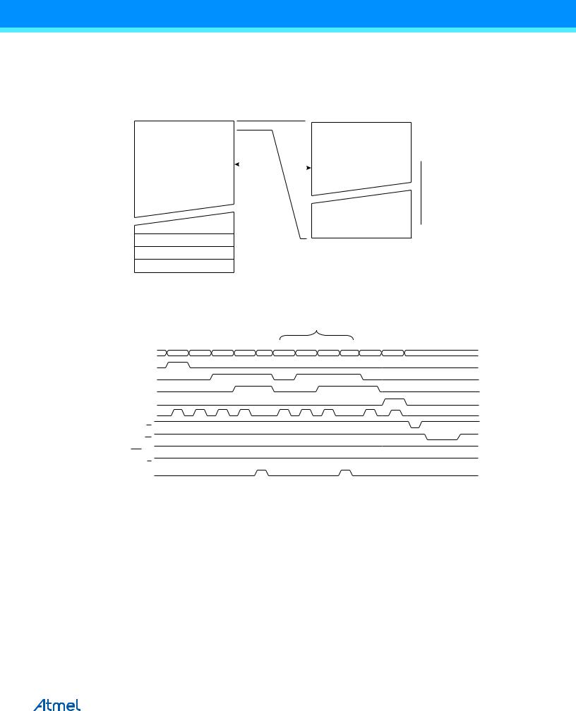
Figure 30-2. Addressing the Flash Which is Organized in Pages(1)
|
PROGRAM |
PCMSB |
|
|
|
|
PAGEMSB |
|
|||||||
|
|
PCPAGE |
PCWORD |
|
|
|
|
||||||||
|
COUNTER |
|
|
|
|
|
|||||||||
|
|
|
|
|
|
|
|
|
|
|
|
|
|
||
|
PAGE ADDRESS |
|
|
WORD ADDRESS |
|
||||||||||
|
WITHIN THE FLASH |
|
|
WITHIN A PAGE |
|
||||||||||
PROGRAM MEMORY |
|
|
|
|
|
|
|
|
|
PAGE |
PCWORD[PAGEMSB:0]: |
||||
|
|
|
|
|
|
|
|
|
|
|
|
|
|
|
|
|
PAGE |
|
|
|
|
|
|
|
|
INSTRUCTION WORD |
00 |
||||
|
|
|
|
|
|
|
|
|
|
|
|
||||
|
|
|
|
|
|
|
|
|
|
|
|
|
|
|
01 |
|
|
|
|
|
|
|
|
|
|
|
|
|
|
|
|
|
|
|
|
|
|
|
|
|
|
|
|
|
|
|
02 |
|
|
|
|
|
|
|
|
|
|
|
|
|
|
|
|
|
|
|
|
|
|
|
|
|
|
|
|
|
|
|
|
|
|
|
|
|
|
|
|
|
|
|
|
|
|
|
|
|
|
|
|
|
|
|
|
|
|
|
|
|
|
|
|
|
|
|
|
|
|
|
|
|
|
|
|
|
|
|
|
|
|
|
|
|
|
|
|
|
|
|
|
|
|
|
|
|
|
|
|
|
|
|
|
|
|
|
|
|
|
|
|
|
|
|
|
|
|
|
|
|
|
|
|
|
|
|
|
|
|
|
|
|
|
|
|
|
|
|
|
|
|
|
|
|
|
|
|
|
|
|
|
|
|
|
|
|
|
|
|
|
|
|
|
|
|
|
|
|
|
|
|
|
|
|
|
|
|
|
|
|
|
|
|
|
|
|
|
|
|
|
|
|
|
|
|
|
|
|
|
|
|
|
|
|
|
|
|
|
|
|
|
|
|
|
|
|
|
|
|
|
|
|
|
PAGEEND
Note: 1. PCPAGE and PCWORD are listed in Table 30-7 on page 328.
Figure 30-3. Programming the Flash Waveforms(1)
|
|
|
|
|
|
|
|
|
F |
|
|
|
|
|
|
A |
B |
C |
D |
E |
B |
C |
D |
E |
G |
H |
I |
|
DATA |
0x10 |
ADDR. LOW |
DATA LOW |
DATA HIGH |
XX |
ADDR. LOW |
DATA LOW |
DATA HIGH |
XX |
ADDR. HIGH |
ADDR. EXT.H |
XX |
|
|
|
|
|
|
|
|
|
|
|
|
|
|
|
XA1 |
|
|
|
|
|
|
|
|
|
|
|
|
|
XA0 |
|
|
|
|
|
|
|
|
|
|
|
|
|
BS1 |
|
|
|
|
|
|
|
|
|
|
|
|
|
BS2 |
|
|
|
|
|
|
|
|
|
|
|
|
|
XTAL1 |
|
|
|
|
|
|
|
|
|
|
|
|
|
WR |
|
|
|
|
|
|
|
|
|
|
|
|
|
RDY/BSY |
|
|
|
|
|
|
|
|
|
|
|
|
|
RESET +12V |
|
|
|
|
|
|
|
|
|
|
|
|
|
OE |
|
|
|
|
|
|
|
|
|
|
|
|
|
PAGEL |
|
|
|
|
|
|
|
|
|
|
|
|
Note: |
1. “XX” is don’t care. The letters refer to the programming description above. |
|
|||||||||||
30.7.5Programming the EEPROM
The EEPROM is organized in pages, see Table 30-8 on page 328. When programming the EEPROM, the program data is latched into a page buffer. This allows one page of data to be programmed simultaneously. The programming algorithm for the EEPROM data memory is as follows (refer to “Programming the Flash” on page 331 for details on Command, Address and Data loading):
1.A: Load Command “0001 0001”.
2.G: Load Address High Byte (0x00 - 0xFF).
3.B: Load Address Low Byte (0x00 - 0xFF).
4.C: Load Data (0x00 - 0xFF).
5.E: Latch data (give PAGEL a positive pulse).
K:Repeat 3 through 5 until the entire buffer is filled.
L:Program EEPROM page.
ATmega640/V-1280/V-1281/V-2560/V-2561/V [DATASHEET] |
333 |
2549Q–AVR–02/2014