

- •1. Pin Configurations
- •2. Overview
- •2.1 Block Diagram
- •2.2 Comparison Between ATmega1281/2561 and ATmega640/1280/2560
- •2.3 Pin Descriptions
- •2.3.3 Port A (PA7..PA0)
- •2.3.4 Port B (PB7..PB0)
- •2.3.5 Port C (PC7..PC0)
- •2.3.6 Port D (PD7..PD0)
- •2.3.7 Port E (PE7..PE0)
- •2.3.8 Port F (PF7..PF0)
- •2.3.9 Port G (PG5..PG0)
- •2.3.10 Port H (PH7..PH0)
- •2.3.11 Port J (PJ7..PJ0)
- •2.3.12 Port K (PK7..PK0)
- •2.3.13 Port L (PL7..PL0)
- •2.3.14 RESET
- •2.3.15 XTAL1
- •2.3.16 XTAL2
- •2.3.17 AVCC
- •2.3.18 AREF
- •3. Resources
- •4. About Code Examples
- •5. Data Retention
- •6. Capacitive touch sensing
- •7. AVR CPU Core
- •7.1 Introduction
- •7.2 Architectural Overview
- •7.3 ALU – Arithmetic Logic Unit
- •7.4 Status Register
- •7.4.1 SREG – AVR Status Register
- •7.5 General Purpose Register File
- •7.6 Stack Pointer
- •7.6.2 EIND – Extended Indirect Register
- •7.7 Instruction Execution Timing
- •7.8 Reset and Interrupt Handling
- •7.8.1 Interrupt Response Time
- •8. AVR Memories
- •8.2 SRAM Data Memory
- •8.2.1 Data Memory Access Times
- •8.3 EEPROM Data Memory
- •8.3.1 EEPROM Read/Write Access
- •8.3.2 Preventing EEPROM Corruption
- •8.4 I/O Memory
- •8.4.1 General Purpose I/O Registers
- •9. External Memory Interface
- •9.1 Overview
- •9.1.1 Using the External Memory Interface
- •9.1.2 Address Latch Requirements
- •9.1.4 Timing
- •9.1.5 Using all Locations of External Memory Smaller than 64Kbytes
- •9.1.6 Using all 64Kbytes Locations of External Memory
- •9.2 Register Description
- •9.2.1 EEPROM registers
- •9.3 General Purpose registers
- •9.3.1 GPIOR2 – General Purpose I/O Register 2
- •9.3.2 GPIOR1 – General Purpose I/O Register 1
- •9.3.3 GPIOR0 – General Purpose I/O Register 0
- •9.4 External Memory registers
- •9.4.1 XMCRA – External Memory Control Register A
- •9.4.2 XMCRB – External Memory Control Register B
- •10. System Clock and Clock Options
- •10.1 Overview
- •10.2 Clock Systems and their Distribution
- •10.3 Clock Sources
- •10.3.1 Default Clock Source
- •10.4 Low Power Crystal Oscillator
- •10.5 Full Swing Crystal Oscillator
- •10.6 Low Frequency Crystal Oscillator
- •10.7 Calibrated Internal RC Oscillator
- •10.8 128kHz Internal Oscillator
- •10.9 External Clock
- •10.10 Clock Output Buffer
- •10.11 Timer/Counter Oscillator
- •10.12 System Clock Prescaler
- •10.13 Register Description
- •10.13.1 OSCCAL – Oscillator Calibration Register
- •10.13.2 CLKPR – Clock Prescale Register
- •11. Power Management and Sleep Modes
- •11.1 Sleep Modes
- •11.2 Idle Mode
- •11.3 ADC Noise Reduction Mode
- •11.6 Standby Mode
- •11.7 Extended Standby Mode
- •11.8 Power Reduction Register
- •11.9 Minimizing Power Consumption
- •11.9.1 Analog to Digital Converter
- •11.9.2 Analog Comparator
- •11.9.4 Internal Voltage Reference
- •11.9.5 Watchdog Timer
- •11.9.6 Port Pins
- •11.10 Register Description
- •11.10.1 SMCR – Sleep Mode Control Register
- •11.10.2 PRR0 – Power Reduction Register 0
- •11.10.3 PRR1 – Power Reduction Register 1
- •12. System Control and Reset
- •12.1 Resetting the AVR
- •12.2 Reset Sources
- •12.2.1 Power-on Reset
- •12.2.2 External Reset
- •12.2.4 Watchdog Reset
- •12.3 Internal Voltage Reference
- •12.4 Watchdog Timer
- •12.4.1 Features
- •12.4.2 Overview
- •12.5 Register Description
- •12.5.1 MCUSR – MCU Status Register
- •12.5.2 WDTCSR – Watchdog Timer Control Register
- •13. I/O-Ports
- •13.1 Introduction
- •13.2 Ports as General Digital I/O
- •13.2.1 Configuring the Pin
- •13.2.2 Toggling the Pin
- •13.2.3 Switching Between Input and Output
- •13.2.4 Reading the Pin Value
- •13.2.5 Digital Input Enable and Sleep Modes
- •13.2.6 Unconnected Pins
- •13.3 Alternate Port Functions
- •13.3.1 Alternate Functions of Port A
- •13.3.2 Alternate Functions of Port B
- •13.3.3 Alternate Functions of Port C
- •13.3.4 Alternate Functions of Port D
- •13.3.5 Alternate Functions of Port E
- •13.3.6 Alternate Functions of Port F
- •13.3.7 Alternate Functions of Port G
- •13.3.8 Alternate Functions of Port H
- •13.3.9 Alternate Functions of Port J
- •13.3.10 Alternate Functions of Port K
- •13.3.11 Alternate Functions of Port L
- •13.4.1 MCUCR – MCU Control Register
- •13.4.2 PORTA – Port A Data Register
- •13.4.3 DDRA – Port A Data Direction Register
- •13.4.4 PINA – Port A Input Pins Address
- •13.4.5 PORTB – Port B Data Register
- •13.4.6 DDRB – Port B Data Direction Register
- •13.4.7 PINB – Port B Input Pins Address
- •13.4.8 PORTC – Port C Data Register
- •13.4.9 DDRC – Port C Data Direction Register
- •13.4.10 PINC– Port C Input Pins Address
- •13.4.11 PORTD – Port D Data Register
- •13.4.12 DDRD – Port D Data Direction Register
- •13.4.13 PIND – Port D Input Pins Address
- •13.4.14 PORTE – Port E Data Register
- •13.4.15 DDRE – Port E Data Direction Register
- •13.4.16 PINE – Port E Input Pins Address
- •13.4.17 PORTF – Port F Data Register
- •13.4.18 DDRF – Port F Data Direction Register
- •13.4.19 PINF – Port F Input Pins Address
- •13.4.20 PORTG – Port G Data Register
- •13.4.21 DDRG – Port G Data Direction Register
- •13.4.22 PING – Port G Input Pins Address
- •13.4.23 PORTH – Port H Data Register
- •13.4.24 DDRH – Port H Data Direction Register
- •13.4.25 PINH – Port H Input Pins Address
- •13.4.26 PORTJ – Port J Data Register
- •13.4.27 DDRJ – Port J Data Direction Register
- •13.4.28 PINJ – Port J Input Pins Address
- •13.4.29 PORTK – Port K Data Register
- •13.4.30 DDRK – Port K Data Direction Register
- •13.4.31 PINK – Port K Input Pins Address
- •13.4.32 PORTL – Port L Data Register
- •13.4.33 DDRL – Port L Data Direction Register
- •13.4.34 PINL – Port L Input Pins Address
- •14. Interrupts
- •14.1 Interrupt Vectors in ATmega640/1280/1281/2560/2561
- •14.2 Reset and Interrupt Vector placement
- •14.3 Moving Interrupts Between Application and Boot Section
- •14.4 Register Description
- •14.4.1 MCUCR – MCU Control Register
- •15. External Interrupts
- •15.1 Pin Change Interrupt Timing
- •15.2 Register Description
- •15.2.1 EICRA – External Interrupt Control Register A
- •15.2.2 EICRB – External Interrupt Control Register B
- •15.2.3 EIMSK – External Interrupt Mask Register
- •15.2.4 EIFR – External Interrupt Flag Register
- •15.2.5 PCICR – Pin Change Interrupt Control Register
- •15.2.6 PCIFR – Pin Change Interrupt Flag Register
- •15.2.7 PCMSK2 – Pin Change Mask Register 2
- •15.2.8 PCMSK1 – Pin Change Mask Register 1
- •15.2.9 PCMSK0 – Pin Change Mask Register 0
- •16. 8-bit Timer/Counter0 with PWM
- •16.1 Features
- •16.2 Overview
- •16.2.1 Registers
- •16.2.2 Definitions
- •16.3 Timer/Counter Clock Sources
- •16.4 Counter Unit
- •16.5 Output Compare Unit
- •16.5.1 Force Output Compare
- •16.5.2 Compare Match Blocking by TCNT0 Write
- •16.5.3 Using the Output Compare Unit
- •16.6 Compare Match Output Unit
- •16.6.1 Compare Output Mode and Waveform Generation
- •16.7 Modes of Operation
- •16.7.1 Normal Mode
- •16.7.2 Clear Timer on Compare Match (CTC) Mode
- •16.7.3 Fast PWM Mode
- •16.7.4 Phase Correct PWM Mode
- •16.8 Timer/Counter Timing Diagrams
- •16.9 Register Description
- •16.9.1 TCCR0A – Timer/Counter Control Register A
- •16.9.2 TCCR0B – Timer/Counter Control Register B
- •16.9.3 TCNT0 – Timer/Counter Register
- •16.9.4 OCR0A – Output Compare Register A
- •16.9.5 OCR0B – Output Compare Register B
- •16.9.6 TIMSK0 – Timer/Counter Interrupt Mask Register
- •16.9.7 TIFR0 – Timer/Counter 0 Interrupt Flag Register
- •17. 16-bit Timer/Counter (Timer/Counter 1, 3, 4, and 5)
- •17.1 Features
- •17.2 Overview
- •17.2.1 Registers
- •17.2.2 Definitions
- •17.3.1 Reusing the Temporary High Byte Register
- •17.4 Timer/Counter Clock Sources
- •17.5 Counter Unit
- •17.6 Input Capture Unit
- •17.6.1 Input Capture Trigger Source
- •17.6.2 Noise Canceler
- •17.6.3 Using the Input Capture Unit
- •17.7 Output Compare Units
- •17.7.1 Force Output Compare
- •17.7.2 Compare Match Blocking by TCNTn Write
- •17.7.3 Using the Output Compare Unit
- •17.8 Compare Match Output Unit
- •17.8.1 Compare Output Mode and Waveform Generation
- •17.9 Modes of Operation
- •17.9.1 Normal Mode
- •17.9.2 Clear Timer on Compare Match (CTC) Mode
- •17.9.3 Fast PWM Mode
- •17.9.4 Phase Correct PWM Mode
- •17.9.5 Phase and Frequency Correct PWM Mode
- •17.10 Timer/Counter Timing Diagrams
- •17.11 Register Description
- •17.11.1 TCCR1A – Timer/Counter 1 Control Register A
- •17.11.2 TCCR3A – Timer/Counter 3 Control Register A
- •17.11.3 TCCR4A – Timer/Counter 4 Control Register A
- •17.11.4 TCCR5A – Timer/Counter 5 Control Register A
- •17.11.5 TCCR1B – Timer/Counter 1 Control Register B
- •17.11.6 TCCR3B – Timer/Counter 3 Control Register B
- •17.11.7 TCCR4B – Timer/Counter 4 Control Register B
- •17.11.8 TCCR5B – Timer/Counter 5 Control Register B
- •17.11.9 TCCR1C – Timer/Counter 1 Control Register C
- •17.11.10 TCCR3C – Timer/Counter 3 Control Register C
- •17.11.11 TCCR4C – Timer/Counter 4 Control Register C
- •17.11.12 TCCR5C – Timer/Counter 5 Control Register C
- •17.11.13 TCNT1H and TCNT1L – Timer/Counter 1
- •17.11.14 TCNT3H and TCNT3L – Timer/Counter 3
- •17.11.15 TCNT4H and TCNT4L –Timer/Counter 4
- •17.11.16 TCNT5H and TCNT5L –Timer/Counter 5
- •17.11.17 OCR1AH and OCR1AL – Output Compare Register 1 A
- •17.11.18 OCR1BH and OCR1BL – Output Compare Register 1 B
- •17.11.19 OCR1CH and OCR1CL – Output Compare Register 1 C
- •17.11.20 OCR3AH and OCR3AL – Output Compare Register 3 A
- •17.11.21 OCR3BH and OCR3BL – Output Compare Register 3 B
- •17.11.22 OCR3CH and OCR3CL – Output Compare Register 3 C
- •17.11.23 OCR4AH and OCR4AL – Output Compare Register 4 A
- •17.11.24 OCR4BH and OCR4BL – Output Compare Register 4 B
- •17.11.25 OCR4CH and OCR4CL –Output Compare Register 4 C
- •17.11.26 OCR5AH and OCR5AL – Output Compare Register 5 A
- •17.11.27 OCR5BH and OCR5BL – Output Compare Register 5 B
- •17.11.28 OCR5CH and OCR5CL –Output Compare Register 5 C
- •17.11.29 ICR1H and ICR1L – Input Capture Register 1
- •17.11.30 ICR3H and ICR3L – Input Capture Register 3
- •17.11.31 ICR4H and ICR4L – Input Capture Register 4
- •17.11.32 ICR5H and ICR5L – Input Capture Register 5
- •17.11.33 TIMSK1 – Timer/Counter 1 Interrupt Mask Register
- •17.11.34 TIMSK3 – Timer/Counter 3 Interrupt Mask Register
- •17.11.35 TIMSK4 – Timer/Counter 4 Interrupt Mask Register
- •17.11.36 TIMSK5 – Timer/Counter 5 Interrupt Mask Register
- •17.11.37 TIFR1 – Timer/Counter1 Interrupt Flag Register
- •17.11.38 TIFR3 – Timer/Counter3 Interrupt Flag Register
- •17.11.39 TIFR4 – Timer/Counter4 Interrupt Flag Register
- •17.11.40 TIFR5 – Timer/Counter5 Interrupt Flag Register
- •18. Timer/Counter 0, 1, 3, 4, and 5 Prescaler
- •18.1 Internal Clock Source
- •18.2 Prescaler Reset
- •18.3 External Clock Source
- •18.4 Register Description
- •18.4.1 GTCCR – General Timer/Counter Control Register
- •19. Output Compare Modulator (OCM1C0A)
- •19.1 Overview
- •19.2 Description
- •19.2.1 Timing example
- •20. 8-bit Timer/Counter2 with PWM and Asynchronous Operation
- •20.1 Overview
- •20.1.1 Registers
- •20.1.2 Definitions
- •20.2 Timer/Counter Clock Sources
- •20.3 Counter Unit
- •20.4 Modes of Operation
- •20.4.1 Normal Mode
- •20.4.2 Clear Timer on Compare Match (CTC) Mode
- •20.4.3 Fast PWM Mode
- •20.4.4 Phase Correct PWM Mode
- •20.5 Output Compare Unit
- •20.5.1 Force Output Compare
- •20.5.2 Compare Match Blocking by TCNT2 Write
- •20.5.3 Using the Output Compare Unit
- •20.6 Compare Match Output Unit
- •20.6.1 Compare Output Mode and Waveform Generation
- •20.7 Timer/Counter Timing Diagrams
- •20.8 Asynchronous Operation of Timer/Counter2
- •20.9 Timer/Counter Prescaler
- •20.10 Register Description
- •20.10.2 TCCR2B – Timer/Counter Control Register B
- •20.10.3 TCNT2 – Timer/Counter Register
- •20.10.4 OCR2A – Output Compare Register A
- •20.10.5 OCR2B – Output Compare Register B
- •20.10.6 ASSR – Asynchronous Status Register
- •20.10.7 TIMSK2 – Timer/Counter2 Interrupt Mask Register
- •20.10.8 TIFR2 – Timer/Counter2 Interrupt Flag Register
- •20.10.9 GTCCR – General Timer/Counter Control Register
- •21. SPI – Serial Peripheral Interface
- •21.1 SS Pin Functionality
- •21.1.1 Slave Mode
- •21.1.2 Master Mode
- •21.1.3 Data Modes
- •21.2 Register Description
- •21.2.1 SPCR – SPI Control Register
- •21.2.2 SPSR – SPI Status Register
- •21.2.3 SPDR – SPI Data Register
- •22. USART
- •22.1 Features
- •22.2 Overview
- •22.3 Clock Generation
- •22.3.1 Internal Clock Generation – The Baud Rate Generator
- •22.3.2 Double Speed Operation (U2Xn)
- •22.3.3 External Clock
- •22.3.4 Synchronous Clock Operation
- •22.4 Frame Formats
- •22.4.1 Parity Bit Calculation
- •22.5 USART Initialization
- •22.6 Data Transmission – The USART Transmitter
- •22.6.1 Sending Frames with 5 to 8 Data Bit
- •22.6.2 Sending Frames with 9 Data Bit
- •22.6.3 Transmitter Flags and Interrupts
- •22.6.4 Parity Generator
- •22.6.5 Disabling the Transmitter
- •22.7 Data Reception – The USART Receiver
- •22.7.1 Receiving Frames with 5 to 8 Data Bits
- •22.7.2 Receiving Frames with 9 Data Bits
- •22.7.3 Receive Compete Flag and Interrupt
- •22.7.4 Receiver Error Flags
- •22.7.5 Parity Checker
- •22.7.6 Disabling the Receiver
- •22.7.7 Flushing the Receive Buffer
- •22.8 Asynchronous Data Reception
- •22.8.1 Asynchronous Clock Recovery
- •22.8.2 Asynchronous Data Recovery
- •22.8.3 Asynchronous Operational Range
- •22.9.1 Using MPCMn
- •22.10 Register Description
- •22.10.1 UDRn – USART I/O Data Register n
- •22.10.2 UCSRnA – USART Control and Status Register A
- •22.10.3 UCSRnB – USART Control and Status Register n B
- •22.10.4 UCSRnC – USART Control and Status Register n C
- •22.10.5 UBRRnL and UBRRnH – USART Baud Rate Registers
- •22.11 Examples of Baud Rate Setting
- •23. USART in SPI Mode
- •23.1 Overview
- •23.2 USART MSPIM vs. SPI
- •23.2.1 Clock Generation
- •23.3 SPI Data Modes and Timing
- •23.4 Frame Formats
- •23.4.1 USART MSPIM Initialization
- •23.5 Data Transfer
- •23.5.1 Transmitter and Receiver Flags and Interrupts
- •23.5.2 Disabling the Transmitter or Receiver
- •23.6 USART MSPIM Register Description
- •23.6.1 UDRn – USART MSPIM I/O Data Register
- •23.6.2 UCSRnA – USART MSPIM Control and Status Register n A
- •23.6.3 UCSRnB – USART MSPIM Control and Status Register n B
- •23.6.4 UCSRnC – USART MSPIM Control and Status Register n C
- •23.6.5 UBRRnL and UBRRnH – USART MSPIM Baud Rate Registers
- •24. 2-wire Serial Interface
- •24.1 Features
- •24.2.1 TWI Terminology
- •24.2.2 Electrical Interconnection
- •24.3 Data Transfer and Frame Format
- •24.3.1 Transferring Bits
- •24.3.2 START and STOP Conditions
- •24.3.3 Address Packet Format
- •24.3.4 Data Packet Format
- •24.3.5 Combining Address and Data Packets into a Transmission
- •24.5 Overview of the TWI Module
- •24.5.1 SCL and SDA Pins
- •24.5.2 Bit Rate Generator Unit
- •24.5.3 Bus Interface Unit
- •24.5.4 Address Match Unit
- •24.5.5 Control Unit
- •24.6 Using the TWI
- •24.7 Transmission Modes
- •24.7.1 Master Transmitter Mode
- •24.7.2 Master Receiver Mode
- •24.7.3 Slave Receiver Mode
- •24.7.4 Slave Transmitter Mode
- •24.7.5 Miscellaneous States
- •24.7.6 Combining Several TWI Modes
- •24.9 Register Description
- •24.9.1 TWBR – TWI Bit Rate Register
- •24.9.2 TWCR – TWI Control Register
- •24.9.3 TWSR – TWI Status Register
- •24.9.4 TWDR – TWI Data Register
- •24.9.5 TWAR – TWI (Slave) Address Register
- •24.9.6 TWAMR – TWI (Slave) Address Mask Register
- •25. AC – Analog Comparator
- •25.1 Analog Comparator Multiplexed Input
- •25.2 Register Description
- •25.2.1 ADCSRB – ADC Control and Status Register B
- •25.2.2 ACSR – Analog Comparator Control and Status Register
- •25.2.3 DIDR1 – Digital Input Disable Register 1
- •26. ADC – Analog to Digital Converter
- •26.1 Features
- •26.2 Operation
- •26.3 Starting a Conversion
- •26.4 Prescaling and Conversion Timing
- •26.4.1 Differential Channels
- •26.5 Changing Channel or Reference Selection
- •26.5.1 ADC Input Channels
- •26.5.2 ADC Voltage Reference
- •26.6 ADC Noise Canceler
- •26.6.1 Analog Input Circuitry
- •26.6.2 Analog Noise Canceling Techniques
- •26.6.3 Offset Compensation Schemes
- •26.6.4 ADC Accuracy Definitions
- •26.7 ADC Conversion Result
- •26.8 Register Description
- •26.8.1 ADMUX – ADC Multiplexer Selection Register
- •26.8.2 ADCSRB – ADC Control and Status Register B
- •26.8.3 ADCSRA – ADC Control and Status Register A
- •26.8.4 ADCL and ADCH – The ADC Data Register
- •26.8.5 ADCSRB – ADC Control and Status Register B
- •26.8.6 DIDR0 – Digital Input Disable Register 0
- •26.8.7 DIDR2 – Digital Input Disable Register 2
- •27. JTAG Interface and On-chip Debug System
- •27.1 Features
- •27.2 Overview
- •27.3 TAP - Test Access Port
- •27.3.1 TAP Controller
- •27.6.1 PRIVATE0; 0x8
- •27.6.2 PRIVATE1; 0x9
- •27.6.3 PRIVATE2; 0xA
- •27.6.4 PRIVATE3; 0xB
- •27.7 Using the JTAG Programming Capabilities
- •27.8 Bibliography
- •28. IEEE 1149.1 (JTAG) Boundary-scan
- •28.1 Features
- •28.2 System Overview
- •28.3 Data Registers
- •28.3.1 Bypass Register
- •28.3.2 Device Identification Register
- •28.3.3 Reset Register
- •28.4.1 EXTEST; 0x0
- •28.4.2 IDCODE; 0x1
- •28.4.3 SAMPLE_PRELOAD; 0x2
- •28.4.4 AVR_RESET; 0xC
- •28.4.5 BYPASS; 0xF
- •28.5.1 Scanning the Digital Port Pins
- •28.5.2 Scanning the RESET Pin
- •28.6.1 MCUCR – MCU Control Register
- •28.6.2 MCUSR – MCU Status Register
- •29. Boot Loader Support – Read-While-Write Self-Programming
- •29.1 Features
- •29.2 Application and Boot Loader Flash Sections
- •29.2.1 Application Section
- •29.2.2 BLS – Boot Loader Section
- •29.4 Boot Loader Lock Bits
- •29.4.1 Entering the Boot Loader Program
- •29.6.1 Performing Page Erase by SPM
- •29.6.2 Filling the Temporary Buffer (Page Loading)
- •29.6.3 Performing a Page Write
- •29.6.4 Using the SPM Interrupt
- •29.6.5 Consideration While Updating BLS
- •29.6.7 Setting the Boot Loader Lock Bits by SPM
- •29.6.8 EEPROM Write Prevents Writing to SPMCSR
- •29.6.9 Reading the Fuse and Lock Bits from Software
- •29.6.10 Reading the Signature Row from Software
- •29.6.11 Preventing Flash Corruption
- •29.6.12 Programming Time for Flash when Using SPM
- •29.6.13 Simple Assembly Code Example for a Boot Loader
- •29.6.14 ATmega640 Boot Loader Parameters
- •29.6.15 ATmega1280/1281 Boot Loader Parameters
- •29.6.16 ATmega2560/2561 Boot Loader Parameters
- •29.7 Register Description
- •29.7.1 SPMCSR – Store Program Memory Control and Status Register
- •30. Memory Programming
- •30.1 Program And Data Memory Lock Bits
- •30.2 Fuse Bits
- •30.2.1 Latching of Fuses
- •30.3 Signature Bytes
- •30.4 Calibration Byte
- •30.5 Page Size
- •30.6 Parallel Programming Parameters, Pin Mapping, and Commands
- •30.6.1 Signal Names
- •30.7 Parallel Programming
- •30.7.1 Enter Programming Mode
- •30.7.2 Considerations for Efficient Programming
- •30.7.3 Chip Erase
- •30.7.4 Programming the Flash
- •30.7.5 Programming the EEPROM
- •30.7.6 Reading the Flash
- •30.7.7 Reading the EEPROM
- •30.7.8 Programming the Fuse Low Bits
- •30.7.9 Programming the Fuse High Bits
- •30.7.10 Programming the Extended Fuse Bits
- •30.7.11 Programming the Lock Bits
- •30.7.12 Reading the Fuse and Lock Bits
- •30.7.13 Reading the Signature Bytes
- •30.7.14 Reading the Calibration Byte
- •30.7.15 Parallel Programming Characteristics
- •30.8 Serial Downloading
- •30.8.1 Serial Programming Pin Mapping
- •30.8.2 Serial Programming Algorithm
- •30.8.3 Serial Programming Instruction set
- •30.8.4 Serial Programming Characteristics
- •30.9 Programming via the JTAG Interface
- •30.9.1 Programming Specific JTAG Instructions
- •30.9.2 AVR_RESET (0xC)
- •30.9.3 PROG_ENABLE (0x4)
- •30.9.4 PROG_COMMANDS (0x5)
- •30.9.5 PROG_PAGELOAD (0x6)
- •30.9.6 PROG_PAGEREAD (0x7)
- •30.9.7 Data Registers
- •30.9.8 Reset Register
- •30.9.9 Programming Enable Register
- •30.9.10 Programming Command Register
- •30.9.11 Flash Data Byte Register
- •30.9.12 Programming Algorithm
- •30.9.13 Entering Programming Mode
- •30.9.14 Leaving Programming Mode
- •30.9.15 Performing Chip Erase
- •30.9.16 Programming the Flash
- •30.9.17 Reading the Flash
- •30.9.18 Programming the EEPROM
- •30.9.19 Reading the EEPROM
- •30.9.20 Programming the Fuses
- •30.9.21 Programming the Lock Bits
- •30.9.22 Reading the Fuses and Lock Bits
- •30.9.23 Reading the Signature Bytes
- •30.9.24 Reading the Calibration Byte
- •31. Electrical Characteristics
- •31.1 DC Characteristics
- •31.2 Speed Grades
- •31.3 Clock Characteristics
- •31.3.1 Calibrated Internal RC Oscillator Accuracy
- •31.3.2 External Clock Drive Waveforms
- •31.4 External Clock Drive
- •31.5 System and Reset Characteristics
- •31.7 SPI Timing Characteristics
- •31.8 ADC Characteristics – Preliminary Data
- •31.9 External Data Memory Timing
- •32. Typical Characteristics
- •32.1 Active Supply Current
- •32.2 Idle Supply Current
- •32.2.1 Supply Current of IO modules
- •32.5 Standby Supply Current
- •32.7 Pin Driver Strength
- •32.8 Pin Threshold and Hysteresis
- •32.9 BOD Threshold and Analog Comparator Offset
- •32.10 Internal Oscillator Speed
- •32.11 Current Consumption of Peripheral Units
- •32.12 Current Consumption in Reset and Reset Pulsewidth
- •33. Register Summary
- •34. Instruction Set Summary
- •35. Ordering Information
- •35.1 ATmega640
- •35.2 ATmega1280
- •35.3 ATmega1281
- •35.4 ATmega2560
- •35.5 ATmega2561
- •36. Packaging Information
- •37. Errata
- •37.1 ATmega640 rev. B
- •37.2 ATmega640 rev. A
- •37.3 ATmega1280 rev. B
- •37.4 ATmega1280 rev. A
- •37.5 ATmega1281 rev. B
- •37.6 ATmega1281 rev. A
- •37.7 ATmega2560 rev. F
- •37.8 ATmega2560 rev. E
- •37.9 ATmega2560 rev. D
- •37.10 ATmega2560 rev. C
- •37.11 ATmega2560 rev. B
- •37.12 ATmega2560 rev. A
- •37.13 ATmega2561 rev. F
- •37.14 ATmega2561 rev. E
- •37.15 ATmega2561 rev. D
- •37.16 ATmega2561 rev. C
- •37.17 ATmega2561 rev. B
- •37.18 ATmega2561 rev. A
- •38. Datasheet Revision History
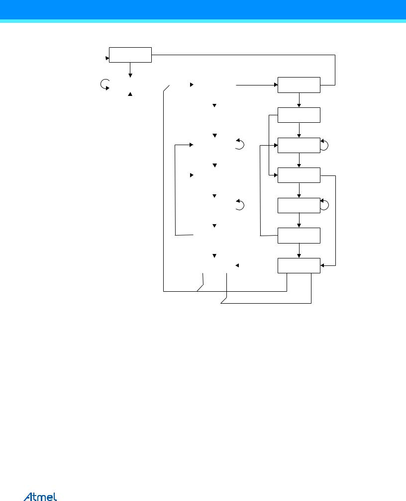
Figure 30-16. State Machine Sequence for Changing/Reading the Data Word
1  Test-Logic-Reset
|
0 |
|
|
|
|
|
|
|
|
|
0 |
|
|
1 |
|
|
|
|
|
1 |
|
Run-Test/Idle |
|
Select-DR Scan |
|
|||||||
|
|
|
|
|||||||
|
|
|
|
|
|
|
|
|
|
|
|
|
|
|
|
|
0 |
|
|
|
|
|
|
|
|
1 |
|
|
|
|
1 |
|
|
|
|
|
Capture-DR |
|
|||||
|
|
|
|
|
|
|
|
|||
|
|
|
|
|
|
|
|
|
|
|
|
|
|
|
|
|
0 |
|
|
|
|
|
|
|
|
|
|
|
|
|
|
|
|
|
|
|
|
Shift-DR |
|
0 |
|
||
|
|
|
|
|
|
|
|
|
|
|
|
|
|
|
|
|
1 |
|
|
|
|
|
|
|
|
|
|
|
|
|
1 |
|
|
|
|
|
|
Exit1-DR |
|
|
|||
|
|
|
|
|
|
|
|
|||
|
|
|
|
|
|
|
|
|
|
|
|
|
|
|
|
|
0 |
|
|
|
|
|
|
|
|
|
|
|
|
|
|
|
|
|
|
|
|
|
|
|
|
|
|
|
|
|
|
|
Pause-DR |
|
0 |
|
||
|
|
|
|
|
|
|
|
|
|
|
|
|
|
|
|
|
1 |
|
|
|
|
|
|
|
|
0 |
|
|
|
|
|
0 |
|
|
|
|
Exit2-DR |
|
|
||||
|
|
|
|
|
|
|
|
|||
|
|
|
|
|
|
|
|
|
|
|
|
|
|
|
|
|
1 |
|
|
|
|
|
|
|
|
|
|
|
|
|
|
|
|
|
|
|
|
Update-DR |
|
|
|
||
|
|
|
|
|
|
|
|
|||
|
|
|
|
|
|
|
|
|
|
|
|
|
|
|
|
1 |
|
|
0 |
|
|
|
|
|
|
|
|
|
|
|
|
|
1
Select-IR Scan
0
Capture-IR |
|
0 |
|
Shift-IR |
0 |
1 |
|
Exit1-IR |
1 |
|
|
0 |
|
Pause-IR |
0 |
1 |
|
Exit2-IR |
|
1 |
|
Update-IR |
|
1 |
0 |
30.9.11Flash Data Byte Register
The Flash Data Byte Register provides an efficient way to load the entire Flash page buffer before executing Page Write, or to read out/verify the content of the Flash. A state machine sets up the control signals to the Flash and senses the strobe signals from the Flash, thus only the data words need to be shifted in/out.
The Flash Data Byte Register actually consists of the 8-bit scan chain and a 8-bit temporary register. During page load, the Update-DR state copies the content of the scan chain over to the temporary register and initiates a write sequence that within 11 TCK cycles loads the content of the temporary register into the Flash page buffer. The AVR automatically alternates between writing the low and the high byte for each new Update-DR state, starting with the low byte for the first Update-DR encountered after entering the PROG_PAGELOAD command. The Program Counter is pre-incremented before writing the low byte, except for the first written byte. This ensures that the first data is written to the address set up by PROG_COMMANDS, and loading the last location in the page buffer does not make the Program Counter increment into the next page.
During Page Read, the content of the selected Flash byte is captured into the Flash Data Byte Register during the Capture-DR state. The AVR automatically alternates between reading the low and the high byte for each new Cap- ture-DR state, starting with the low byte for the first Capture-DR encountered after entering the PROG_PAGEREAD command. The Program Counter is post-incremented after reading each high byte, including the first read byte. This ensures that the first data is captured from the first address set up by PROG_COMMANDS, and reading the last location in the page makes the program counter increment into the next page.
ATmega640/V-1280/V-1281/V-2560/V-2561/V [DATASHEET] |
350 |
2549Q–AVR–02/2014
Figure 30-17. Flash Data Byte Register
STROBES
State
Machine
TDI
ADDRESS
Flash
EEPROM
Fuses
Lock Bits
D
A
T
A
TDO
The state machine controlling the Flash Data Byte Register is clocked by TCK. During normal operation in which eight bits are shifted for each Flash byte, the clock cycles needed to navigate through the TAP controller automatically feeds the state machine for the Flash Data Byte Register with sufficient number of clock pulses to complete its operation transparently for the user. However, if too few bits are shifted between each Update-DR state during page load, the TAP controller should stay in the Run-Test/Idle state for some TCK cycles to ensure that there are at least 11 TCK cycles between each Update-DR state.
30.9.12Programming Algorithm
All references below of type “1a”, “1b”, and so on, refer to Table 30-18 on page 347.
30.9.13Entering Programming Mode
1.Enter JTAG instruction AVR_RESET and shift 1 in the Reset Register.
2.Enter instruction PROG_ENABLE and shift 0b1010_0011_0111_0000 in the Programming Enable Register.
30.9.14Leaving Programming Mode
1.Enter JTAG instruction PROG_COMMANDS.
2.Disable all programming instructions by using no operation instruction 11a.
3.Enter instruction PROG_ENABLE and shift 0b0000_0000_0000_0000 in the programming Enable Register.
4.Enter JTAG instruction AVR_RESET and shift 0 in the Reset Register.
30.9.15Performing Chip Erase
1.Enter JTAG instruction PROG_COMMANDS.
2.Start Chip Erase using programming instruction 1a.
3.Poll for Chip Erase complete using programming instruction 1b, or wait for tWLRH_CE (refer to Table 30-14 on page 338).
ATmega640/V-1280/V-1281/V-2560/V-2561/V [DATASHEET] |
351 |
2549Q–AVR–02/2014

30.9.16Programming the Flash
Before programming the Flash a Chip Erase must be performed, see “Performing Chip Erase” on page 351.
1.Enter JTAG instruction PROG_COMMANDS.
2.Enable Flash write using programming instruction 2a.
3.Load address Extended High byte using programming instruction 2b.
4.Load address High byte using programming instruction 2c.
5.Load address Low byte using programming instruction 2d.
6.Load data using programming instructions 2e, 2f and 2g.
7.Repeat steps 5 and 6 for all instruction words in the page.
8.Write the page using programming instruction 2h.
9.Poll for Flash write complete using programming instruction 2i, or wait for tWLRH (refer to Table 30-14 on page 338).
10.Repeat steps 3 to 9 until all data have been programmed.
A more efficient data transfer can be achieved using the PROG_PAGELOAD instruction:
1.Enter JTAG instruction PROG_COMMANDS.
2.Enable Flash write using programming instruction 2a.
3.Load the page address using programming instructions 2b, 2c and 2d. PCWORD (refer to Table 30-7 on page 328) is used to address within one page and must be written as 0.
4.Enter JTAG instruction PROG_PAGELOAD.
5.Load the entire page by shifting in all instruction words in the page byte-by-byte, starting with the LSB of the first instruction in the page and ending with the MSB of the last instruction in the page. Use Update-DR to copy the contents of the Flash Data Byte Register into the Flash page location and to auto-increment the Program Counter before each new word.
6.Enter JTAG instruction PROG_COMMANDS.
7.Write the page using programming instruction 2h.
8.Poll for Flash write complete using programming instruction 2i, or wait for tWLRH (refer to Table 30-14 on page 338).
9.Repeat steps 3 to 8 until all data have been programmed.
30.9.17Reading the Flash
1.Enter JTAG instruction PROG_COMMANDS.
2.Enable Flash read using programming instruction 3a.
3.Load address using programming instructions 3b, 3c and 3d.
4.Read data using programming instruction 3e.
5.Repeat steps 3 and 4 until all data have been read.
A more efficient data transfer can be achieved using the PROG_PAGEREAD instruction:
1.Enter JTAG instruction PROG_COMMANDS.
2.Enable Flash read using programming instruction 3a.
3.Load the page address using programming instructions 3b, 3c and 3d. PCWORD (refer to Table 30-7 on page 328) is used to address within one page and must be written as 0.
4.Enter JTAG instruction PROG_PAGEREAD.
5.Read the entire page (or Flash) by shifting out all instruction words in the page (or Flash), starting with the LSB of the first instruction in the page (Flash) and ending with the MSB of the last instruction in the page (Flash). The Capture-DR state both captures the data from the Flash, and also auto-increments the program counter after each word is read. Note that Capture-DR comes before the shift-DR state. Hence, the first byte which is shifted out contains valid data.
ATmega640/V-1280/V-1281/V-2560/V-2561/V [DATASHEET] |
352 |
2549Q–AVR–02/2014

6.Enter JTAG instruction PROG_COMMANDS.
7.Repeat steps 3 to 6 until all data have been read.
30.9.18Programming the EEPROM
Before programming the EEPROM a Chip Erase must be performed, see “Performing Chip Erase” on page 351.
1.Enter JTAG instruction PROG_COMMANDS.
2.Enable EEPROM write using programming instruction 4a.
3.Load address High byte using programming instruction 4b.
4.Load address Low byte using programming instruction 4c.
5.Load data using programming instructions 4d and 4e.
6.Repeat steps 4 and 5 for all data bytes in the page.
7.Write the data using programming instruction 4f.
8.Poll for EEPROM write complete using programming instruction 4g, or wait for tWLRH (refer to Table 30-14 on page 338).
9.Repeat steps 3 to 8 until all data have been programmed.
Note that the PROG_PAGELOAD instruction can not be used when programming the EEPROM.
30.9.19Reading the EEPROM
1.Enter JTAG instruction PROG_COMMANDS.
2.Enable EEPROM read using programming instruction 5a.
3.Load address using programming instructions 5b and 5c.
4.Read data using programming instruction 5d.
5.Repeat steps 3 and 4 until all data have been read.
Note that the PROG_PAGEREAD instruction can not be used when reading the EEPROM.
30.9.20Programming the Fuses
1.Enter JTAG instruction PROG_COMMANDS.
2.Enable Fuse write using programming instruction 6a.
3.Load data high byte using programming instructions 6b. A bit value of “0” will program the corresponding fuse, a “1” will unprogram the fuse.
4.Write Fuse High byte using programming instruction 6c.
5.Poll for Fuse write complete using programming instruction 6d, or wait for tWLRH (refer to Table 30-14 on page 338).
6.Load data low byte using programming instructions 6e. A “0” will program the fuse, a “1” will unprogram the fuse.
7.Write Fuse low byte using programming instruction 6f.
8.Poll for Fuse write complete using programming instruction 6g, or wait for tWLRH (refer to Table 30-14 on page 338).
30.9.21Programming the Lock Bits
1.Enter JTAG instruction PROG_COMMANDS.
2.Enable Lock bit write using programming instruction 7a.
3.Load data using programming instructions 7b. A bit value of “0” will program the corresponding lock bit, a “1” will leave the lock bit unchanged.
4.Write Lock bits using programming instruction 7c.
5.Poll for Lock bit write complete using programming instruction 7d, or wait for tWLRH (refer to Table 30-14 on page 338).
ATmega640/V-1280/V-1281/V-2560/V-2561/V [DATASHEET] |
353 |
2549Q–AVR–02/2014