

- •1. Pin Configurations
- •2. Overview
- •2.1 Block Diagram
- •2.2 Comparison Between ATmega1281/2561 and ATmega640/1280/2560
- •2.3 Pin Descriptions
- •2.3.3 Port A (PA7..PA0)
- •2.3.4 Port B (PB7..PB0)
- •2.3.5 Port C (PC7..PC0)
- •2.3.6 Port D (PD7..PD0)
- •2.3.7 Port E (PE7..PE0)
- •2.3.8 Port F (PF7..PF0)
- •2.3.9 Port G (PG5..PG0)
- •2.3.10 Port H (PH7..PH0)
- •2.3.11 Port J (PJ7..PJ0)
- •2.3.12 Port K (PK7..PK0)
- •2.3.13 Port L (PL7..PL0)
- •2.3.14 RESET
- •2.3.15 XTAL1
- •2.3.16 XTAL2
- •2.3.17 AVCC
- •2.3.18 AREF
- •3. Resources
- •4. About Code Examples
- •5. Data Retention
- •6. Capacitive touch sensing
- •7. AVR CPU Core
- •7.1 Introduction
- •7.2 Architectural Overview
- •7.3 ALU – Arithmetic Logic Unit
- •7.4 Status Register
- •7.4.1 SREG – AVR Status Register
- •7.5 General Purpose Register File
- •7.6 Stack Pointer
- •7.6.2 EIND – Extended Indirect Register
- •7.7 Instruction Execution Timing
- •7.8 Reset and Interrupt Handling
- •7.8.1 Interrupt Response Time
- •8. AVR Memories
- •8.2 SRAM Data Memory
- •8.2.1 Data Memory Access Times
- •8.3 EEPROM Data Memory
- •8.3.1 EEPROM Read/Write Access
- •8.3.2 Preventing EEPROM Corruption
- •8.4 I/O Memory
- •8.4.1 General Purpose I/O Registers
- •9. External Memory Interface
- •9.1 Overview
- •9.1.1 Using the External Memory Interface
- •9.1.2 Address Latch Requirements
- •9.1.4 Timing
- •9.1.5 Using all Locations of External Memory Smaller than 64Kbytes
- •9.1.6 Using all 64Kbytes Locations of External Memory
- •9.2 Register Description
- •9.2.1 EEPROM registers
- •9.3 General Purpose registers
- •9.3.1 GPIOR2 – General Purpose I/O Register 2
- •9.3.2 GPIOR1 – General Purpose I/O Register 1
- •9.3.3 GPIOR0 – General Purpose I/O Register 0
- •9.4 External Memory registers
- •9.4.1 XMCRA – External Memory Control Register A
- •9.4.2 XMCRB – External Memory Control Register B
- •10. System Clock and Clock Options
- •10.1 Overview
- •10.2 Clock Systems and their Distribution
- •10.3 Clock Sources
- •10.3.1 Default Clock Source
- •10.4 Low Power Crystal Oscillator
- •10.5 Full Swing Crystal Oscillator
- •10.6 Low Frequency Crystal Oscillator
- •10.7 Calibrated Internal RC Oscillator
- •10.8 128kHz Internal Oscillator
- •10.9 External Clock
- •10.10 Clock Output Buffer
- •10.11 Timer/Counter Oscillator
- •10.12 System Clock Prescaler
- •10.13 Register Description
- •10.13.1 OSCCAL – Oscillator Calibration Register
- •10.13.2 CLKPR – Clock Prescale Register
- •11. Power Management and Sleep Modes
- •11.1 Sleep Modes
- •11.2 Idle Mode
- •11.3 ADC Noise Reduction Mode
- •11.6 Standby Mode
- •11.7 Extended Standby Mode
- •11.8 Power Reduction Register
- •11.9 Minimizing Power Consumption
- •11.9.1 Analog to Digital Converter
- •11.9.2 Analog Comparator
- •11.9.4 Internal Voltage Reference
- •11.9.5 Watchdog Timer
- •11.9.6 Port Pins
- •11.10 Register Description
- •11.10.1 SMCR – Sleep Mode Control Register
- •11.10.2 PRR0 – Power Reduction Register 0
- •11.10.3 PRR1 – Power Reduction Register 1
- •12. System Control and Reset
- •12.1 Resetting the AVR
- •12.2 Reset Sources
- •12.2.1 Power-on Reset
- •12.2.2 External Reset
- •12.2.4 Watchdog Reset
- •12.3 Internal Voltage Reference
- •12.4 Watchdog Timer
- •12.4.1 Features
- •12.4.2 Overview
- •12.5 Register Description
- •12.5.1 MCUSR – MCU Status Register
- •12.5.2 WDTCSR – Watchdog Timer Control Register
- •13. I/O-Ports
- •13.1 Introduction
- •13.2 Ports as General Digital I/O
- •13.2.1 Configuring the Pin
- •13.2.2 Toggling the Pin
- •13.2.3 Switching Between Input and Output
- •13.2.4 Reading the Pin Value
- •13.2.5 Digital Input Enable and Sleep Modes
- •13.2.6 Unconnected Pins
- •13.3 Alternate Port Functions
- •13.3.1 Alternate Functions of Port A
- •13.3.2 Alternate Functions of Port B
- •13.3.3 Alternate Functions of Port C
- •13.3.4 Alternate Functions of Port D
- •13.3.5 Alternate Functions of Port E
- •13.3.6 Alternate Functions of Port F
- •13.3.7 Alternate Functions of Port G
- •13.3.8 Alternate Functions of Port H
- •13.3.9 Alternate Functions of Port J
- •13.3.10 Alternate Functions of Port K
- •13.3.11 Alternate Functions of Port L
- •13.4.1 MCUCR – MCU Control Register
- •13.4.2 PORTA – Port A Data Register
- •13.4.3 DDRA – Port A Data Direction Register
- •13.4.4 PINA – Port A Input Pins Address
- •13.4.5 PORTB – Port B Data Register
- •13.4.6 DDRB – Port B Data Direction Register
- •13.4.7 PINB – Port B Input Pins Address
- •13.4.8 PORTC – Port C Data Register
- •13.4.9 DDRC – Port C Data Direction Register
- •13.4.10 PINC– Port C Input Pins Address
- •13.4.11 PORTD – Port D Data Register
- •13.4.12 DDRD – Port D Data Direction Register
- •13.4.13 PIND – Port D Input Pins Address
- •13.4.14 PORTE – Port E Data Register
- •13.4.15 DDRE – Port E Data Direction Register
- •13.4.16 PINE – Port E Input Pins Address
- •13.4.17 PORTF – Port F Data Register
- •13.4.18 DDRF – Port F Data Direction Register
- •13.4.19 PINF – Port F Input Pins Address
- •13.4.20 PORTG – Port G Data Register
- •13.4.21 DDRG – Port G Data Direction Register
- •13.4.22 PING – Port G Input Pins Address
- •13.4.23 PORTH – Port H Data Register
- •13.4.24 DDRH – Port H Data Direction Register
- •13.4.25 PINH – Port H Input Pins Address
- •13.4.26 PORTJ – Port J Data Register
- •13.4.27 DDRJ – Port J Data Direction Register
- •13.4.28 PINJ – Port J Input Pins Address
- •13.4.29 PORTK – Port K Data Register
- •13.4.30 DDRK – Port K Data Direction Register
- •13.4.31 PINK – Port K Input Pins Address
- •13.4.32 PORTL – Port L Data Register
- •13.4.33 DDRL – Port L Data Direction Register
- •13.4.34 PINL – Port L Input Pins Address
- •14. Interrupts
- •14.1 Interrupt Vectors in ATmega640/1280/1281/2560/2561
- •14.2 Reset and Interrupt Vector placement
- •14.3 Moving Interrupts Between Application and Boot Section
- •14.4 Register Description
- •14.4.1 MCUCR – MCU Control Register
- •15. External Interrupts
- •15.1 Pin Change Interrupt Timing
- •15.2 Register Description
- •15.2.1 EICRA – External Interrupt Control Register A
- •15.2.2 EICRB – External Interrupt Control Register B
- •15.2.3 EIMSK – External Interrupt Mask Register
- •15.2.4 EIFR – External Interrupt Flag Register
- •15.2.5 PCICR – Pin Change Interrupt Control Register
- •15.2.6 PCIFR – Pin Change Interrupt Flag Register
- •15.2.7 PCMSK2 – Pin Change Mask Register 2
- •15.2.8 PCMSK1 – Pin Change Mask Register 1
- •15.2.9 PCMSK0 – Pin Change Mask Register 0
- •16. 8-bit Timer/Counter0 with PWM
- •16.1 Features
- •16.2 Overview
- •16.2.1 Registers
- •16.2.2 Definitions
- •16.3 Timer/Counter Clock Sources
- •16.4 Counter Unit
- •16.5 Output Compare Unit
- •16.5.1 Force Output Compare
- •16.5.2 Compare Match Blocking by TCNT0 Write
- •16.5.3 Using the Output Compare Unit
- •16.6 Compare Match Output Unit
- •16.6.1 Compare Output Mode and Waveform Generation
- •16.7 Modes of Operation
- •16.7.1 Normal Mode
- •16.7.2 Clear Timer on Compare Match (CTC) Mode
- •16.7.3 Fast PWM Mode
- •16.7.4 Phase Correct PWM Mode
- •16.8 Timer/Counter Timing Diagrams
- •16.9 Register Description
- •16.9.1 TCCR0A – Timer/Counter Control Register A
- •16.9.2 TCCR0B – Timer/Counter Control Register B
- •16.9.3 TCNT0 – Timer/Counter Register
- •16.9.4 OCR0A – Output Compare Register A
- •16.9.5 OCR0B – Output Compare Register B
- •16.9.6 TIMSK0 – Timer/Counter Interrupt Mask Register
- •16.9.7 TIFR0 – Timer/Counter 0 Interrupt Flag Register
- •17. 16-bit Timer/Counter (Timer/Counter 1, 3, 4, and 5)
- •17.1 Features
- •17.2 Overview
- •17.2.1 Registers
- •17.2.2 Definitions
- •17.3.1 Reusing the Temporary High Byte Register
- •17.4 Timer/Counter Clock Sources
- •17.5 Counter Unit
- •17.6 Input Capture Unit
- •17.6.1 Input Capture Trigger Source
- •17.6.2 Noise Canceler
- •17.6.3 Using the Input Capture Unit
- •17.7 Output Compare Units
- •17.7.1 Force Output Compare
- •17.7.2 Compare Match Blocking by TCNTn Write
- •17.7.3 Using the Output Compare Unit
- •17.8 Compare Match Output Unit
- •17.8.1 Compare Output Mode and Waveform Generation
- •17.9 Modes of Operation
- •17.9.1 Normal Mode
- •17.9.2 Clear Timer on Compare Match (CTC) Mode
- •17.9.3 Fast PWM Mode
- •17.9.4 Phase Correct PWM Mode
- •17.9.5 Phase and Frequency Correct PWM Mode
- •17.10 Timer/Counter Timing Diagrams
- •17.11 Register Description
- •17.11.1 TCCR1A – Timer/Counter 1 Control Register A
- •17.11.2 TCCR3A – Timer/Counter 3 Control Register A
- •17.11.3 TCCR4A – Timer/Counter 4 Control Register A
- •17.11.4 TCCR5A – Timer/Counter 5 Control Register A
- •17.11.5 TCCR1B – Timer/Counter 1 Control Register B
- •17.11.6 TCCR3B – Timer/Counter 3 Control Register B
- •17.11.7 TCCR4B – Timer/Counter 4 Control Register B
- •17.11.8 TCCR5B – Timer/Counter 5 Control Register B
- •17.11.9 TCCR1C – Timer/Counter 1 Control Register C
- •17.11.10 TCCR3C – Timer/Counter 3 Control Register C
- •17.11.11 TCCR4C – Timer/Counter 4 Control Register C
- •17.11.12 TCCR5C – Timer/Counter 5 Control Register C
- •17.11.13 TCNT1H and TCNT1L – Timer/Counter 1
- •17.11.14 TCNT3H and TCNT3L – Timer/Counter 3
- •17.11.15 TCNT4H and TCNT4L –Timer/Counter 4
- •17.11.16 TCNT5H and TCNT5L –Timer/Counter 5
- •17.11.17 OCR1AH and OCR1AL – Output Compare Register 1 A
- •17.11.18 OCR1BH and OCR1BL – Output Compare Register 1 B
- •17.11.19 OCR1CH and OCR1CL – Output Compare Register 1 C
- •17.11.20 OCR3AH and OCR3AL – Output Compare Register 3 A
- •17.11.21 OCR3BH and OCR3BL – Output Compare Register 3 B
- •17.11.22 OCR3CH and OCR3CL – Output Compare Register 3 C
- •17.11.23 OCR4AH and OCR4AL – Output Compare Register 4 A
- •17.11.24 OCR4BH and OCR4BL – Output Compare Register 4 B
- •17.11.25 OCR4CH and OCR4CL –Output Compare Register 4 C
- •17.11.26 OCR5AH and OCR5AL – Output Compare Register 5 A
- •17.11.27 OCR5BH and OCR5BL – Output Compare Register 5 B
- •17.11.28 OCR5CH and OCR5CL –Output Compare Register 5 C
- •17.11.29 ICR1H and ICR1L – Input Capture Register 1
- •17.11.30 ICR3H and ICR3L – Input Capture Register 3
- •17.11.31 ICR4H and ICR4L – Input Capture Register 4
- •17.11.32 ICR5H and ICR5L – Input Capture Register 5
- •17.11.33 TIMSK1 – Timer/Counter 1 Interrupt Mask Register
- •17.11.34 TIMSK3 – Timer/Counter 3 Interrupt Mask Register
- •17.11.35 TIMSK4 – Timer/Counter 4 Interrupt Mask Register
- •17.11.36 TIMSK5 – Timer/Counter 5 Interrupt Mask Register
- •17.11.37 TIFR1 – Timer/Counter1 Interrupt Flag Register
- •17.11.38 TIFR3 – Timer/Counter3 Interrupt Flag Register
- •17.11.39 TIFR4 – Timer/Counter4 Interrupt Flag Register
- •17.11.40 TIFR5 – Timer/Counter5 Interrupt Flag Register
- •18. Timer/Counter 0, 1, 3, 4, and 5 Prescaler
- •18.1 Internal Clock Source
- •18.2 Prescaler Reset
- •18.3 External Clock Source
- •18.4 Register Description
- •18.4.1 GTCCR – General Timer/Counter Control Register
- •19. Output Compare Modulator (OCM1C0A)
- •19.1 Overview
- •19.2 Description
- •19.2.1 Timing example
- •20. 8-bit Timer/Counter2 with PWM and Asynchronous Operation
- •20.1 Overview
- •20.1.1 Registers
- •20.1.2 Definitions
- •20.2 Timer/Counter Clock Sources
- •20.3 Counter Unit
- •20.4 Modes of Operation
- •20.4.1 Normal Mode
- •20.4.2 Clear Timer on Compare Match (CTC) Mode
- •20.4.3 Fast PWM Mode
- •20.4.4 Phase Correct PWM Mode
- •20.5 Output Compare Unit
- •20.5.1 Force Output Compare
- •20.5.2 Compare Match Blocking by TCNT2 Write
- •20.5.3 Using the Output Compare Unit
- •20.6 Compare Match Output Unit
- •20.6.1 Compare Output Mode and Waveform Generation
- •20.7 Timer/Counter Timing Diagrams
- •20.8 Asynchronous Operation of Timer/Counter2
- •20.9 Timer/Counter Prescaler
- •20.10 Register Description
- •20.10.2 TCCR2B – Timer/Counter Control Register B
- •20.10.3 TCNT2 – Timer/Counter Register
- •20.10.4 OCR2A – Output Compare Register A
- •20.10.5 OCR2B – Output Compare Register B
- •20.10.6 ASSR – Asynchronous Status Register
- •20.10.7 TIMSK2 – Timer/Counter2 Interrupt Mask Register
- •20.10.8 TIFR2 – Timer/Counter2 Interrupt Flag Register
- •20.10.9 GTCCR – General Timer/Counter Control Register
- •21. SPI – Serial Peripheral Interface
- •21.1 SS Pin Functionality
- •21.1.1 Slave Mode
- •21.1.2 Master Mode
- •21.1.3 Data Modes
- •21.2 Register Description
- •21.2.1 SPCR – SPI Control Register
- •21.2.2 SPSR – SPI Status Register
- •21.2.3 SPDR – SPI Data Register
- •22. USART
- •22.1 Features
- •22.2 Overview
- •22.3 Clock Generation
- •22.3.1 Internal Clock Generation – The Baud Rate Generator
- •22.3.2 Double Speed Operation (U2Xn)
- •22.3.3 External Clock
- •22.3.4 Synchronous Clock Operation
- •22.4 Frame Formats
- •22.4.1 Parity Bit Calculation
- •22.5 USART Initialization
- •22.6 Data Transmission – The USART Transmitter
- •22.6.1 Sending Frames with 5 to 8 Data Bit
- •22.6.2 Sending Frames with 9 Data Bit
- •22.6.3 Transmitter Flags and Interrupts
- •22.6.4 Parity Generator
- •22.6.5 Disabling the Transmitter
- •22.7 Data Reception – The USART Receiver
- •22.7.1 Receiving Frames with 5 to 8 Data Bits
- •22.7.2 Receiving Frames with 9 Data Bits
- •22.7.3 Receive Compete Flag and Interrupt
- •22.7.4 Receiver Error Flags
- •22.7.5 Parity Checker
- •22.7.6 Disabling the Receiver
- •22.7.7 Flushing the Receive Buffer
- •22.8 Asynchronous Data Reception
- •22.8.1 Asynchronous Clock Recovery
- •22.8.2 Asynchronous Data Recovery
- •22.8.3 Asynchronous Operational Range
- •22.9.1 Using MPCMn
- •22.10 Register Description
- •22.10.1 UDRn – USART I/O Data Register n
- •22.10.2 UCSRnA – USART Control and Status Register A
- •22.10.3 UCSRnB – USART Control and Status Register n B
- •22.10.4 UCSRnC – USART Control and Status Register n C
- •22.10.5 UBRRnL and UBRRnH – USART Baud Rate Registers
- •22.11 Examples of Baud Rate Setting
- •23. USART in SPI Mode
- •23.1 Overview
- •23.2 USART MSPIM vs. SPI
- •23.2.1 Clock Generation
- •23.3 SPI Data Modes and Timing
- •23.4 Frame Formats
- •23.4.1 USART MSPIM Initialization
- •23.5 Data Transfer
- •23.5.1 Transmitter and Receiver Flags and Interrupts
- •23.5.2 Disabling the Transmitter or Receiver
- •23.6 USART MSPIM Register Description
- •23.6.1 UDRn – USART MSPIM I/O Data Register
- •23.6.2 UCSRnA – USART MSPIM Control and Status Register n A
- •23.6.3 UCSRnB – USART MSPIM Control and Status Register n B
- •23.6.4 UCSRnC – USART MSPIM Control and Status Register n C
- •23.6.5 UBRRnL and UBRRnH – USART MSPIM Baud Rate Registers
- •24. 2-wire Serial Interface
- •24.1 Features
- •24.2.1 TWI Terminology
- •24.2.2 Electrical Interconnection
- •24.3 Data Transfer and Frame Format
- •24.3.1 Transferring Bits
- •24.3.2 START and STOP Conditions
- •24.3.3 Address Packet Format
- •24.3.4 Data Packet Format
- •24.3.5 Combining Address and Data Packets into a Transmission
- •24.5 Overview of the TWI Module
- •24.5.1 SCL and SDA Pins
- •24.5.2 Bit Rate Generator Unit
- •24.5.3 Bus Interface Unit
- •24.5.4 Address Match Unit
- •24.5.5 Control Unit
- •24.6 Using the TWI
- •24.7 Transmission Modes
- •24.7.1 Master Transmitter Mode
- •24.7.2 Master Receiver Mode
- •24.7.3 Slave Receiver Mode
- •24.7.4 Slave Transmitter Mode
- •24.7.5 Miscellaneous States
- •24.7.6 Combining Several TWI Modes
- •24.9 Register Description
- •24.9.1 TWBR – TWI Bit Rate Register
- •24.9.2 TWCR – TWI Control Register
- •24.9.3 TWSR – TWI Status Register
- •24.9.4 TWDR – TWI Data Register
- •24.9.5 TWAR – TWI (Slave) Address Register
- •24.9.6 TWAMR – TWI (Slave) Address Mask Register
- •25. AC – Analog Comparator
- •25.1 Analog Comparator Multiplexed Input
- •25.2 Register Description
- •25.2.1 ADCSRB – ADC Control and Status Register B
- •25.2.2 ACSR – Analog Comparator Control and Status Register
- •25.2.3 DIDR1 – Digital Input Disable Register 1
- •26. ADC – Analog to Digital Converter
- •26.1 Features
- •26.2 Operation
- •26.3 Starting a Conversion
- •26.4 Prescaling and Conversion Timing
- •26.4.1 Differential Channels
- •26.5 Changing Channel or Reference Selection
- •26.5.1 ADC Input Channels
- •26.5.2 ADC Voltage Reference
- •26.6 ADC Noise Canceler
- •26.6.1 Analog Input Circuitry
- •26.6.2 Analog Noise Canceling Techniques
- •26.6.3 Offset Compensation Schemes
- •26.6.4 ADC Accuracy Definitions
- •26.7 ADC Conversion Result
- •26.8 Register Description
- •26.8.1 ADMUX – ADC Multiplexer Selection Register
- •26.8.2 ADCSRB – ADC Control and Status Register B
- •26.8.3 ADCSRA – ADC Control and Status Register A
- •26.8.4 ADCL and ADCH – The ADC Data Register
- •26.8.5 ADCSRB – ADC Control and Status Register B
- •26.8.6 DIDR0 – Digital Input Disable Register 0
- •26.8.7 DIDR2 – Digital Input Disable Register 2
- •27. JTAG Interface and On-chip Debug System
- •27.1 Features
- •27.2 Overview
- •27.3 TAP - Test Access Port
- •27.3.1 TAP Controller
- •27.6.1 PRIVATE0; 0x8
- •27.6.2 PRIVATE1; 0x9
- •27.6.3 PRIVATE2; 0xA
- •27.6.4 PRIVATE3; 0xB
- •27.7 Using the JTAG Programming Capabilities
- •27.8 Bibliography
- •28. IEEE 1149.1 (JTAG) Boundary-scan
- •28.1 Features
- •28.2 System Overview
- •28.3 Data Registers
- •28.3.1 Bypass Register
- •28.3.2 Device Identification Register
- •28.3.3 Reset Register
- •28.4.1 EXTEST; 0x0
- •28.4.2 IDCODE; 0x1
- •28.4.3 SAMPLE_PRELOAD; 0x2
- •28.4.4 AVR_RESET; 0xC
- •28.4.5 BYPASS; 0xF
- •28.5.1 Scanning the Digital Port Pins
- •28.5.2 Scanning the RESET Pin
- •28.6.1 MCUCR – MCU Control Register
- •28.6.2 MCUSR – MCU Status Register
- •29. Boot Loader Support – Read-While-Write Self-Programming
- •29.1 Features
- •29.2 Application and Boot Loader Flash Sections
- •29.2.1 Application Section
- •29.2.2 BLS – Boot Loader Section
- •29.4 Boot Loader Lock Bits
- •29.4.1 Entering the Boot Loader Program
- •29.6.1 Performing Page Erase by SPM
- •29.6.2 Filling the Temporary Buffer (Page Loading)
- •29.6.3 Performing a Page Write
- •29.6.4 Using the SPM Interrupt
- •29.6.5 Consideration While Updating BLS
- •29.6.7 Setting the Boot Loader Lock Bits by SPM
- •29.6.8 EEPROM Write Prevents Writing to SPMCSR
- •29.6.9 Reading the Fuse and Lock Bits from Software
- •29.6.10 Reading the Signature Row from Software
- •29.6.11 Preventing Flash Corruption
- •29.6.12 Programming Time for Flash when Using SPM
- •29.6.13 Simple Assembly Code Example for a Boot Loader
- •29.6.14 ATmega640 Boot Loader Parameters
- •29.6.15 ATmega1280/1281 Boot Loader Parameters
- •29.6.16 ATmega2560/2561 Boot Loader Parameters
- •29.7 Register Description
- •29.7.1 SPMCSR – Store Program Memory Control and Status Register
- •30. Memory Programming
- •30.1 Program And Data Memory Lock Bits
- •30.2 Fuse Bits
- •30.2.1 Latching of Fuses
- •30.3 Signature Bytes
- •30.4 Calibration Byte
- •30.5 Page Size
- •30.6 Parallel Programming Parameters, Pin Mapping, and Commands
- •30.6.1 Signal Names
- •30.7 Parallel Programming
- •30.7.1 Enter Programming Mode
- •30.7.2 Considerations for Efficient Programming
- •30.7.3 Chip Erase
- •30.7.4 Programming the Flash
- •30.7.5 Programming the EEPROM
- •30.7.6 Reading the Flash
- •30.7.7 Reading the EEPROM
- •30.7.8 Programming the Fuse Low Bits
- •30.7.9 Programming the Fuse High Bits
- •30.7.10 Programming the Extended Fuse Bits
- •30.7.11 Programming the Lock Bits
- •30.7.12 Reading the Fuse and Lock Bits
- •30.7.13 Reading the Signature Bytes
- •30.7.14 Reading the Calibration Byte
- •30.7.15 Parallel Programming Characteristics
- •30.8 Serial Downloading
- •30.8.1 Serial Programming Pin Mapping
- •30.8.2 Serial Programming Algorithm
- •30.8.3 Serial Programming Instruction set
- •30.8.4 Serial Programming Characteristics
- •30.9 Programming via the JTAG Interface
- •30.9.1 Programming Specific JTAG Instructions
- •30.9.2 AVR_RESET (0xC)
- •30.9.3 PROG_ENABLE (0x4)
- •30.9.4 PROG_COMMANDS (0x5)
- •30.9.5 PROG_PAGELOAD (0x6)
- •30.9.6 PROG_PAGEREAD (0x7)
- •30.9.7 Data Registers
- •30.9.8 Reset Register
- •30.9.9 Programming Enable Register
- •30.9.10 Programming Command Register
- •30.9.11 Flash Data Byte Register
- •30.9.12 Programming Algorithm
- •30.9.13 Entering Programming Mode
- •30.9.14 Leaving Programming Mode
- •30.9.15 Performing Chip Erase
- •30.9.16 Programming the Flash
- •30.9.17 Reading the Flash
- •30.9.18 Programming the EEPROM
- •30.9.19 Reading the EEPROM
- •30.9.20 Programming the Fuses
- •30.9.21 Programming the Lock Bits
- •30.9.22 Reading the Fuses and Lock Bits
- •30.9.23 Reading the Signature Bytes
- •30.9.24 Reading the Calibration Byte
- •31. Electrical Characteristics
- •31.1 DC Characteristics
- •31.2 Speed Grades
- •31.3 Clock Characteristics
- •31.3.1 Calibrated Internal RC Oscillator Accuracy
- •31.3.2 External Clock Drive Waveforms
- •31.4 External Clock Drive
- •31.5 System and Reset Characteristics
- •31.7 SPI Timing Characteristics
- •31.8 ADC Characteristics – Preliminary Data
- •31.9 External Data Memory Timing
- •32. Typical Characteristics
- •32.1 Active Supply Current
- •32.2 Idle Supply Current
- •32.2.1 Supply Current of IO modules
- •32.5 Standby Supply Current
- •32.7 Pin Driver Strength
- •32.8 Pin Threshold and Hysteresis
- •32.9 BOD Threshold and Analog Comparator Offset
- •32.10 Internal Oscillator Speed
- •32.11 Current Consumption of Peripheral Units
- •32.12 Current Consumption in Reset and Reset Pulsewidth
- •33. Register Summary
- •34. Instruction Set Summary
- •35. Ordering Information
- •35.1 ATmega640
- •35.2 ATmega1280
- •35.3 ATmega1281
- •35.4 ATmega2560
- •35.5 ATmega2561
- •36. Packaging Information
- •37. Errata
- •37.1 ATmega640 rev. B
- •37.2 ATmega640 rev. A
- •37.3 ATmega1280 rev. B
- •37.4 ATmega1280 rev. A
- •37.5 ATmega1281 rev. B
- •37.6 ATmega1281 rev. A
- •37.7 ATmega2560 rev. F
- •37.8 ATmega2560 rev. E
- •37.9 ATmega2560 rev. D
- •37.10 ATmega2560 rev. C
- •37.11 ATmega2560 rev. B
- •37.12 ATmega2560 rev. A
- •37.13 ATmega2561 rev. F
- •37.14 ATmega2561 rev. E
- •37.15 ATmega2561 rev. D
- •37.16 ATmega2561 rev. C
- •37.17 ATmega2561 rev. B
- •37.18 ATmega2561 rev. A
- •38. Datasheet Revision History
8. AVR Memories
This section describes the different memories in the ATmega640/1280/1281/2560/2561. The AVR architecture has two main memory spaces, the Data Memory and the Program Memory space. In addition, the ATmega640/1280/1281/2560/2561 features an EEPROM Memory for data storage. All three memory spaces are linear and regular.
8.1In-System Reprogrammable Flash Program Memory
The ATmega640/1280/1281/2560/2561 contains 64K/128K/256K bytes On-chip In-System Reprogrammable Flash memory for program storage, see Figure 8-1. Since all AVR instructions are 16 bit or 32 bit wide, the Flash is organized as 32K/64K/128K × 16. For software security, the Flash Program memory space is divided into two sections, Boot Program section and Application Program section.
The Flash memory has an endurance of at least 10,000 write/erase cycles. The ATmega640/1280/1281/2560/2561 Program Counter (PC) is 15/16/17 bits wide, thus addressing the 32K/64K/128K program memory locations. The operation of Boot Program section and associated Boot Lock bits for software protection are described in detail in “Boot Loader Support – Read-While-Write Self-Programming” on page 310. “Memory Programming” on page 325 contains a detailed description on Flash data serial downloading using the SPI pins or the JTAG interface.
Constant tables can be allocated within the entire program memory address space (see the LPM – Load Program Memory instruction description and ELPM - Extended Load Program Memory instruction description).
Timing diagrams for instruction fetch and execution are presented in “Instruction Execution Timing” on page 16.
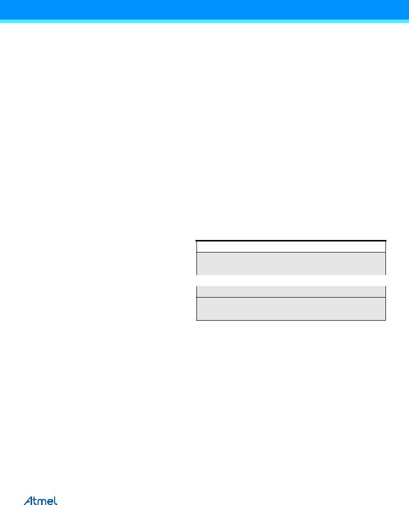
Figure 8-1. Program Flash Memory Map
Address (HEX)
0
Application Flash Section
Boot Flash Section
0x7FFF/0xFFFF/0x1FFFF
8.2SRAM Data Memory
Figure 8-2 on page 22 shows how the ATmega640/1280/1281/2560/2561 SRAM Memory is organized.
The ATmega640/1280/1281/2560/2561 is a complex microcontroller with more peripheral units than can be supported within the 64 location reserved in the Opcode for the IN and OUT instructions. For the Extended I/O space from $060 - $1FF in SRAM, only the ST/STS/STD and LD/LDS/LDD instructions can be used.
The first 4,608/8,704 Data Memory locations address both the Register File, the I/O Memory, Extended I/O Memory, and the internal data SRAM. The first 32 locations address the Register file, the next 64 location the standard I/O Memory, then 416 locations of Extended I/O memory and the next 8,192 locations address the internal data SRAM.
An optional external data SRAM can be used with the ATmega640/1280/1281/2560/2561. This SRAM will occupy an area in the remaining address locations in the 64K address space. This area starts at the address following the internal SRAM. The Register file, I/O, Extended I/O and Internal SRAM occupies the lowest 4,608/8,704 bytes, so when using 64Kbytes (65,536 bytes) of External Memory, 60,478/56,832 Bytes of External Memory are available. See “External Memory Interface” on page 27 for details on how to take advantage of the external memory map.
ATmega640/V-1280/V-1281/V-2560/V-2561/V [DATASHEET] |
20 |
2549Q–AVR–02/2014
When the addresses accessing the SRAM memory space exceeds the internal data memory locations, the external data SRAM is accessed using the same instructions as for the internal data memory access. When the internal data memories are accessed, the read and write strobe pins (PG0 and PG1) are inactive during the whole access cycle. External SRAM operation is enabled by setting the SRE bit in the XMCRA Register.
Accessing external SRAM takes one additional clock cycle per byte compared to access of the internal SRAM. This means that the commands LD, ST, LDS, STS, LDD, STD, PUSH, and POP take one additional clock cycle. If the Stack is placed in external SRAM, interrupts, subroutine calls and returns take three clock cycles extra because the three-byte program counter is pushed and popped, and external memory access does not take advantage of the internal pipe-line memory access. When external SRAM interface is used with wait-state, onebyte external access takes two, three, or four additional clock cycles for one, two, and three wait-states respectively. Interrupts, subroutine calls and returns will need five, seven, or nine clock cycles more than specified in the instruction set manual for one, two, and three wait-states.
The five different addressing modes for the data memory cover: Direct, Indirect with Displacement, Indirect, Indirect with Pre-decrement, and Indirect with Post-increment. In the Register file, registers R26 to R31 feature the indirect addressing pointer registers.
The direct addressing reaches the entire data space.
The Indirect with Displacement mode reaches 63 address locations from the base address given by the Y-register or Z-register.
When using register indirect addressing modes with automatic pre-decrement and post-increment, the address registers X, Y, and Z are decremented or incremented.
The 32 general purpose working registers, 64 I/O registers, and the 4,196/8,192 bytes of internal data SRAM in the ATmega640/1280/1281/2560/2561 are all accessible through all these addressing modes. The Register File is described in “General Purpose Register File” on page 13.
ATmega640/V-1280/V-1281/V-2560/V-2561/V [DATASHEET] |
21 |
2549Q–AVR–02/2014