
- •Ethernet Controller Features
- •Buffer
- •Physical Layer (PHY) Features
- •Operational
- •Package Types
- •Table of Contents
- •Most Current Data Sheet
- •Errata
- •Customer Notification System
- •1.0 Overview
- •FIGURE 1-1: ENC28J60 Block Diagram
- •FIGURE 1-2: Typical ENC28J60 Based Interface
- •2.0 External Connections
- •2.1 Oscillator
- •FIGURE 2-1: Crystal Oscillator Operation
- •2.3 CLKOUT Pin
- •FIGURE 2-3: CLKOUT Transition
- •2.4 Magnetics, Termination and Other External Components
- •FIGURE 2-4: ENC28J60 Ethernet Termination and External Connections
- •2.5 I/O Levels
- •2.6 LED Configuration
- •3.0 Memory Organization
- •3.1 Control Registers
- •3.1.1 ECON1 Register
- •3.1.2 ECON2 Register
- •Register 3-2: ECON2: Ethernet Control Register 2
- •3.2 Ethernet Buffer
- •3.2.1 Receive Buffer
- •3.2.2 Transmit Buffer
- •3.2.3 Reading and Writing to the Buffer
- •3.2.4 DMA Access to the Buffer
- •FIGURE 3-2: Ethernet Buffer Organization
- •3.3 PHY Registers
- •3.3.1 Reading PHY Registers
- •3.3.2 Writing PHY Registers
- •3.3.3 Scanning a PHY Register
- •Register 3-3: MICMD: MII Command Register
- •3.3.4 PHSTAT Registers
- •3.3.5 PHID1 and PHID2 Registers
- •4.0 Serial Peripheral Interface (SPI)
- •4.1 Overview
- •FIGURE 4-2: SPI Output Timing
- •4.2 SPI Instruction Set
- •4.2.1 Read Control Register Command
- •FIGURE 4-3: Read Control Register Command Sequence (ETH Registers)
- •FIGURE 4-4: Read Control Register Command Sequence (MAC and MII Registers)
- •4.2.2 Read Buffer Memory Command
- •4.2.3 Write Control Register Command
- •FIGURE 4-5: Write Control Register Command Sequence
- •4.2.4 Write Buffer Memory Command
- •4.2.5 Bit Field Set Command
- •4.2.6 Bit Field Clear Command
- •FIGURE 4-6: Write Buffer Memory Command Sequence
- •4.2.7 System Reset Command
- •FIGURE 4-7: System Reset Command Sequence
- •5.0 Ethernet Overview
- •5.1 Packet Format
- •5.1.2 Destination Address
- •5.1.3 Source Address
- •5.1.4 Type/Length
- •5.1.5 Data
- •5.1.6 Padding
- •6.0 Initialization
- •6.1 Receive Buffer
- •6.2 Transmit Buffer
- •6.3 Receive Filters
- •6.4 Waiting for OST
- •6.5 MAC Initialization Settings
- •Register 6-3: MACON4: MAC Control Register 4
- •Register 6-4: MABBIPG: MAC Back-to-back Inter-packet GAP Register
- •6.6 PHY Initialization Settings
- •7.0 Transmitting and Receiving Packets
- •7.1 Transmitting Packets
- •7.2 Receiving Packets
- •7.2.1 Enabling Reception
- •7.2.2 Receive Packet Layout
- •FIGURE 7-3: Sample Receive Packet Layout
- •7.2.3 Reading Received Packets
- •EXAMPLE 7-1: Random Access Address Calculation
- •7.2.4 Freeing Receive Buffer Space
- •7.2.5 Receive Buffer Free Space
- •EXAMPLE 7-2: Receive Buffer Free Space Calculation
- •8.0 Receive Filters
- •Register 8-1: ERXFCON: Ethernet RECEIVE FILTER CONTROL REGISTER
- •FIGURE 8-1: Receive Filtering Using OR Logic
- •FIGURE 8-2: Receive Filtering Using AND Logic
- •8.1 Unicast Filter
- •8.2 Pattern Match Filter
- •FIGURE 8-3: Sample Pattern Match Format
- •8.3 Magic Packet™ Filter
- •FIGURE 8-4: SAMPLE MAGIC PACKET™ Format
- •8.4 Hash Table Filter
- •8.5 Multicast Filter
- •8.6 Broadcast Filter
- •9.0 Duplex Mode Configuration and Negotiation
- •10.0 Flow Control
- •FIGURE 10-1: Sample Full-Duplex Network
- •Register 10-1: EFLOCON: Ethernet Flow Control Register
- •TABLE 10-1: Summary of Registers Used with Flow Control
- •11.0 Reset
- •FIGURE 11-1: On-Chip Reset Circuit
- •11.2 System Reset
- •11.3 Transmit Only Reset
- •11.4 Receive Only Reset
- •11.5 PHY Subsystem Reset
- •Register 11-1: PHCON1: PHY Control Register 1
- •12.0 Interrupts
- •FIGURE 12-1: ENC28J60 Interrupt Logic
- •12.1 INT Interrupt Enable (INTIE)
- •12.1.1 INT Interrupt Registers
- •Register 12-1: ESTAT: Ethernet Status Register
- •Register 12-2: EIE: Ethernet Interrupt Enable Register
- •Register 12-3: EIR: Ethernet Interrupt Request (Flag) Register
- •Register 12-4: PHIE: PHY Interrupt Enable Register
- •Register 12-5: PHIR: PHY Interrupt Request (Flag) Register
- •12.1.2 Receive Error Interrupt Flag (RXERIF)
- •12.1.3 Transmit Error Interrupt Flag (TXERIF)
- •12.1.4 Transmit Interrupt Flag (TXIF)
- •12.1.5 Link Change Interrupt Flag (LINKIF)
- •12.1.6 DMA Interrupt Flag (DMAIF)
- •12.1.7 Receive Packet Pending Interrupt Flag (PKTIF)
- •12.2.1 Setup Steps for Waking Up on a Magic Packet
- •13.0 Direct Memory Access Controller
- •13.1 Copying Memory
- •13.2 Checksum Calculations
- •TABLE 13-1: Summary of Registers Associated with the DMA Controller
- •14.0 Power-Down
- •TABLE 14-1: Summary of Registers Used with Power-Down
- •Register 15-1: EBSTCON: Ethernet SELF-TEST CONTROL REGISTER
- •15.1 Using the BIST
- •15.2 Random Data Fill Mode
- •15.3 Address Fill Mode
- •15.4 Pattern Shift Fill Mode
- •16.0 Electrical Characteristics
- •Absolute Maximum Ratings
- •16.1 DC Characteristics: ENC28J60 (Industrial and Commercial)
- •TABLE 16-1: AC Characteristics: ENC28J60 (Industrial and Commercial)
- •TABLE 16-2: Oscillator Timing Characteristics
- •TABLE 16-3: Reset AC Characteristics
- •TABLE 16-4: CLKOUT Pin AC Characteristics
- •TABLE 16-5: Requirements for External Magnetics
- •FIGURE 16-2: SPI Output Timing
- •TABLE 16-6: SPI Interface AC Characteristics
- •17.0 Packaging Information
- •17.1 Package Marking Information
- •17.2 Package Details
- •Appendix A: Revision History
- •Revision A (January 2006)
- •Revision B (July 2006)
- •Revision C (January 2008)
- •Revision D (July 2012)
- •Revision E (November 2012)
- •The Microchip Web Site
- •Customer Change Notification Service
- •Customer Support
- •Reader Response
- •INDEX
- •Product Identification System
- •Worldwide Sales and Service

ENC28J60
3.2Ethernet Buffer
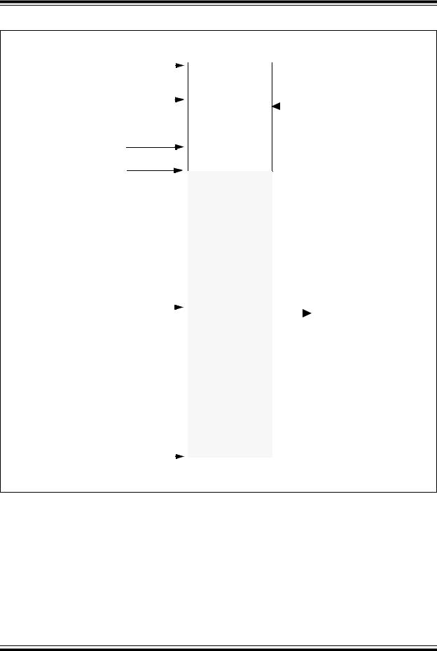
The Ethernet buffer contains transmit and receive memory used by the Ethernet controller. The entire buffer is 8 Kbytes, divided into separate receive and transmit buffer spaces. The sizes and locations of transmit and receive memory are fully programmable by the host controller using the SPI interface.
The relationship of the buffer spaces is shown in Figure 3-2.
3.2.1RECEIVE BUFFER
The receive buffer constitutes a circular FIFO buffer managed by hardware. The register pairs, ERXSTH:ERXSTL and ERXNDH:ERXNDL, serve as pointers to define the buffer’s size and location within the memory. The byte pointed to by ERXST and the byte pointed to by ERXND are both included in the FIFO buffer.
As bytes of data are received from the Ethernet interface, they are written into the receive buffer sequentially. However, after the memory pointed to by ERXND is written to, the hardware will automatically write the next byte of received data to the memory pointed to by ERXST. As a result, the receive hardware will never write outside the boundaries of the FIFO.
The host controller may program the ERXST and ERXND Pointers when the receive logic is not enabled. The pointers must not be modified while the receive logic is enabled (ECON1.RXEN is set). If desired, the Pointers may span the 1FFFh to 0000h memory boundary; the hardware will still operate as a FIFO.
The ERXWRPTH:ERXWRPTL registers define a location within the FIFO where the hardware will write bytes that it receives. The pointer is read-only and is automatically updated by the hardware whenever a new packet is successfully received. The pointer is useful for determining how much free space is available within the FIFO.
The ERXRDPT registers define a location within the FIFO where the receive hardware is forbidden to write to. In normal operation, the receive hardware will write data up to, but not including, the memory pointed to by ERXRDPT. If the FIFO fills up with data and new data continues to arrive, the hardware will not overwrite the previously received data. Instead, the new data will be thrown away and the old data will be preserved. In order to continuously receive new data, the host controller must periodically advance this pointer whenever it finishes processing some, or all, of the old received data.
3.2.2TRANSMIT BUFFER
Any space within the 8-Kbyte memory, which is not programmed as part of the receive FIFO buffer, is considered to be the transmit buffer. The responsibility of managing where packets are located in the transmit buffer belongs to the host controller. Whenever the host controller decides to transmit a packet, the ETXST and ETXND Pointers are programmed with addresses specifying where, within the transmit buffer, the particular packet to transmit is located. The hardware does not check that the start and end addresses do not overlap with the receive buffer. To prevent buffer corruption, the host controller must make sure to not transmit a packet while the ETXST and ETXND Pointers are overlapping the receive buffer, or while the ETXND Pointer is too close to the receive buffer. See
Section 7.1 “Transmitting Packets” for more information.
3.2.3READING AND WRITING TO THE BUFFER
The Ethernet buffer contents are accessed from the host controller though separate Read and Write Pointers (ERDPT and EWRPT) combined with the read buffer memory and write buffer memory SPI commands. While sequentially reading from the receive buffer, a wrapping condition will occur at the end of the receive buffer. While sequentially writing to the buffer, no wrapping conditions will occur. See
Section 4.2.2 “Read Buffer Memory Command” and Section 4.2.4 “Write Buffer Memory Command” for more information.
3.2.4DMA ACCESS TO THE BUFFER
The integrated DMA controller must read from the buffer when calculating a checksum and it must read and write to the buffer when copying memory. The DMA follows the same wrapping rules that SPI accesses do. While it sequentially reads, it will be subject to a wrapping condition at the end of the receive buffer. All writes it does will not be subject to any wrapping conditions. See
Section 13.0 “Direct Memory Access Controller” for more information.
2006-2012 Microchip Technology Inc. |
. |
DS39662E-page 17 |

ENC28J60
FIGURE 3-2: ETHERNET BUFFER ORGANIZATION
Transmit Buffer Start |
|
|
|
|
0000h |
||
|
|
||||||
|
|
|
|||||
(ETXSTH:ETXSTL) |
|
|
|
|
|
||
Buffer Write Pointer |
|
|
|
|
|
|
Transmit Buffer Data |
(EWRPTH:EWRPTL) |
AAh |
|
|
|
|||
|
|
|
(WBM AAh) |
||||
|
|
|
|
|
|
|
Transmit
Transmit Buffer End Buffer (ETXNDH:ETXNDL)
Receive Buffer Start (ERXSTH:ERXSTL)
|
|
|
Receive |
|
|
|
|
|
|
Buffer |
|
|
|
|
|
|
(Circular FIFO) |
|
|
|
Buffer Read Pointer |
|
|
|
|
|
Receive Buffer Data |
(ERDPTH:ERDPTL) |
|
|
55h |
|
|
|
|
|
|
|
(RBM 55h) |
||
|
|
|
|
|
|
Receive Buffer End |
|
|
|
1FFFh |
(ERXNDH:ERXNDL) |
|
|
DS39662E-page 18 |
. |
2006-2012 Microchip Technology Inc. |