

English for Masters
..pdffield-effect transistor. In fact, the device he had in mind was strikingly similar to one that Shockley was to suggest at Bell Labs a few months later.
16.In this scheme, an electric field from a metal plate should penetrate into a thin surface layer of a semiconductor strip beneath it, ripping electrons loose from their parent atoms to serve as current carriers. A voltage applied across the semiconductor strip would induce a current through it. Crucially, a varying voltage on the metal plate would modulate the current through the strip. Thus, small input signals would result in large output currents flowing through the strip. Or so Welker figured.
17.But tests he performed in March 1945 revealed no such amplification. In his logbook he recorded "only small effects," orders of magnitude less than what was predicted by Schottky's theory. Shockley, Brattain, and their Bell Labs colleagues attempted similar tests that very same spring, with similarly disappointing results.
18.The failures soon led Bardeen to postulate a novel idea of "surface states"—that free electrons were somehow huddling o n the semiconductor surface, shielding out the field. This conjecture, and Brattain's follow-up experiments to determine the physical nature of the surface states, led to their invention of the pointcontact transistor in December 1947—a month after t hey discovered how to overcome the shielding.
19.After his failures, Welker returned to research on germanium and resumed the theoretical studies of superconductivity he had reluctantly abandoned during the war. In 1946, British and French intelligence agents interrogated him about his involvement in German radar. They subsequently offered him an opportunity to work in Paris in an R&D operation set up under the auspices of a Westinghouse subsidiary, Compagnie des Freins et Signaux Westinghouse. The immediate goal was to manufacture germanium rectifiers for telecommunications and military electronics.
20.While teaching in Aachen at his alma mater in 1946, Mataré was also interviewed by agents. Fluent in French, he received a similar offer. He eagerly agreed to join the Paris effort, because doing research in devastated, occupied Germany was almost impossible.
70

21.Then in their mid-thirties, the two German physicists met in Paris and began organizing their operation...
22.With the rectifiers finally in production by late 1947, Welker resumed his research on superconductivity, while Mataré began to address the curious interference effects he had seen in germanium duodiodes during the war. When he put the two point contacts less than 100 mm apart, he again occasionally could get one of them to influence the other. With a positive voltage on one point, in fact, he could modulate and even amplify the electrical signal at the other! Mataré reckons he first recognized this effect in early 1948 (perhaps a month or two after Bardeen and Brattain's breakthrough at Bell Labs). But it still happened only sporadically.
23.On a hunch, he asked Welker to fashion larger germanium samples, from which they could cut slivers of higher purity. Using this higher-grade material, Mataré finally got consistent amplification in June 1948, six months after Bardeen and Brattain. Encouraged by this success, they phoned PTT Secretary Eugène Thomas and invited him over for a demonstration. But Thomas was apparently too busy—or perhaps not interested enough—to come by.
24.About that time, Welker put aside his theoretical work and tried to analyze what was going on just beneath the shiny germanium surface of Mataré's odd contraption. In an undated, handwritten document, now in the archives of Munich's Deutsches Museum, Welker speculated that one point— which he called the
"électrode de commande," or "control electrode"—was inducing strong electric fields in the germanium just beneath the other electrode, altering the material's conductivity there.
25. But Mataré was not buying that explanation, which followed the logic of Welker's unsuccessful 1945 attempt at a semiconductor amplifier... Mataré argued instead that the control electrode must be injecting positive charges, called holes, into the germanium. And perhaps by trickling along the boundary between two crystal grains, he guessed, they reached the other electrode—many micrometers distant . There they would bolster the conductivity under this electrode and enhance the
71
current through it. "Welker didn't really understand my measurements," Mataré says.
"At the time he was too busy studying superconductivity."...
26.But as the two men were debating the merits of their competing interpretations, surprising news arrived from across the Atlantic. In a 30 June press conference, Bell Labs suddenly lifted its six-month veil of secrecy and announced the invention of the transistor by Bardeen, Brattain, and Shockley. The breakthrough was reported in The New York Times on 1 July and published in the 15 July issue of Physical Review. Incredibly, the Bell Labs solid-state amplifier also had a pair of closely spaced metal points prodding into a germanium surface.
27.Mataré soon learned Bardeen and Brattain's explanation of the curious effects he had been observing. Electrons trapped on the germanium surface induce a shallow, positively charged layer just beneath it. Holes emitted by the control electrode (which they had dubbed the "emitter") travel easily within this layer over to the output electrode (or "collector"), markedly boosting the conductivity beneath it and therefore the current flowing through it.
28.After the Bell Labs revelations, Mataré and Welker had little difficulty getting the PTT minister to visit their lab. Thomas urged them to apply for a French patent on their semiconductor triode; he also suggested they call it by a slightly different name: transistron. So the two physicists hastily wrote up a patent disclosure and passed it on to the Westinghouse lawyers.
29.On 13 August, the company submitted a patent application for a "Nouveau système cristallin à plusieurs électrodes réalisant des effets de [sic] relais électroniques" to the Ministry of Industry and Commerce. Its brief description of what might be happening inside the germanium mostly followed Welker's field-effect interpretation but was probably influenced by Bardeen and Brattain's explanations.
30.By the May 1949 press conference, the two Germans had the device in limited production and were beginning to ship units for use by the PTT as amplifiers
in the telephone system—initially in the line betwe en Paris and Limoges. Speaking to the Paris press, Thomas compared these devices with vacuum tubes and demonstrated their use in radio receivers. Reporters hailed the two physicists as "les pères du
72
transistron" (the fathers of the transistron). The French device "turns out...to be superior to its American counterpart," read a more measured but still favorable account in Toute la Radio, a technical journal. "The latter has a limited lifetime and appears to be fairly unstable, whereas the existing transistrons do not show any sign of fatigue."
31. According to Mataré, this superiority could be attributed to the care they employed in fabricating their devices. While observing the process with microscopes, the women working on the small assembly line would measure current-voltage curves for both metal points with oscilloscopes and fix the points rigidly on the germanium with drops of epoxy after the curves matched the desired characteristics. When Brattain and Shockley visited the Paris group in 1950, Mataré showed them telephone amplifiers made with his transistrons—which allowed him to place a call all the way to Algiers. "That's quite something," admitted Shockley a bit guardedly, Mataré recalls half a century later.
32.But the French government and Westinghouse failed to capitalize on the technical advantages in semiconductors that they then appeared to have. After Hiroshima, nuclear physics had emerged as the dominant scientific discipline in the public mind, and nuclear power was widely heralded as the wave of the future. France became enchanted with pursuing the nuclear genie unbottled in the 1940s, while ignorant of its promising transistron.
33.Mataré and Welker struggled on in Paris for twomore years, but as support for their operation waned during the early 1950s, they started looking for jobs in their native land...
34.What is arguably the most important invention of the 20th century
remarkably occurred twice—and independently. Given the secrecy shrouding the Bell Labs device, there is no possibility Mataré and Welker could have been influenced by knowledge of it before July 1948, when news of the revolutionary invention became widespread. And it seems clear from the still-sketchy historical record that they indeed had a working, reliable amplifier by that time.
73
35. This dual, nearly simultaneous breakthrough can be attributed in part to the tremendous wartime advances in purifying silicon and, in particular, germanium. In both cases, germanium played the crucial gateway role, for in the immediate postwar years it could be refined much more easily and with substantially higher purities than silicon. Such high-purity semiconductor material was absolutely essential for fabricating the first transistors.
36. But the Bell Labs team had clear priority—and a superior physical understanding of how the electrons and holes were flowing inside germanium. That advantage proved critical to subsequent achievements, such as Shockley's junction transistor [see "The Lost History of the Transistor," IEEE Spectrum, May 2004], which was much easier to mass-produce with high reliability and uniformity. By the mid-1950s, nobody was trying to make point-contact transistors any longer, and the industry was moving on to silicon.
37.A factor crucial to success in the nascent semiconductor industry was the sustained innovation that flourished at Bell Labs—a s well as at Texas Instruments and Fairchild Semiconductor—leading to silicon tran sistors and integrated circuits. And that required extensive infrastructure, both material and intellectual, to keep these companies at the frontiers of this fast-moving field. Such an infrastructure already existed in the United States after World War II because of its wartime radar efforts. But France had no comparable infrastructure and had to import talent from occupied Germany, which could not exploit its own radar expertise until the 1950s.
38.In the absence of any such advantages, it was inevitable that Europe's fledgling transistor would soon be eclipsed by other, better semiconductor devices and eventually fade from memory.
Task 1. Find in the text examples of different types of participles. Translate them correctly.
Task 2. Analyze the underlined sentences from the grammatical point of view. Task 3. What do these terms mean? What do you know about them?
superheterodyne mixer, high-frequency radar signal, vacuum-tube diode,
solid-state crystal rectifier, microwave range, resistance, capacitance, rectifier,
74
oscillator, germanium duodiode, interference, solid-state amplifier, impurity, fieldeffect transistor, shielding, oscilloscope, current-voltage curve, light-emitting diode,
integrated circuit. |
|
|
Task 4. Match the synonyms. |
|
|
a) |
Crucial |
1) experience |
b) |
Candidly |
2) from time to time |
c) |
Remembrances |
3) go beyond |
d) |
Excess |
4) huge |
e) |
Occasionally |
5) important |
f) |
Boost |
6) memories |
g) |
Tremendous |
7) openly |
h) |
Nascent |
8) increase |
i) |
Expertise |
9) appearing |
Task 5. What parts of speech are these words? Divide them into groups: verbs, adverbs and nouns.
Uniformity, remembrance, occasionally, resemblance, hastily, purify, resume, revelation, flourish, validate, purity, validity, specification, ambiguity, variable, maintenance, embed.
Language skills.
Describing the process, the picture and the diagram.
Divide these groups of phrases into the categories:
1)introduction
2)describing the structure
3)describing the order
4)giving examples
5)expressing the result
6)making conclusions
a) to begin with… |
b)To sum up… |
c) such as… |
to start with… |
To conclude… |
for instance… |
firstly… secondly… |
Hence… |
like… |
75
I’d like to start with… |
Thereby… |
including… |
|
d) Due to … |
e) This diagram shows… |
f) It has… |
|
As the result of… |
On this diagram you can see… |
It’s divided into… |
|
Bring about … |
This table demonstrates… |
It consists of … |
|
Result in … |
This circle diagram illustrates … |
It is composed of… |
|
In response to…
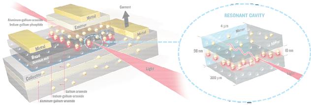
Task 1. These picture shows transistor laser. Read the information below the picture and describe it in your own words.
The semiconductor compounds we use in our transistor laser, gallium arsenide and indium-gallium-phosphide, readily produce photons. In these materials, which come from the III–V columns of the periodic table, the maximum energy in the valence band and the minimum energy in the conduction band occur at the same value of electron momentum. These III–V compounds a re known as direct-band-gap materials because an electron that has been excited into the conduction band can easily fall back to the valence band through the creation of a photon (of little momentum) whose energy matches the band-gap energy.
Photon emission is at the heart of every light-emitting diode. The simplest of semiconductor devices, a diode consists of two terminals and a single junction, called the p-n junction, between them. The p-n junction separates a region rich in conduction-band electrons (n-type material) from one that is rich in valence-band holes (p-type material). Applying a negative voltage to the n-type side pushes the
76
electrons across the junction into the region populated with holes. They recombine and emit light.
The basic structure of our transistor laser can be thought of as two back-to-back diodes separated by a thin connecting layer, a base layer. Called a bipolar junction transistor (BJT), it is one of two distinct families of transistors, the other being fieldeffect transistors.
Electrons that don't recombine with holes in the well or the base are swept into the collector, which exhibits a current gain. The device can be switched on and off billions of times per second and produces both optical and electrical signals.
The BJT is a direct descendant of Bardeen and Brattain's point-contact transistor and is so named because the main conduction channel uses both electrons and holes to carry the main electric current. It also shares the same names for the three terminals found on the point-contact transistor: emitter, base, and collector. Two p-n junctions exist inside the BJT: the collector-base junction and the base-emitter junction.
Discussion Matter.
Find information about identical inventions and report to the group. Include a picture or a diagram. Who do you think is a real inventor?
What do you know about patent writing? Study the following text and summarize its content.
How to Write the Description
Below are some how to instructions and tips to help get you started writing the description of your invention. When you are satisfied with the description you can begin the claims section of a patent application. Remember that the description and claims are the bulk of your written patent application.
77
∙
∙
∙
∙
∙
∙
∙
∙
When writing the description, use the following order, unless you can describe your invention better or more economically in another way. The order is:
title
technical field
background information and prior art
description of how your invention addresses a technical problem list of figures
detailed description of your invention one example of intended use
a sequence listing if relevant
To begin, it might be helpful to just jot down brief notes and points to cover from each of the above headings. As you polish your description into its final form, you can use the outline suggested below.
1.Begin on a new page by stating the title of your invention. Make it short, precise and specific. For example, if your invention is a compound, say "Carbon tetrachoride" not "Compound". Avoid calling the invention after yourself or using the words new or improved. Aim to give it a title that can be found by people using a few key words during a patent searching.
2.Then write a broad statement that gives the technical field related to your invention.
3.Continue by offering background information that people will need to: understand, search for, or examine, your invention.
4.Discuss the problems that inventors have faced in this area and how they have attempted to solve them. This is often called giving the prior art. Prior art is the published body of knowledge that relates to your invention. It is at this point that applicants frequently quote previous similar patents.
5.Then state in general terms how your invention solves one or several of these problems. What you are trying to show is how your invention is new and different.
78
6.List the drawings giving the figure number and a brief description of what the drawings illustrate. Remember to refer to drawings throughout the detailed description and to use the same reference numbers for each element.
7.Describe your intellectual property in detail. For an apparatus or product, describe each part, how they fit together and how they work together. For a process, describe each step, what you start with, what you need to do to make the change, and the end result. For a compound include the chemical formula, the structure and the process which could be used to make the compound. You need to make the description fit all the possible alternatives that relate to your invention. If a part can be made out of several different materials, say so. You should aim to describe each part in sufficient detail so that someone could reproduce at least one version of your invention.
8.Give an example of an intended use for your invention. You should also include any warnings of commonly used in the field that would be necessary to avert failure.
9.If relevant to your type of invention, provide the sequence listing of your compound. The sequence is part of the description and is not included with any drawings.
One of the best ways to understand how to write a patent for your type of invention is to take a look at already issued patents. Visit the USPTO online and do a search for patents issued for similar inventions to yours.
Module VI.
Grammar: Non-finite forms of the verbs. Gerund.
Language Skills: Subjunctive Mood.
Reading: Earthquake Alarm.
Discussion: Present day techniques and technology for predicting natural disasters.
79