

9. External Memory Interface
With all the features the External Memory Interface provides, it is well suited to operate as an interface to memory devices such as External SRAM and Flash, and peripherals such as LCD-display, A/D, and D/A. The main features are:
•Four different wait-state settings (including no wait-state)
•Independent wait-state setting for different External Memory sectors (configurable sector size)
•The number of bits dedicated to address high byte is selectable
•Bus keepers on data lines to minimize current consumption (optional)
9.1Overview
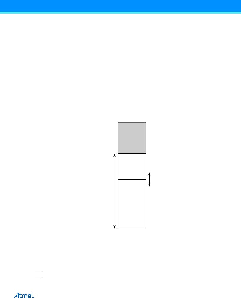
When the eXternal MEMory (XMEM) is enabled, address space outside the internal SRAM becomes available using the dedicated External Memory pins (see Figure 1-3 on page 4, Table 13-3 on page 75, Table 13-9 on page 79, and Table 13-21 on page 86). The memory configuration is shown in Figure 9-1.
Figure 9-1. External Memory with Sector Select
Memory Configuration A
0x0000
Internal memory
0x21FF
0x2200
Lower sector
SRW01
SRW00
SRL[2..0]
External Memory |
Upper sector |
|
(0 - 60K x 8) |
||
|
SRW11
SRW10
0xFFFF
9.1.1Using the External Memory Interface
The interface consists of:
•AD7:0: Multiplexed low-order address bus and data bus
A15:8: High-order address bus (configurable number of bits)
•ALE: Address latch enable
•RD: Read strobe
•WR: Write strobe
ATmega640/V-1280/V-1281/V-2560/V-2561/V [DATASHEET] |
27 |
2549Q–AVR–02/2014
The control bits for the External Memory Interface are located in two registers, the External Memory Control Register A – XMCRA, and the External Memory Control Register B – XMCRB.
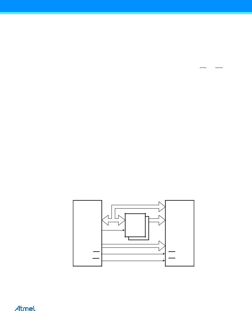
When the XMEM interface is enabled, the XMEM interface will override the setting in the data direction registers that corresponds to the ports dedicated to the XMEM interface. For details about the port override, see the alternate functions in section “I/O-Ports” on page 67. The XMEM interface will auto-detect whether an access is internal or external. If the access is external, the XMEM interface will output address, data, and the control signals on the ports according to Figure 9-3 on page 29 (this figure shows the wave forms without wait-states). When ALE goes from high-to-low, there is a valid address on AD7:0. ALE is low during a data transfer. When the XMEM interface is enabled, also an internal access will cause activity on address, data and ALE ports, but the RD and WR strobes will not toggle during internal access. When the External Memory Interface is disabled, the normal pin and data direction settings are used. Note that when the XMEM interface is disabled, the address space above the internal SRAM boundary is not mapped into the internal SRAM. Figure 9-2 illustrates how to connect an external SRAM to the AVR using an octal latch (typically “74 × 573” or equivalent) which is transparent when G is high.
9.1.2Address Latch Requirements
Due to the high-speed operation of the XRAM interface, the address latch must be selected with care for system frequencies above 8MHz @ 4V and 4MHz @ 2.7V. When operating at conditions above these frequencies, the typical old style 74HC series latch becomes inadequate. The External Memory Interface is designed in compliance to the 74AHC series latch. However, most latches can be used as long they comply with the main timing parameters. The main parameters for the address latch are:
•D to Q propagation delay (tPD)
•Data setup time before G low (tSU)
•Data (address) hold time after G low (TH)
The External Memory Interface is designed to guaranty minimum address hold time after G is asserted low of th =
5ns. Refer to tLAXX_LD/tLLAXX_ST in “External Data Memory Timing” Tables 31-11 through Tables 31-18 on pages 367 - 370. The D-to-Q propagation delay (tPD) must be taken into consideration when calculating the access time
requirement of the external component. The data setup time before G low (tSU) must not exceed address valid to ALE low (tAVLLC) minus PCB wiring delay (dependent on the capacitive load).
Figure 9-2. External SRAM Connected to the AVR
AVR |
SRAM |
|
|
|
D[7:0] |
AD7:0 |
D |
Q |
A[7:0] |
ALE |
G |
|
|
A15:8 |
|
|
A[15:8] |
RD |
|
|
RD |
WR |
|
|
WR |
ATmega640/V-1280/V-1281/V-2560/V-2561/V [DATASHEET] |
28 |
2549Q–AVR–02/2014
9.1.3Pull-up and Bus-keeper
The pull-ups on the AD7:0 ports may be activated if the corresponding Port register is written to one. To reduce power consumption in sleep mode, it is recommended to disable the pull-ups by writing the Port register to zero before entering sleep.
The XMEM interface also provides a bus-keeper on the AD7:0 lines. The bus-keeper can be disabled and enabled in software as described in “XMCRB – External Memory Control Register B” on page 38. When enabled, the buskeeper will keep the previous value on the AD7:0 bus while these lines are tri-stated by the XMEM interface.
9.1.4Timing
External Memory devices have different timing requirements. To meet these requirements, the XMEM interface provides four different wait-states as shown in Table 9-3 on page 37. It is important to consider the timing specification of the External Memory device before selecting the wait-state. The most important parameters are the access time for the external memory compared to the set-up requirement. The access time for the External Memory is defined to be the time from receiving the chip select/address until the data of this address actually is driven on the bus. The access time cannot exceed the time from the ALE pulse must be asserted low until data is stable during a
read sequence (see tLLRL+ tRLRH - tDVRH in Tables 31-11 through Tables 31-18 on pages 367 - 370). The different wait-states are set up in software. As an additional feature, it is possible to divide the external memory space in two
sectors with individual wait-state settings. This makes it possible to connect two different memory devices with different timing requirements to the same XMEM interface. For XMEM interface timing details, refer to Table 31-11 on page 367 to Table 31-18 on page 370 and Figure 31-9 on page 370 to Figure 31-12 on page 372 in the “External Data Memory Timing” on page 367.
Note that the XMEM interface is asynchronous and that the waveforms in the following figures are related to the internal system clock. The skew between the internal and external clock (XTAL1) is not guarantied (varies between devices temperature, and supply voltage). Consequently, the XMEM interface is not suited for synchronous operation.
Figure 9-3. External Data Memory Cycles without Wait-state (SRWn1=0 and SRWn0=0)(1)
|
T1 |
T2 |
|
T3 |
T4 |
System Clock (CLKCPU) |
|
|
|
|
|
ALE |
|
|
|
|
|
A15:8 |
Prev. addr. |
|
|
Address |
|
DA7:0 |
Prev. data |
Address |
XX |
Data |
|
WR |
|
|
|
|
|
DA7:0 (XMBK = 0) |
Prev. data |
Address |
|
Data |
|
DA7:0 (XMBK = 1) |
Prev. data |
Address |
XXXXX |
Data |
XXXXXXXX |
Write
Read
RD 
Note: 1. SRWn1 = SRW11 (upper sector) or SRW01 (lower sector), SRWn0 = SRW10 (upper sector) or SRW00 (lower sector). The ALE pulse in period T4 is only present if the next instruction accesses the RAM (internal or external).
ATmega640/V-1280/V-1281/V-2560/V-2561/V [DATASHEET] |
29 |
2549Q–AVR–02/2014
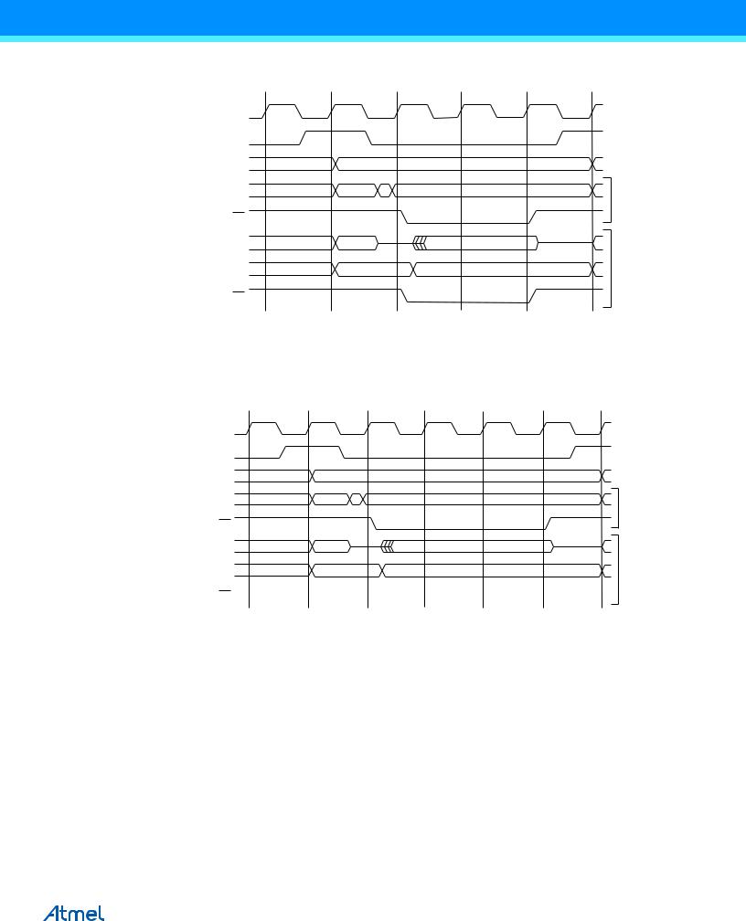
Figure 9-4. External Data Memory Cycles with SRWn1 = 0 and SRWn0 = 1(1)
|
T1 |
T2 |
T3 |
T4 |
T5 |
System Clock (CLKCPU) |
|
|
|
|
|
ALE |
|
|
|
|
|
A15:8 |
Prev. addr. |
|
Address |
|
|
DA7:0 |
Prev. data |
Address XX |
Data |
|
|
WR |
|
|
|
|
|
DA7:0 (XMBK = 0) |
Prev. data |
Address |
Data |
|
|
DA7:0 (XMBK = 1) |
Prev. data |
Address |
Data |
|
|
RD |
|
|
|
|
|
Read Write
Note: 1. SRWn1 = SRW11 (upper sector) or SRW01 (lower sector), SRWn0 = SRW10 (upper sector) or SRW00 (lower sector).
The ALE pulse in period T5 is only present if the next instruction accesses the RAM (internal or external).
Figure 9-5. External Data Memory Cycles with SRWn1 = 1 and SRWn0 = 0(1)
|
T1 |
T2 |
T3 |
T4 |
T5 |
T6 |
System Clock (CLKCPU) |
|
|
|
|
|
|
ALE |
|
|
|
|
|
|
A15:8 |
Prev. addr. |
|
Address |
|
|
|
DA7:0 |
Prev. data |
Address XX |
Data |
|
|
|
WR |
|
|
|
|
|
|
DA7:0 (XMBK = 0) |
Prev. data |
Address |
Data |
|
|
|
DA7:0 (XMBK = 1) |
Prev. data |
Address |
Data |
|
|
|
Read Write
RD 
Note: 1. SRWn1 = SRW11 (upper sector) or SRW01 (lower sector), SRWn0 = SRW10 (upper sector) or SRW00 (lower sector).
The ALE pulse in period T6 is only present if the next instruction accesses the RAM (internal or external).
ATmega640/V-1280/V-1281/V-2560/V-2561/V [DATASHEET] |
30 |
2549Q–AVR–02/2014