

- •1. Pin Configurations
- •2. Overview
- •2.1 Block Diagram
- •2.2 Comparison Between ATmega1281/2561 and ATmega640/1280/2560
- •2.3 Pin Descriptions
- •2.3.3 Port A (PA7..PA0)
- •2.3.4 Port B (PB7..PB0)
- •2.3.5 Port C (PC7..PC0)
- •2.3.6 Port D (PD7..PD0)
- •2.3.7 Port E (PE7..PE0)
- •2.3.8 Port F (PF7..PF0)
- •2.3.9 Port G (PG5..PG0)
- •2.3.10 Port H (PH7..PH0)
- •2.3.11 Port J (PJ7..PJ0)
- •2.3.12 Port K (PK7..PK0)
- •2.3.13 Port L (PL7..PL0)
- •2.3.14 RESET
- •2.3.15 XTAL1
- •2.3.16 XTAL2
- •2.3.17 AVCC
- •2.3.18 AREF
- •3. Resources
- •4. About Code Examples
- •5. Data Retention
- •6. Capacitive touch sensing
- •7. AVR CPU Core
- •7.1 Introduction
- •7.2 Architectural Overview
- •7.3 ALU – Arithmetic Logic Unit
- •7.4 Status Register
- •7.4.1 SREG – AVR Status Register
- •7.5 General Purpose Register File
- •7.6 Stack Pointer
- •7.6.2 EIND – Extended Indirect Register
- •7.7 Instruction Execution Timing
- •7.8 Reset and Interrupt Handling
- •7.8.1 Interrupt Response Time
- •8. AVR Memories
- •8.2 SRAM Data Memory
- •8.2.1 Data Memory Access Times
- •8.3 EEPROM Data Memory
- •8.3.1 EEPROM Read/Write Access
- •8.3.2 Preventing EEPROM Corruption
- •8.4 I/O Memory
- •8.4.1 General Purpose I/O Registers
- •9. External Memory Interface
- •9.1 Overview
- •9.1.1 Using the External Memory Interface
- •9.1.2 Address Latch Requirements
- •9.1.4 Timing
- •9.1.5 Using all Locations of External Memory Smaller than 64Kbytes
- •9.1.6 Using all 64Kbytes Locations of External Memory
- •9.2 Register Description
- •9.2.1 EEPROM registers
- •9.3 General Purpose registers
- •9.3.1 GPIOR2 – General Purpose I/O Register 2
- •9.3.2 GPIOR1 – General Purpose I/O Register 1
- •9.3.3 GPIOR0 – General Purpose I/O Register 0
- •9.4 External Memory registers
- •9.4.1 XMCRA – External Memory Control Register A
- •9.4.2 XMCRB – External Memory Control Register B
- •10. System Clock and Clock Options
- •10.1 Overview
- •10.2 Clock Systems and their Distribution
- •10.3 Clock Sources
- •10.3.1 Default Clock Source
- •10.4 Low Power Crystal Oscillator
- •10.5 Full Swing Crystal Oscillator
- •10.6 Low Frequency Crystal Oscillator
- •10.7 Calibrated Internal RC Oscillator
- •10.8 128kHz Internal Oscillator
- •10.9 External Clock
- •10.10 Clock Output Buffer
- •10.11 Timer/Counter Oscillator
- •10.12 System Clock Prescaler
- •10.13 Register Description
- •10.13.1 OSCCAL – Oscillator Calibration Register
- •10.13.2 CLKPR – Clock Prescale Register
- •11. Power Management and Sleep Modes
- •11.1 Sleep Modes
- •11.2 Idle Mode
- •11.3 ADC Noise Reduction Mode
- •11.6 Standby Mode
- •11.7 Extended Standby Mode
- •11.8 Power Reduction Register
- •11.9 Minimizing Power Consumption
- •11.9.1 Analog to Digital Converter
- •11.9.2 Analog Comparator
- •11.9.4 Internal Voltage Reference
- •11.9.5 Watchdog Timer
- •11.9.6 Port Pins
- •11.10 Register Description
- •11.10.1 SMCR – Sleep Mode Control Register
- •11.10.2 PRR0 – Power Reduction Register 0
- •11.10.3 PRR1 – Power Reduction Register 1
- •12. System Control and Reset
- •12.1 Resetting the AVR
- •12.2 Reset Sources
- •12.2.1 Power-on Reset
- •12.2.2 External Reset
- •12.2.4 Watchdog Reset
- •12.3 Internal Voltage Reference
- •12.4 Watchdog Timer
- •12.4.1 Features
- •12.4.2 Overview
- •12.5 Register Description
- •12.5.1 MCUSR – MCU Status Register
- •12.5.2 WDTCSR – Watchdog Timer Control Register
- •13. I/O-Ports
- •13.1 Introduction
- •13.2 Ports as General Digital I/O
- •13.2.1 Configuring the Pin
- •13.2.2 Toggling the Pin
- •13.2.3 Switching Between Input and Output
- •13.2.4 Reading the Pin Value
- •13.2.5 Digital Input Enable and Sleep Modes
- •13.2.6 Unconnected Pins
- •13.3 Alternate Port Functions
- •13.3.1 Alternate Functions of Port A
- •13.3.2 Alternate Functions of Port B
- •13.3.3 Alternate Functions of Port C
- •13.3.4 Alternate Functions of Port D
- •13.3.5 Alternate Functions of Port E
- •13.3.6 Alternate Functions of Port F
- •13.3.7 Alternate Functions of Port G
- •13.3.8 Alternate Functions of Port H
- •13.3.9 Alternate Functions of Port J
- •13.3.10 Alternate Functions of Port K
- •13.3.11 Alternate Functions of Port L
- •13.4.1 MCUCR – MCU Control Register
- •13.4.2 PORTA – Port A Data Register
- •13.4.3 DDRA – Port A Data Direction Register
- •13.4.4 PINA – Port A Input Pins Address
- •13.4.5 PORTB – Port B Data Register
- •13.4.6 DDRB – Port B Data Direction Register
- •13.4.7 PINB – Port B Input Pins Address
- •13.4.8 PORTC – Port C Data Register
- •13.4.9 DDRC – Port C Data Direction Register
- •13.4.10 PINC– Port C Input Pins Address
- •13.4.11 PORTD – Port D Data Register
- •13.4.12 DDRD – Port D Data Direction Register
- •13.4.13 PIND – Port D Input Pins Address
- •13.4.14 PORTE – Port E Data Register
- •13.4.15 DDRE – Port E Data Direction Register
- •13.4.16 PINE – Port E Input Pins Address
- •13.4.17 PORTF – Port F Data Register
- •13.4.18 DDRF – Port F Data Direction Register
- •13.4.19 PINF – Port F Input Pins Address
- •13.4.20 PORTG – Port G Data Register
- •13.4.21 DDRG – Port G Data Direction Register
- •13.4.22 PING – Port G Input Pins Address
- •13.4.23 PORTH – Port H Data Register
- •13.4.24 DDRH – Port H Data Direction Register
- •13.4.25 PINH – Port H Input Pins Address
- •13.4.26 PORTJ – Port J Data Register
- •13.4.27 DDRJ – Port J Data Direction Register
- •13.4.28 PINJ – Port J Input Pins Address
- •13.4.29 PORTK – Port K Data Register
- •13.4.30 DDRK – Port K Data Direction Register
- •13.4.31 PINK – Port K Input Pins Address
- •13.4.32 PORTL – Port L Data Register
- •13.4.33 DDRL – Port L Data Direction Register
- •13.4.34 PINL – Port L Input Pins Address
- •14. Interrupts
- •14.1 Interrupt Vectors in ATmega640/1280/1281/2560/2561
- •14.2 Reset and Interrupt Vector placement
- •14.3 Moving Interrupts Between Application and Boot Section
- •14.4 Register Description
- •14.4.1 MCUCR – MCU Control Register
- •15. External Interrupts
- •15.1 Pin Change Interrupt Timing
- •15.2 Register Description
- •15.2.1 EICRA – External Interrupt Control Register A
- •15.2.2 EICRB – External Interrupt Control Register B
- •15.2.3 EIMSK – External Interrupt Mask Register
- •15.2.4 EIFR – External Interrupt Flag Register
- •15.2.5 PCICR – Pin Change Interrupt Control Register
- •15.2.6 PCIFR – Pin Change Interrupt Flag Register
- •15.2.7 PCMSK2 – Pin Change Mask Register 2
- •15.2.8 PCMSK1 – Pin Change Mask Register 1
- •15.2.9 PCMSK0 – Pin Change Mask Register 0
- •16. 8-bit Timer/Counter0 with PWM
- •16.1 Features
- •16.2 Overview
- •16.2.1 Registers
- •16.2.2 Definitions
- •16.3 Timer/Counter Clock Sources
- •16.4 Counter Unit
- •16.5 Output Compare Unit
- •16.5.1 Force Output Compare
- •16.5.2 Compare Match Blocking by TCNT0 Write
- •16.5.3 Using the Output Compare Unit
- •16.6 Compare Match Output Unit
- •16.6.1 Compare Output Mode and Waveform Generation
- •16.7 Modes of Operation
- •16.7.1 Normal Mode
- •16.7.2 Clear Timer on Compare Match (CTC) Mode
- •16.7.3 Fast PWM Mode
- •16.7.4 Phase Correct PWM Mode
- •16.8 Timer/Counter Timing Diagrams
- •16.9 Register Description
- •16.9.1 TCCR0A – Timer/Counter Control Register A
- •16.9.2 TCCR0B – Timer/Counter Control Register B
- •16.9.3 TCNT0 – Timer/Counter Register
- •16.9.4 OCR0A – Output Compare Register A
- •16.9.5 OCR0B – Output Compare Register B
- •16.9.6 TIMSK0 – Timer/Counter Interrupt Mask Register
- •16.9.7 TIFR0 – Timer/Counter 0 Interrupt Flag Register
- •17. 16-bit Timer/Counter (Timer/Counter 1, 3, 4, and 5)
- •17.1 Features
- •17.2 Overview
- •17.2.1 Registers
- •17.2.2 Definitions
- •17.3.1 Reusing the Temporary High Byte Register
- •17.4 Timer/Counter Clock Sources
- •17.5 Counter Unit
- •17.6 Input Capture Unit
- •17.6.1 Input Capture Trigger Source
- •17.6.2 Noise Canceler
- •17.6.3 Using the Input Capture Unit
- •17.7 Output Compare Units
- •17.7.1 Force Output Compare
- •17.7.2 Compare Match Blocking by TCNTn Write
- •17.7.3 Using the Output Compare Unit
- •17.8 Compare Match Output Unit
- •17.8.1 Compare Output Mode and Waveform Generation
- •17.9 Modes of Operation
- •17.9.1 Normal Mode
- •17.9.2 Clear Timer on Compare Match (CTC) Mode
- •17.9.3 Fast PWM Mode
- •17.9.4 Phase Correct PWM Mode
- •17.9.5 Phase and Frequency Correct PWM Mode
- •17.10 Timer/Counter Timing Diagrams
- •17.11 Register Description
- •17.11.1 TCCR1A – Timer/Counter 1 Control Register A
- •17.11.2 TCCR3A – Timer/Counter 3 Control Register A
- •17.11.3 TCCR4A – Timer/Counter 4 Control Register A
- •17.11.4 TCCR5A – Timer/Counter 5 Control Register A
- •17.11.5 TCCR1B – Timer/Counter 1 Control Register B
- •17.11.6 TCCR3B – Timer/Counter 3 Control Register B
- •17.11.7 TCCR4B – Timer/Counter 4 Control Register B
- •17.11.8 TCCR5B – Timer/Counter 5 Control Register B
- •17.11.9 TCCR1C – Timer/Counter 1 Control Register C
- •17.11.10 TCCR3C – Timer/Counter 3 Control Register C
- •17.11.11 TCCR4C – Timer/Counter 4 Control Register C
- •17.11.12 TCCR5C – Timer/Counter 5 Control Register C
- •17.11.13 TCNT1H and TCNT1L – Timer/Counter 1
- •17.11.14 TCNT3H and TCNT3L – Timer/Counter 3
- •17.11.15 TCNT4H and TCNT4L –Timer/Counter 4
- •17.11.16 TCNT5H and TCNT5L –Timer/Counter 5
- •17.11.17 OCR1AH and OCR1AL – Output Compare Register 1 A
- •17.11.18 OCR1BH and OCR1BL – Output Compare Register 1 B
- •17.11.19 OCR1CH and OCR1CL – Output Compare Register 1 C
- •17.11.20 OCR3AH and OCR3AL – Output Compare Register 3 A
- •17.11.21 OCR3BH and OCR3BL – Output Compare Register 3 B
- •17.11.22 OCR3CH and OCR3CL – Output Compare Register 3 C
- •17.11.23 OCR4AH and OCR4AL – Output Compare Register 4 A
- •17.11.24 OCR4BH and OCR4BL – Output Compare Register 4 B
- •17.11.25 OCR4CH and OCR4CL –Output Compare Register 4 C
- •17.11.26 OCR5AH and OCR5AL – Output Compare Register 5 A
- •17.11.27 OCR5BH and OCR5BL – Output Compare Register 5 B
- •17.11.28 OCR5CH and OCR5CL –Output Compare Register 5 C
- •17.11.29 ICR1H and ICR1L – Input Capture Register 1
- •17.11.30 ICR3H and ICR3L – Input Capture Register 3
- •17.11.31 ICR4H and ICR4L – Input Capture Register 4
- •17.11.32 ICR5H and ICR5L – Input Capture Register 5
- •17.11.33 TIMSK1 – Timer/Counter 1 Interrupt Mask Register
- •17.11.34 TIMSK3 – Timer/Counter 3 Interrupt Mask Register
- •17.11.35 TIMSK4 – Timer/Counter 4 Interrupt Mask Register
- •17.11.36 TIMSK5 – Timer/Counter 5 Interrupt Mask Register
- •17.11.37 TIFR1 – Timer/Counter1 Interrupt Flag Register
- •17.11.38 TIFR3 – Timer/Counter3 Interrupt Flag Register
- •17.11.39 TIFR4 – Timer/Counter4 Interrupt Flag Register
- •17.11.40 TIFR5 – Timer/Counter5 Interrupt Flag Register
- •18. Timer/Counter 0, 1, 3, 4, and 5 Prescaler
- •18.1 Internal Clock Source
- •18.2 Prescaler Reset
- •18.3 External Clock Source
- •18.4 Register Description
- •18.4.1 GTCCR – General Timer/Counter Control Register
- •19. Output Compare Modulator (OCM1C0A)
- •19.1 Overview
- •19.2 Description
- •19.2.1 Timing example
- •20. 8-bit Timer/Counter2 with PWM and Asynchronous Operation
- •20.1 Overview
- •20.1.1 Registers
- •20.1.2 Definitions
- •20.2 Timer/Counter Clock Sources
- •20.3 Counter Unit
- •20.4 Modes of Operation
- •20.4.1 Normal Mode
- •20.4.2 Clear Timer on Compare Match (CTC) Mode
- •20.4.3 Fast PWM Mode
- •20.4.4 Phase Correct PWM Mode
- •20.5 Output Compare Unit
- •20.5.1 Force Output Compare
- •20.5.2 Compare Match Blocking by TCNT2 Write
- •20.5.3 Using the Output Compare Unit
- •20.6 Compare Match Output Unit
- •20.6.1 Compare Output Mode and Waveform Generation
- •20.7 Timer/Counter Timing Diagrams
- •20.8 Asynchronous Operation of Timer/Counter2
- •20.9 Timer/Counter Prescaler
- •20.10 Register Description
- •20.10.2 TCCR2B – Timer/Counter Control Register B
- •20.10.3 TCNT2 – Timer/Counter Register
- •20.10.4 OCR2A – Output Compare Register A
- •20.10.5 OCR2B – Output Compare Register B
- •20.10.6 ASSR – Asynchronous Status Register
- •20.10.7 TIMSK2 – Timer/Counter2 Interrupt Mask Register
- •20.10.8 TIFR2 – Timer/Counter2 Interrupt Flag Register
- •20.10.9 GTCCR – General Timer/Counter Control Register
- •21. SPI – Serial Peripheral Interface
- •21.1 SS Pin Functionality
- •21.1.1 Slave Mode
- •21.1.2 Master Mode
- •21.1.3 Data Modes
- •21.2 Register Description
- •21.2.1 SPCR – SPI Control Register
- •21.2.2 SPSR – SPI Status Register
- •21.2.3 SPDR – SPI Data Register
- •22. USART
- •22.1 Features
- •22.2 Overview
- •22.3 Clock Generation
- •22.3.1 Internal Clock Generation – The Baud Rate Generator
- •22.3.2 Double Speed Operation (U2Xn)
- •22.3.3 External Clock
- •22.3.4 Synchronous Clock Operation
- •22.4 Frame Formats
- •22.4.1 Parity Bit Calculation
- •22.5 USART Initialization
- •22.6 Data Transmission – The USART Transmitter
- •22.6.1 Sending Frames with 5 to 8 Data Bit
- •22.6.2 Sending Frames with 9 Data Bit
- •22.6.3 Transmitter Flags and Interrupts
- •22.6.4 Parity Generator
- •22.6.5 Disabling the Transmitter
- •22.7 Data Reception – The USART Receiver
- •22.7.1 Receiving Frames with 5 to 8 Data Bits
- •22.7.2 Receiving Frames with 9 Data Bits
- •22.7.3 Receive Compete Flag and Interrupt
- •22.7.4 Receiver Error Flags
- •22.7.5 Parity Checker
- •22.7.6 Disabling the Receiver
- •22.7.7 Flushing the Receive Buffer
- •22.8 Asynchronous Data Reception
- •22.8.1 Asynchronous Clock Recovery
- •22.8.2 Asynchronous Data Recovery
- •22.8.3 Asynchronous Operational Range
- •22.9.1 Using MPCMn
- •22.10 Register Description
- •22.10.1 UDRn – USART I/O Data Register n
- •22.10.2 UCSRnA – USART Control and Status Register A
- •22.10.3 UCSRnB – USART Control and Status Register n B
- •22.10.4 UCSRnC – USART Control and Status Register n C
- •22.10.5 UBRRnL and UBRRnH – USART Baud Rate Registers
- •22.11 Examples of Baud Rate Setting
- •23. USART in SPI Mode
- •23.1 Overview
- •23.2 USART MSPIM vs. SPI
- •23.2.1 Clock Generation
- •23.3 SPI Data Modes and Timing
- •23.4 Frame Formats
- •23.4.1 USART MSPIM Initialization
- •23.5 Data Transfer
- •23.5.1 Transmitter and Receiver Flags and Interrupts
- •23.5.2 Disabling the Transmitter or Receiver
- •23.6 USART MSPIM Register Description
- •23.6.1 UDRn – USART MSPIM I/O Data Register
- •23.6.2 UCSRnA – USART MSPIM Control and Status Register n A
- •23.6.3 UCSRnB – USART MSPIM Control and Status Register n B
- •23.6.4 UCSRnC – USART MSPIM Control and Status Register n C
- •23.6.5 UBRRnL and UBRRnH – USART MSPIM Baud Rate Registers
- •24. 2-wire Serial Interface
- •24.1 Features
- •24.2.1 TWI Terminology
- •24.2.2 Electrical Interconnection
- •24.3 Data Transfer and Frame Format
- •24.3.1 Transferring Bits
- •24.3.2 START and STOP Conditions
- •24.3.3 Address Packet Format
- •24.3.4 Data Packet Format
- •24.3.5 Combining Address and Data Packets into a Transmission
- •24.5 Overview of the TWI Module
- •24.5.1 SCL and SDA Pins
- •24.5.2 Bit Rate Generator Unit
- •24.5.3 Bus Interface Unit
- •24.5.4 Address Match Unit
- •24.5.5 Control Unit
- •24.6 Using the TWI
- •24.7 Transmission Modes
- •24.7.1 Master Transmitter Mode
- •24.7.2 Master Receiver Mode
- •24.7.3 Slave Receiver Mode
- •24.7.4 Slave Transmitter Mode
- •24.7.5 Miscellaneous States
- •24.7.6 Combining Several TWI Modes
- •24.9 Register Description
- •24.9.1 TWBR – TWI Bit Rate Register
- •24.9.2 TWCR – TWI Control Register
- •24.9.3 TWSR – TWI Status Register
- •24.9.4 TWDR – TWI Data Register
- •24.9.5 TWAR – TWI (Slave) Address Register
- •24.9.6 TWAMR – TWI (Slave) Address Mask Register
- •25. AC – Analog Comparator
- •25.1 Analog Comparator Multiplexed Input
- •25.2 Register Description
- •25.2.1 ADCSRB – ADC Control and Status Register B
- •25.2.2 ACSR – Analog Comparator Control and Status Register
- •25.2.3 DIDR1 – Digital Input Disable Register 1
- •26. ADC – Analog to Digital Converter
- •26.1 Features
- •26.2 Operation
- •26.3 Starting a Conversion
- •26.4 Prescaling and Conversion Timing
- •26.4.1 Differential Channels
- •26.5 Changing Channel or Reference Selection
- •26.5.1 ADC Input Channels
- •26.5.2 ADC Voltage Reference
- •26.6 ADC Noise Canceler
- •26.6.1 Analog Input Circuitry
- •26.6.2 Analog Noise Canceling Techniques
- •26.6.3 Offset Compensation Schemes
- •26.6.4 ADC Accuracy Definitions
- •26.7 ADC Conversion Result
- •26.8 Register Description
- •26.8.1 ADMUX – ADC Multiplexer Selection Register
- •26.8.2 ADCSRB – ADC Control and Status Register B
- •26.8.3 ADCSRA – ADC Control and Status Register A
- •26.8.4 ADCL and ADCH – The ADC Data Register
- •26.8.5 ADCSRB – ADC Control and Status Register B
- •26.8.6 DIDR0 – Digital Input Disable Register 0
- •26.8.7 DIDR2 – Digital Input Disable Register 2
- •27. JTAG Interface and On-chip Debug System
- •27.1 Features
- •27.2 Overview
- •27.3 TAP - Test Access Port
- •27.3.1 TAP Controller
- •27.6.1 PRIVATE0; 0x8
- •27.6.2 PRIVATE1; 0x9
- •27.6.3 PRIVATE2; 0xA
- •27.6.4 PRIVATE3; 0xB
- •27.7 Using the JTAG Programming Capabilities
- •27.8 Bibliography
- •28. IEEE 1149.1 (JTAG) Boundary-scan
- •28.1 Features
- •28.2 System Overview
- •28.3 Data Registers
- •28.3.1 Bypass Register
- •28.3.2 Device Identification Register
- •28.3.3 Reset Register
- •28.4.1 EXTEST; 0x0
- •28.4.2 IDCODE; 0x1
- •28.4.3 SAMPLE_PRELOAD; 0x2
- •28.4.4 AVR_RESET; 0xC
- •28.4.5 BYPASS; 0xF
- •28.5.1 Scanning the Digital Port Pins
- •28.5.2 Scanning the RESET Pin
- •28.6.1 MCUCR – MCU Control Register
- •28.6.2 MCUSR – MCU Status Register
- •29. Boot Loader Support – Read-While-Write Self-Programming
- •29.1 Features
- •29.2 Application and Boot Loader Flash Sections
- •29.2.1 Application Section
- •29.2.2 BLS – Boot Loader Section
- •29.4 Boot Loader Lock Bits
- •29.4.1 Entering the Boot Loader Program
- •29.6.1 Performing Page Erase by SPM
- •29.6.2 Filling the Temporary Buffer (Page Loading)
- •29.6.3 Performing a Page Write
- •29.6.4 Using the SPM Interrupt
- •29.6.5 Consideration While Updating BLS
- •29.6.7 Setting the Boot Loader Lock Bits by SPM
- •29.6.8 EEPROM Write Prevents Writing to SPMCSR
- •29.6.9 Reading the Fuse and Lock Bits from Software
- •29.6.10 Reading the Signature Row from Software
- •29.6.11 Preventing Flash Corruption
- •29.6.12 Programming Time for Flash when Using SPM
- •29.6.13 Simple Assembly Code Example for a Boot Loader
- •29.6.14 ATmega640 Boot Loader Parameters
- •29.6.15 ATmega1280/1281 Boot Loader Parameters
- •29.6.16 ATmega2560/2561 Boot Loader Parameters
- •29.7 Register Description
- •29.7.1 SPMCSR – Store Program Memory Control and Status Register
- •30. Memory Programming
- •30.1 Program And Data Memory Lock Bits
- •30.2 Fuse Bits
- •30.2.1 Latching of Fuses
- •30.3 Signature Bytes
- •30.4 Calibration Byte
- •30.5 Page Size
- •30.6 Parallel Programming Parameters, Pin Mapping, and Commands
- •30.6.1 Signal Names
- •30.7 Parallel Programming
- •30.7.1 Enter Programming Mode
- •30.7.2 Considerations for Efficient Programming
- •30.7.3 Chip Erase
- •30.7.4 Programming the Flash
- •30.7.5 Programming the EEPROM
- •30.7.6 Reading the Flash
- •30.7.7 Reading the EEPROM
- •30.7.8 Programming the Fuse Low Bits
- •30.7.9 Programming the Fuse High Bits
- •30.7.10 Programming the Extended Fuse Bits
- •30.7.11 Programming the Lock Bits
- •30.7.12 Reading the Fuse and Lock Bits
- •30.7.13 Reading the Signature Bytes
- •30.7.14 Reading the Calibration Byte
- •30.7.15 Parallel Programming Characteristics
- •30.8 Serial Downloading
- •30.8.1 Serial Programming Pin Mapping
- •30.8.2 Serial Programming Algorithm
- •30.8.3 Serial Programming Instruction set
- •30.8.4 Serial Programming Characteristics
- •30.9 Programming via the JTAG Interface
- •30.9.1 Programming Specific JTAG Instructions
- •30.9.2 AVR_RESET (0xC)
- •30.9.3 PROG_ENABLE (0x4)
- •30.9.4 PROG_COMMANDS (0x5)
- •30.9.5 PROG_PAGELOAD (0x6)
- •30.9.6 PROG_PAGEREAD (0x7)
- •30.9.7 Data Registers
- •30.9.8 Reset Register
- •30.9.9 Programming Enable Register
- •30.9.10 Programming Command Register
- •30.9.11 Flash Data Byte Register
- •30.9.12 Programming Algorithm
- •30.9.13 Entering Programming Mode
- •30.9.14 Leaving Programming Mode
- •30.9.15 Performing Chip Erase
- •30.9.16 Programming the Flash
- •30.9.17 Reading the Flash
- •30.9.18 Programming the EEPROM
- •30.9.19 Reading the EEPROM
- •30.9.20 Programming the Fuses
- •30.9.21 Programming the Lock Bits
- •30.9.22 Reading the Fuses and Lock Bits
- •30.9.23 Reading the Signature Bytes
- •30.9.24 Reading the Calibration Byte
- •31. Electrical Characteristics
- •31.1 DC Characteristics
- •31.2 Speed Grades
- •31.3 Clock Characteristics
- •31.3.1 Calibrated Internal RC Oscillator Accuracy
- •31.3.2 External Clock Drive Waveforms
- •31.4 External Clock Drive
- •31.5 System and Reset Characteristics
- •31.7 SPI Timing Characteristics
- •31.8 ADC Characteristics – Preliminary Data
- •31.9 External Data Memory Timing
- •32. Typical Characteristics
- •32.1 Active Supply Current
- •32.2 Idle Supply Current
- •32.2.1 Supply Current of IO modules
- •32.5 Standby Supply Current
- •32.7 Pin Driver Strength
- •32.8 Pin Threshold and Hysteresis
- •32.9 BOD Threshold and Analog Comparator Offset
- •32.10 Internal Oscillator Speed
- •32.11 Current Consumption of Peripheral Units
- •32.12 Current Consumption in Reset and Reset Pulsewidth
- •33. Register Summary
- •34. Instruction Set Summary
- •35. Ordering Information
- •35.1 ATmega640
- •35.2 ATmega1280
- •35.3 ATmega1281
- •35.4 ATmega2560
- •35.5 ATmega2561
- •36. Packaging Information
- •37. Errata
- •37.1 ATmega640 rev. B
- •37.2 ATmega640 rev. A
- •37.3 ATmega1280 rev. B
- •37.4 ATmega1280 rev. A
- •37.5 ATmega1281 rev. B
- •37.6 ATmega1281 rev. A
- •37.7 ATmega2560 rev. F
- •37.8 ATmega2560 rev. E
- •37.9 ATmega2560 rev. D
- •37.10 ATmega2560 rev. C
- •37.11 ATmega2560 rev. B
- •37.12 ATmega2560 rev. A
- •37.13 ATmega2561 rev. F
- •37.14 ATmega2561 rev. E
- •37.15 ATmega2561 rev. D
- •37.16 ATmega2561 rev. C
- •37.17 ATmega2561 rev. B
- •37.18 ATmega2561 rev. A
- •38. Datasheet Revision History

31.8ADC Characteristics – Preliminary Data
Table 31-9. |
ADC Characteristics, Singel Ended Channels |
|
|
|
|
||
Symbol |
Parameter |
Condition |
Min. (1) |
Typ. (1) |
Max. (1) |
Units |
|
|
Resolution |
Single Ended Conversion |
|
10 |
|
Bits |
|
|
|
|
|
|
|
|
|
|
|
Single Ended Conversion |
|
|
|
|
|
|
|
VREF = 4V, VCC = 4V, |
|
2.25 |
2.5 |
|
|
|
|
CLKADC= 200kHz |
|
|
|
|
|
|
|
Single Ended Conversion |
|
|
|
|
|
|
|
VREF = 4V, VCC = 4V, |
|
3 |
|
|
|
|
Absolute accuracy (Including |
CLKADC = 1MHz |
|
|
|
|
|
|
Single Ended Conversion |
|
|
|
|
||
|
INL, DNL, quantization error, |
|
|
|
|
||
|
gain and offset error) |
VREF = 4V, VCC = 4V, |
|
2 |
|
|
|
|
|
CLKADC = 200kHz |
|
|
|
||
|
|
|
|
|
|
||
|
|
Noise Reduction Mode |
|
|
|
|
|
|
|
|
|
|
|
|
|
|
|
Single Ended Conversion |
|
|
|
|
|
|
|
VREF = 4V, VCC = 4V, |
|
3 |
|
|
|
|
|
CLKADC = 1MHz |
|
|
|
||
|
|
|
|
|
LSB |
||
|
|
Noise Reduction Mode |
|
|
|
||
|
|
|
|
|
|
|
|
|
|
Single Ended Conversion |
|
|
|
|
|
|
Integral Non-Linearity (INL) |
VREF = 4V, VCC = 4V, |
|
1.25 |
|
|
|
|
|
CLKADC = 200kHz |
|
|
|
|
|
|
|
Single Ended Conversion |
|
|
|
|
|
|
Differential Non-Linearity (DNL) |
VREF = 4V, VCC = 4V, |
|
0.5 |
|
|
|
|
|
CLKADC = 200kHz |
|
|
|
|
|
|
|
Single Ended Conversion |
|
|
|
|
|
|
Gain Error |
VREF = 4V, VCC = 4V, |
|
2 |
|
|
|
|
|
CLKADC= 200kHz |
|
|
|
|
|
|
|
Single Ended Conversion |
|
|
|
|
|
|
Offset Error |
VREF = 4V, VCC = 4V, |
|
-2 |
|
|
|
|
|
CLKADC = 200kHz |
|
|
|
|
|
|
Conversion Time |
Free Running Conversion |
13 |
|
260 |
µs |
|
|
|
|
|
|
|
|
|
|
Clock Frequency |
Single Ended Conversion |
50 |
|
1000 |
kHz |
|
|
|
|
|
|
|
|
|
AVCC |
Analog Supply Voltage |
|
VCC - 0.3 |
|
VCC + 0.3 |
|
|
VREF |
Reference Voltage |
|
1.0 |
|
AVCC |
V |
|
VIN |
Input Voltage |
|
GND |
|
VREF |
|
|
|
Input Bandwidth |
|
|
38,5 |
|
kHz |
|
|
|
|
|
|
|
|
|
VINT1 |
Internal Voltage Reference |
1.1V |
1.0 |
1.1 |
1.2 |
V |
|
VINT2 |
Internal Voltage Reference |
2.56V |
2.4 |
2.56 |
2.8 |
||
|
|||||||
RREF |
Reference Input Resistance |
|
|
32 |
|
k |
|
RAIN |
Analog Input Resistance |
|
|
100 |
|
M |
|
Note: 1. Values are guidelines only.
ATmega640/V-1280/V-1281/V-2560/V-2561/V [DATASHEET] |
365 |
2549Q–AVR–02/2014

Table 31-10. ADC Characteristics, Differential Channels
|
|
|
|
|
Min. (1) |
Typ. (1) |
Max. (1) |
Unit |
Symbol |
Parameter |
|
Condition |
s |
||||
|
|
Gain = |
1× |
|
8 |
|
|
|
|
|
|
|
|
|
|
|
|
|
Resolution |
Gain = |
10× |
|
8 |
|
Bits |
|
|
|
|
|
|
|
|
||
|
|
Gain = 200× |
|
7 |
|
|
||
|
|
|
|
|
|
|
|
|
|
|
Gain = 1× |
|
|
|
|
|
|
|
|
VREF = 4V, VCC = 5V |
|
18 |
|
|
||
|
|
CLKADC = 50 - 200kHz |
|
|
|
|
||
|
Absolute Accuracy(Including INL, DNL, |
Gain = 10× |
|
|
|
|
|
|
|
VREF = 4V, VCC = 5V |
|
17 |
|
|
|||
|
Quantization Error, Gain and Offset Error) |
|
|
|
||||
|
CLKADC = 50 - 200kHz |
|
|
|
|
|||
|
|
|
|
|
|
|||
|
|
Gain = 200× |
|
|
|
|
|
|
|
|
VREF = 4V, VCC = 5V |
|
9 |
|
|
||
|
|
CLKADC = 50 - 200kHz |
|
|
|
|
||
|
|
Gain = 1× |
|
|
|
|
|
|
|
|
VREF = 4V, VCC = 5V |
|
2.5 |
|
|
||
|
|
CLKADC = 50 - 200kHz |
|
|
|
|
||
|
|
Gain = 10× |
|
|
|
|
|
|
|
Integral Non-Linearity (INL) |
VREF = 4V, VCC = 5V |
|
5 |
|
LSB |
||
|
|
CLKADC = 50 - 200kHz |
|
|
|
|
||
|
|
Gain = 200× |
|
|
|
|
|
|
|
|
VREF = 4V, VCC = 5V |
|
9 |
|
|
||
|
|
CLKADC = 50 - 200kHz |
|
|
|
|
||
|
|
Gain = 1× |
|
|
|
|
|
|
|
|
VREF = 4V, VCC = 5V |
|
0.75 |
|
|
||
|
|
CLKADC = 50 - 200kHz |
|
|
|
|
||
|
|
Gain = 10× |
|
|
1.5 |
|
|
|
|
Differential Non-Linearity (DNL) |
VREF = 4V, VCC = 5V |
|
|
|
|||
|
|
|
|
|
||||
|
|
CLKADC = 50 - 200kHz |
|
|
|
|
||
|
|
Gain = 200× |
|
|
|
|
|
|
|
|
VREF = 4V, VCC = 5V |
|
10 |
|
|
||
|
|
CLKADC = 50 - 200kHz |
|
|
|
|
||
|
|
Gain = |
1× |
|
|
1.7 |
|
|
|
|
|
|
|
|
|
|
|
|
Gain Error |
Gain = |
10× |
|
|
1.7 |
|
% |
|
|
|
|
|
|
|
|
|
|
|
Gain = 200× |
|
|
0.5 |
|
|
|
|
|
|
|
|
|
|
|
|
|
|
Gain = 1× |
|
|
|
|
|
|
|
|
VREF = 4V, VCC = 5V |
|
2 |
|
|
||
|
|
CLKADC = 50 - 200kHz |
|
|
|
|
||
|
|
Gain = 10× |
|
|
|
|
|
|
|
Offset Error |
VREF = 4V, VCC = 5V |
|
2 |
|
LSB |
||
|
|
CLKADC = 50 - 200kHz |
|
|
|
|
||
|
|
Gain = 200× |
|
|
|
|
|
|
|
|
VREF = 4V, VCC = 5V |
|
3 |
|
|
||
|
|
CLKADC = 50 - 200kHz |
|
|
|
|
||
|
Clock Frequency |
|
|
|
50 |
|
200 |
kHz |
|
|
|
|
|
|
|
|
|
ATmega640/V-1280/V-1281/V-2560/V-2561/V [DATASHEET] |
366 |
2549Q–AVR–02/2014

Table 31-10. ADC Characteristics, Differential Channels (Continued)
|
|
|
Min. (1) |
Typ. (1) |
Max. (1) |
Unit |
Symbol |
Parameter |
Condition |
s |
|||
|
Conversion Time |
|
65 |
|
260 |
µs |
|
|
|
|
|
|
|
AVCC |
Analog Supply Voltage |
|
VCC - 0.3 |
|
VCC + 0.3 |
|
VREF |
Reference Voltage |
|
2.7 |
|
AVCC - 0.5 |
V |
VIN |
Input Voltage |
|
GND |
|
VCC |
|
|
|
|
||||
VDIFF |
Input Differential Voltage |
|
-VREF/Gain |
|
VREF/Gain |
|
|
ADC Conversion Output |
|
-511 |
|
511 |
LSB |
|
|
|
|
|
|
|
|
Input Bandwidth |
|
|
4 |
|
kHz |
|
|
|
|
|
|
|
VINT |
Internal Voltage Reference |
|
2.3 |
2.56 |
2.8 |
V |
RREF |
Reference Input Resistance |
|
|
32 |
|
k |
RAIN |
Analog Input Resistance |
|
|
100 |
|
M |
Note: Values are guidelines only.
31.9External Data Memory Timing
Table 31-11. External Data Memory Characteristics, 4.5 to 5.5 Volts, No Wait-state
|
|
|
|
8MHz Oscillator |
|
Variable Oscillator |
|
|
|||
|
|
|
|
|
|
|
|
||||
|
Symbol |
Parameter |
Min. |
Max. |
Min. |
Max. |
Unit |
||||
|
|
|
|
|
|
|
|
|
|
||
0 |
1/tCLCL |
Oscillator Frequency |
|
|
|
0.0 |
16 |
|
MHz |
||
1 |
tLHLL |
ALE Pulse Width |
115 |
|
1.0tCLCL-10 |
|
|
|
|||
2 |
t |
AVLL |
Address Valid A to ALE Low |
57.5 |
|
0.5t |
|
-5(1) |
|
|
|
|
|
|
|
|
|
CLCL |
|
|
|
||
3a |
tLLAX_ST |
Address Hold After ALE Low, |
5 |
|
|
5 |
|
|
|
|
|
write access |
|
|
|
|
|
|
|||||
|
|
|
|
|
|
|
|
|
|
|
|
|
|
|
|
|
|
|
|
|
|
|
|
3b |
tLLAX_LD |
Address Hold after ALE Low, |
5 |
|
|
5 |
|
|
|
|
|
read access |
|
|
|
|
|
|
|||||
|
|
|
|
|
|
|
|
|
|
|
|
|
|
|
|
|
|
|
|
|
|
|
|
4 |
t |
AVLLC |
Address Valid C to ALE Low |
57.5 |
|
0.5t |
|
-5(1) |
|
|
|
|
|
|
|
|
|
CLCL |
|
|
|
||
5 |
tAVRL |
Address Valid to RD Low |
115 |
|
1.0tCLCL-10 |
|
|
|
|||
6 |
tAVWL |
Address Valid to WR Low |
115 |
|
1.0tCLCL-10 |
|
|
|
|||
7 |
t |
LLWL |
ALE Low to WR Low |
47.5 |
67.5 |
0.5t |
|
-15(2) |
0.5t |
+5(2) |
|
|
|
|
|
|
CLCL |
|
CLCL |
|
ns |
||
8 |
t |
LLRL |
ALE Low to RD Low |
47.5 |
67.5 |
0.5t |
|
-15(2) |
0.5t |
+5(2) |
|
|
|
||||||||||
|
|
|
|
|
CLCL |
|
CLCL |
|
|
||
9 |
tDVRH |
Data Setup to RD High |
40 |
|
|
40 |
|
|
|
|
|
10 |
tRLDV |
Read Low to Data Valid |
|
75 |
|
|
|
1.0tCLCL-50 |
|
||
11 |
tRHDX |
Data Hold After RD High |
0 |
|
|
0 |
|
|
|
|
|
12 |
tRLRH |
RD Pulse Width |
115 |
|
1.0tCLCL-10 |
|
|
|
|||
13 |
t |
DVWL |
Data Setup to WR Low |
42.5 |
|
0.5t |
|
-20(1) |
|
|
|
|
|
|
|
|
CLCL |
|
|
|
|
||
14 |
tWHDX |
Data Hold After WR High |
115 |
|
1.0tCLCL-10 |
|
|
|
|||
15 |
tDVWH |
Data Valid to WR High |
125 |
|
1.0tCLCL |
|
|
|
|||
16 |
tWLWH |
WR Pulse Width |
115 |
|
1.0tCLCL-10 |
|
|
|
|||
Notes: |
|
1. This assumes 50% clock duty cycle. The half period is actually the high time of the external clock, XTAL1. |
|
||||||||
ATmega640/V-1280/V-1281/V-2560/V-2561/V [DATASHEET] |
367 |
2549Q–AVR–02/2014

2. This assumes 50% clock duty cycle. The half period is actually the low time of the external clock, XTAL1.
Table 31-12. External Data Memory Characteristics, 4.5 to 5.5 Volts, 1 Cycle Wait-state
|
|
|
8MHz Oscillator |
Variable Oscillator |
|
||
|
|
|
|
|
|
|
|
|
Symbol |
Parameter |
Min. |
Max. |
Min. |
Max. |
Unit |
|
|
|
|
|
|
|
|
0 |
1/tCLCL |
Oscillator Frequency |
|
|
0.0 |
16 |
MHz |
10 |
tRLDV |
Read Low to Data Valid |
|
200 |
|
2.0tCLCL-50 |
|
12 |
tRLRH |
RD Pulse Width |
240 |
|
2.0tCLCL-10 |
|
ns |
15 |
tDVWH |
Data Valid to WR High |
240 |
|
2.0tCLCL |
|
|
|
|
|
|||||
16 |
tWLWH |
WR Pulse Width |
240 |
|
2.0tCLCL-10 |
|
|
Table 31-13. External Data Memory Characteristics, 4.5 to 5.5 Volts, SRWn1 = 1, SRWn0 = 0
|
|
|
4MHz Oscillator |
Variable Oscillator |
|
||
|
|
|
|
|
|
|
|
|
Symbol |
Parameter |
Min. |
Max. |
Min. |
Max. |
Unit |
|
|
|
|
|
|
|
|
0 |
1/tCLCL |
Oscillator Frequency |
|
|
0.0 |
16 |
MHz |
10 |
tRLDV |
Read Low to Data Valid |
|
325 |
|
3.0tCLCL-50 |
|
12 |
tRLRH |
RD Pulse Width |
365 |
|
3.0tCLCL-10 |
|
ns |
15 |
tDVWH |
Data Valid to WR High |
375 |
|
3.0tCLCL |
|
|
|
|
|
|||||
16 |
tWLWH |
WR Pulse Width |
365 |
|
3.0tCLCL-10 |
|
|
Table 31-14. External Data Memory Characteristics, 4.5 to 5.5 Volts, SRWn1 = 1, SRWn0 = 1
|
|
|
4MHz Oscillator |
Variable Oscillator |
|
||
|
|
|
|
|
|
|
|
|
Symbol |
Parameter |
Min. |
Max. |
Min. |
Max. |
Unit |
|
|
|
|
|
|
|
|
0 |
1/tCLCL |
Oscillator Frequency |
|
|
0.0 |
16 |
MHz |
10 |
tRLDV |
Read Low to Data Valid |
|
325 |
|
3.0tCLCL-50 |
|
12 |
tRLRH |
RD Pulse Width |
365 |
|
3.0tCLCL-10 |
|
|
14 |
tWHDX |
Data Hold After WR High |
240 |
|
2.0tCLCL-10 |
|
ns |
15 |
tDVWH |
Data Valid to WR High |
375 |
|
3.0tCLCL |
|
|
16 |
tWLWH |
WR Pulse Width |
365 |
|
3.0tCLCL-10 |
|
|
ATmega640/V-1280/V-1281/V-2560/V-2561/V [DATASHEET] |
368 |
2549Q–AVR–02/2014

Table 31-15. External Data Memory Characteristics, 2.7 to 5.5 Volts, No Wait-state
|
|
|
4MHz Oscillator |
Variable Oscillator |
|
|
||||
|
|
|
|
|
|
|
|
|||
|
Symbol |
Parameter |
Min. |
Max. |
Min. |
Max. |
Unit |
|||
|
|
|
|
|
|
|
|
|
||
0 |
1/tCLCL |
Oscillator Frequency |
|
|
0.0 |
8 |
|
MHz |
||
1 |
tLHLL |
ALE Pulse Width |
235 |
|
tCLCL-15 |
|
|
|
||
2 |
t |
Address Valid A to ALE Low |
115 |
|
0.5t |
-10(1) |
|
|
|
|
|
AVLL |
|
|
|
CLCL |
|
|
|
|
|
3a |
tLLAX_ST |
Address Hold After ALE Low, |
5 |
|
5 |
|
|
|
|
|
write access |
|
|
|
|
|
|||||
|
|
|
|
|
|
|
|
|
||
|
|
|
|
|
|
|
|
|
|
|
3b |
tLLAX_LD |
Address Hold after ALE Low, |
5 |
|
5 |
|
|
|
|
|
read access |
|
|
|
|
|
|||||
|
|
|
|
|
|
|
|
|
||
|
|
|
|
|
|
|
|
|
|
|
4 |
t |
Address Valid C to ALE Low |
115 |
|
0.5t |
-10(1) |
|
|
|
|
|
AVLLC |
|
|
|
CLCL |
|
|
|
|
|
5 |
tAVRL |
Address Valid to RD Low |
235 |
|
1.0tCLCL-15 |
|
|
|
||
6 |
tAVWL |
Address Valid to WR Low |
235 |
|
1.0tCLCL-15 |
|
|
|
||
7 |
t |
ALE Low to WR Low |
115 |
130 |
0.5t |
-10(2) |
0.5t |
+5(2) |
|
|
|
LLWL |
|
|
|
CLCL |
|
CLCL |
|
ns |
|
8 |
t |
ALE Low to RD Low |
115 |
130 |
0.5t |
-10(2) |
0.5t |
+5(2) |
||
|
||||||||||
|
LLRL |
|
|
|
CLCL |
|
CLCL |
|
|
|
9 |
tDVRH |
Data Setup to RD High |
45 |
|
45 |
|
|
|
|
|
10 |
tRLDV |
Read Low to Data Valid |
|
190 |
|
|
1.0tCLCL-60 |
|
||
11 |
tRHDX |
Data Hold After RD High |
0 |
|
0 |
|
|
|
|
|
12 |
tRLRH |
RD Pulse Width |
235 |
|
1.0tCLCL-15 |
|
|
|
||
13 |
t |
Data Setup to WR Low |
105 |
|
0.5t |
-20(1) |
|
|
|
|
|
DVWL |
|
|
|
CLCL |
|
|
|
|
|
14 |
tWHDX |
Data Hold After WR High |
235 |
|
1.0tCLCL-15 |
|
|
|
||
15 |
tDVWH |
Data Valid to WR High |
250 |
|
1.0tCLCL |
|
|
|
||
16 |
tWLWH |
WR Pulse Width |
235 |
|
1.0tCLCL-15 |
|
|
|
||
Notes: 1. This assumes 50% clock duty cycle. The half period is actually the high time of the external clock, XTAL1. 2. This assumes 50% clock duty cycle. The half period is actually the low time of the external clock, XTAL1.
Table 31-16. External Data Memory Characteristics, 2.7 to 5.5 Volts, SRWn1 = 0, SRWn0 = 1
|
|
|
4MHz Oscillator |
Variable Oscillator |
|
||
|
|
|
|
|
|
|
|
|
Symbol |
Parameter |
Min. |
Max. |
Min. |
Max. |
Unit |
|
|
|
|
|
|
|
|
0 |
1/tCLCL |
Oscillator Frequency |
|
|
0.0 |
8 |
MHz |
10 |
tRLDV |
Read Low to Data Valid |
|
440 |
|
2.0tCLCL-60 |
|
12 |
tRLRH |
RD Pulse Width |
485 |
|
2.0tCLCL-15 |
|
ns |
15 |
tDVWH |
Data Valid to WR High |
500 |
|
2.0tCLCL |
|
|
|
|
|
|||||
16 |
tWLWH |
WR Pulse Width |
485 |
|
2.0tCLCL-15 |
|
|
ATmega640/V-1280/V-1281/V-2560/V-2561/V [DATASHEET] |
369 |
2549Q–AVR–02/2014
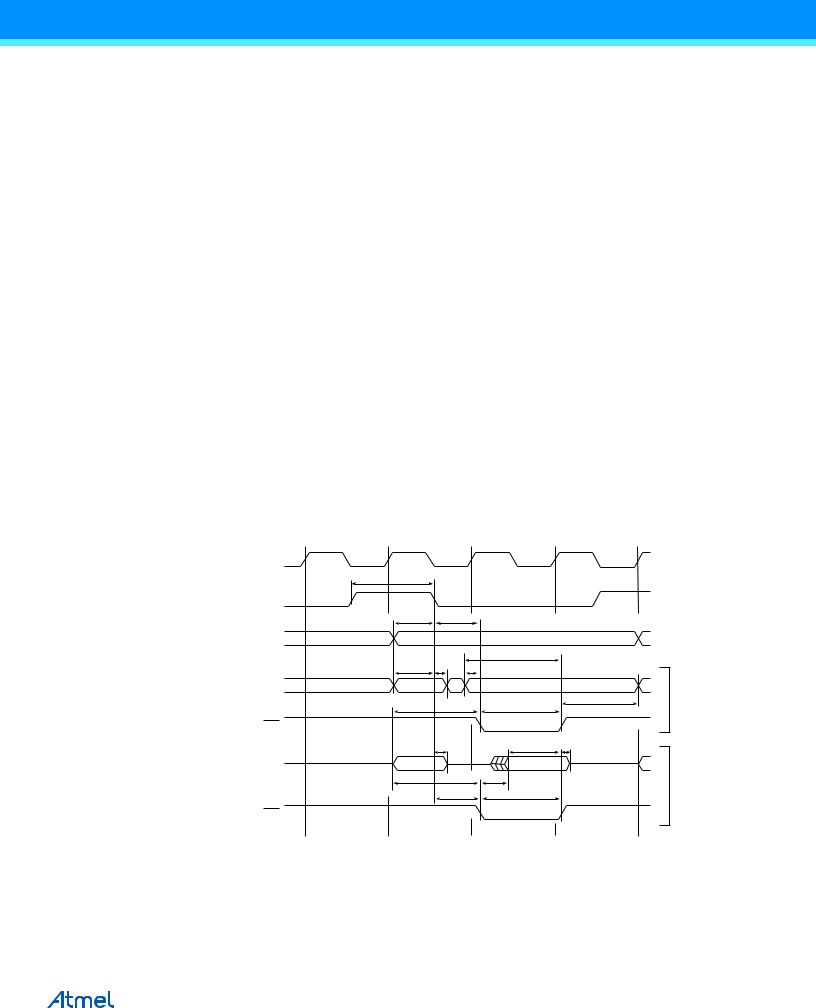
Table 31-17. External Data Memory Characteristics, 2.7 to 5.5 Volts, SRWn1 = 1, SRWn0 = 0
|
|
|
4MHz Oscillator |
Variable Oscillator |
|
||
|
|
|
|
|
|
|
|
|
Symbol |
Parameter |
Min. |
Max. |
Min. |
Max. |
Unit |
|
|
|
|
|
|
|
|
0 |
1/tCLCL |
Oscillator Frequency |
|
|
0.0 |
8 |
MHz |
10 |
tRLDV |
Read Low to Data Valid |
|
690 |
|
3.0tCLCL-60 |
|
12 |
tRLRH |
RD Pulse Width |
735 |
|
3.0tCLCL-15 |
|
ns |
15 |
tDVWH |
Data Valid to WR High |
750 |
|
3.0tCLCL |
|
|
|
|
|
|||||
16 |
tWLWH |
WR Pulse Width |
735 |
|
3.0tCLCL-15 |
|
|
Table 31-18. External Data Memory Characteristics, 2.7 to 5.5 Volts, SRWn1 = 1, SRWn0 = 1
|
|
|
4MHz Oscillator |
Variable Oscillator |
|
||
|
|
|
|
|
|
|
|
|
Symbol |
Parameter |
Min. |
Max. |
Min. |
Max. |
Unit |
|
|
|
|
|
|
|
|
0 |
1/tCLCL |
Oscillator Frequency |
|
|
0.0 |
8 |
MHz |
10 |
tRLDV |
Read Low to Data Valid |
|
690 |
|
3.0tCLCL-60 |
|
12 |
tRLRH |
RD Pulse Width |
735 |
|
3.0tCLCL-15 |
|
|
14 |
tWHDX |
Data Hold After WR High |
485 |
|
2.0tCLCL-15 |
|
ns |
15 |
tDVWH |
Data Valid to WR High |
750 |
|
3.0tCLCL |
|
|
16 |
tWLWH |
WR Pulse Width |
735 |
|
3.0tCLCL-15 |
|
|
Figure 31-9. External Memory Timing (SRWn1 = 0, SRWn0 = 0
|
T1 |
T2 |
|
T3 |
T4 |
System Clock (CLKCPU) |
|
|
|
|
|
|
|
1 |
|
|
|
ALE |
|
|
|
|
|
|
|
4 |
7 |
|
|
A15:8 |
Prev. addr. |
|
|
Address |
|
|
|
|
|
15 |
|
|
|
2 |
3a |
13 |
|
DA7:0 |
Prev. data |
Address |
XX |
Data |
|
|
|
6 |
|
16 |
14 |
|
|
|
|
||
WR |
|
|
|
|
|
|
|
|
3b |
9 |
11 |
DA7:0 (XMBK = 0) |
|
Address |
Data |
|
|
|
|
5 |
|
10 |
|
|
|
|
8 |
12 |
|
RD
Write
Read
ATmega640/V-1280/V-1281/V-2560/V-2561/V [DATASHEET] |
370 |
2549Q–AVR–02/2014
Figure 31-10. External Memory Timing (SRWn1 = 0, SRWn0 = 1)
|
T1 |
T2 |
|
T3 |
T4 |
T5 |
System Clock (CLKCPU) |
|
|
|
|
|
|
|
|
1 |
|
|
|
|
ALE |
|
|
|
|
|
|
|
|
4 |
7 |
|
|
|
A15:8 |
Prev. addr. |
|
|
Address |
|
|
|
|
|
|
|
15 |
|
|
|
2 |
3a |
13 |
|
|
DA7:0 |
Prev. data |
Address |
XX |
|
Data |
|
|
|
6 |
|
|
16 |
14 |
|
|
|
|
|
||
WR |
|
|
|
|
|
|
|
|
|
3b |
|
9 |
11 |
DA7:0 (XMBK = 0) |
|
Address |
|
Data |
|
|
|
|
5 |
|
10 |
|
|
|
|
|
8 |
|
12 |
|
RD
Write
Read
Figure 31-11. External Memory Timing (SRWn1 = 1, SRWn0 = 0)
|
T1 |
T2 |
|
T3 |
T4 |
T5 |
T6 |
System Clock (CLKCPU) |
|
|
|
|
|
|
|
|
|
1 |
|
|
|
|
|
ALE |
|
|
|
|
|
|
|
|
|
4 |
7 |
|
|
|
|
A15:8 |
Prev. addr. |
|
|
|
Address |
|
|
|
|
|
|
|
15 |
|
|
|
|
2 |
3a |
13 |
|
|
|
DA7:0 |
Prev. data |
Address |
XX |
|
Data |
|
|
|
|
6 |
|
|
16 |
|
14 |
|
|
|
|
|
|
||
|
|
|
|
|
|
|
|
WR |
|
|
|
|
|
|
|
|
|
|
3b |
|
9 |
|
11 |
DA7:0 (XMBK = 0) |
|
Address |
|
Data |
|
|
|
|
|
5 |
|
10 |
|
|
|
|
|
|
8 |
|
12 |
|
|
RD
Write
Read
ATmega640/V-1280/V-1281/V-2560/V-2561/V [DATASHEET] |
371 |
2549Q–AVR–02/2014
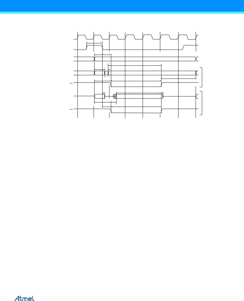
Figure 31-12. External Memory Timing (SRWn1 = 1, SRWn0 = 1)()
|
T1 |
T2 |
|
T3 |
T4 |
T5 |
T6 |
T7 |
System Clock (CLKCPU) |
|
|
|
|
|
|
|
|
|
|
1 |
|
|
|
|
|
|
ALE |
|
|
|
|
|
|
|
|
|
|
4 |
7 |
|
|
|
|
|
A15:8 |
Prev. addr. |
|
|
|
Address |
|
|
|
|
|
|
|
|
15 |
|
|
|
|
|
2 |
3a |
13 |
|
|
|
|
DA7:0 |
Prev. data |
Address |
XX |
|
Data |
|
|
|
|
|
6 |
|
|
16 |
|
|
14 |
|
|
|
|
|
|
|
||
|
|
|
|
|
|
|
|
|
WR |
|
|
|
|
|
|
|
|
|
|
|
3b |
|
9 |
|
11 |
|
DA7:0 (XMBK = 0) |
|
Address |
|
Data |
|
|
|
|
|
|
5 |
|
10 |
|
|
|
|
|
|
|
8 |
|
12 |
|
|
|
RD
Write
Read
The ALE pulse in the last period (T4-T7) is only present if the next instruction accesses the RAM (internal or external).
ATmega640/V-1280/V-1281/V-2560/V-2561/V [DATASHEET] |
372 |
2549Q–AVR–02/2014