


uA7805, uA7808, uA7810 uA7812, uA7815, uA7824
www.ti.com |
SLVS056P –MAY 1976–REVISED JANUARY 2015 |
11 Layout
11.1 Layout Guidelines
Keep trace widths large enough to eliminate problematic I×R voltage drops at the input and output terminals. Input decoupling capacitors should be placed as close to the μA78XX as possible.
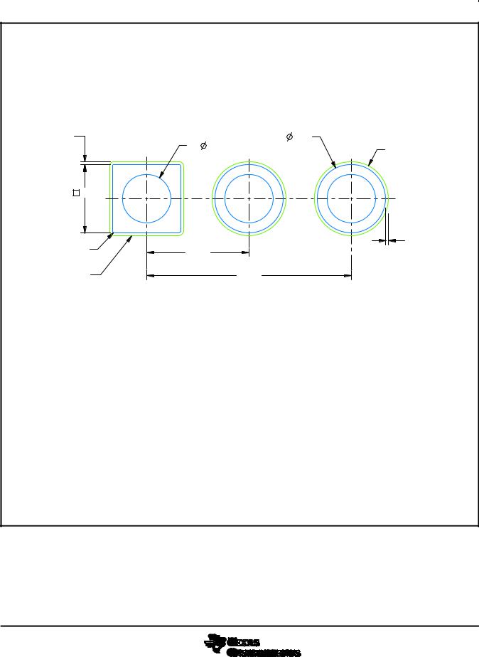
11.2 Layout Example
PF
COMMON
INPUT |
COMMON |
OUTPUT |
PF
|
|
|
|
|
|
|
|
Ground |
|
Ground |
|||||
|
|
|
|
|
|
|
|
|
|
|
|
|
|
|
|
Figure 10. Layout Diagram
12 Device and Documentation Support
12.1 Related Links
The table below lists quick access links. Categories include technical documents, support and community resources, tools and software, and quick access to sample or buy.
Table 1. Related Links
PARTS |
PRODUCT FOLDER |
SAMPLE & BUY |
TECHNICAL |
TOOLS & |
SUPPORT & |
|
DOCUMENTS |
SOFTWARE |
COMMUNITY |
||||
|
|
|
||||
μA7805 |
Click here |
Click here |
Click here |
Click here |
Click here |
|
uA7808 |
Click here |
Click here |
Click here |
Click here |
Click here |
|
uA7810 |
Click here |
Click here |
Click here |
Click here |
Click here |
|
uA7812 |
Click here |
Click here |
Click here |
Click here |
Click here |
|
uA7815 |
Click here |
Click here |
Click here |
Click here |
Click here |
|
uA7924 |
Click here |
Click here |
Click here |
Click here |
Click here |
12.2Trademarks
12.3Electrostatic Discharge Caution
These devices have limited built-in ESD protection. The leads should be shorted together or the device placed in conductive foam during storage or handling to prevent electrostatic damage to the MOS gates.
12.4 Glossary
SLYZ022 — TI Glossary.
This glossary lists and explains terms, acronyms, and definitions.
13 Mechanical, Packaging, and Orderable Information
The following pages include mechanical, packaging, and orderable information. This information is the most current data available for the designated devices. This data is subject to change without notice and revision of this document. For browser-based versions of this data sheet, refer to the left-hand navigation.
Copyright © 1976–2015, Texas Instruments Incorporated |
Submit Documentation Feedback |
15 |
Product Folder Links: uA7805 uA7808 uA7810 uA7812 uA7815 uA7824

PACKAGE OPTION ADDENDUM
www.ti.com |
24-Aug-2018 |
PACKAGING INFORMATION
Orderable Device |
Status |
Package Type |
Package |
Pins |
Package |
Eco Plan |
Lead/Ball Finish |
MSL Peak Temp |
Op Temp (°C) |
Device Marking |
Samples |
|
(1) |
|
Drawing |
|
Qty |
(2) |
(6) |
(3) |
|
(4/5) |
|
UA7805CKCS |
ACTIVE |
TO-220 |
KCS |
3 |
50 |
Pb-Free |
CU SN |
N / A for Pkg Type |
0 to 125 |
UA7805C |
|
|
|
|
|
|
|
(RoHS) |
|
|
|
|
|
UA7805CKCSE3 |
ACTIVE |
TO-220 |
KCS |
3 |
50 |
Pb-Free |
CU SN |
N / A for Pkg Type |
0 to 125 |
UA7805C |
|
|
|
|
|
|
|
(RoHS) |
|
|
|
|
|
UA7805CKCT |
ACTIVE |
TO-220 |
KCT |
3 |
50 |
Pb-Free |
CU SN |
N / A for Pkg Type |
0 to 125 |
UA7805C |
|
|
|
|
|
|
|
(RoHS) |
|
|
|
|
|
UA7805CKTTR |
ACTIVE |
DDPAK/ |
KTT |
3 |
500 |
Green (RoHS |
CU SN |
Level-3-245C-168 HR |
0 to 125 |
UA7805C |
|
|
|
TO-263 |
|
|
|
& no Sb/Br) |
|
|
|
|
|
UA7805CKTTRG3 |
ACTIVE |
DDPAK/ |
KTT |
3 |
500 |
Green (RoHS |
CU SN |
Level-3-245C-168 HR |
0 to 125 |
UA7805C |
|
|
|
TO-263 |
|
|
|
& no Sb/Br) |
|
|
|
|
|
UA7808CKCS |
ACTIVE |
TO-220 |
KCS |
3 |
50 |
Pb-Free |
CU SN |
N / A for Pkg Type |
0 to 125 |
UA7808C |
|
|
|
|
|
|
|
(RoHS) |
|
|
|
|
|
UA7808CKCSE3 |
ACTIVE |
TO-220 |
KCS |
3 |
50 |
Pb-Free |
CU SN |
N / A for Pkg Type |
0 to 125 |
UA7808C |
|
|
|
|
|
|
|
(RoHS) |
|
|
|
|
|
UA7808CKCT |
ACTIVE |
TO-220 |
KCT |
3 |
50 |
Pb-Free |
CU SN |
N / A for Pkg Type |
0 to 125 |
UA7808C |
|
|
|
|
|
|
|
(RoHS) |
|
|
|
|
|
UA7808CKTTR |
ACTIVE |
DDPAK/ |
KTT |
3 |
500 |
Green (RoHS |
CU SN |
Level-3-245C-168 HR |
0 to 125 |
UA7808C |
|
|
|
TO-263 |
|
|
|
& no Sb/Br) |
|
|
|
|
|
UA7810CKCS |
ACTIVE |
TO-220 |
KCS |
3 |
50 |
Pb-Free |
CU SN |
N / A for Pkg Type |
0 to 125 |
UA7810C |
|
|
|
|
|
|
|
(RoHS) |
|
|
|
|
|
UA7810CKCSE3 |
ACTIVE |
TO-220 |
KCS |
3 |
50 |
Pb-Free |
CU SN |
N / A for Pkg Type |
0 to 125 |
UA7810C |
|
|
|
|
|
|
|
(RoHS) |
|
|
|
|
|
UA7810CKTTR |
ACTIVE |
DDPAK/ |
KTT |
3 |
500 |
Green (RoHS |
CU SN |
Level-3-245C-168 HR |
0 to 125 |
UA7810C |
|
|
|
TO-263 |
|
|
|
& no Sb/Br) |
|
|
|
|
|
UA7810CKTTRG3 |
ACTIVE |
DDPAK/ |
KTT |
3 |
500 |
Green (RoHS |
CU SN |
Level-3-245C-168 HR |
0 to 125 |
UA7810C |
|
|
|
TO-263 |
|
|
|
& no Sb/Br) |
|
|
|
|
|
UA7812CKCS |
ACTIVE |
TO-220 |
KCS |
3 |
50 |
Pb-Free |
CU SN |
N / A for Pkg Type |
0 to 125 |
UA7812C |
|
|
|
|
|
|
|
(RoHS) |
|
|
|
|
|
UA7812CKCSE3 |
ACTIVE |
TO-220 |
KCS |
3 |
50 |
Pb-Free |
CU SN |
N / A for Pkg Type |
0 to 125 |
UA7812C |
|
|
|
|
|
|
|
(RoHS) |
|
|
|
|
|
UA7812CKCT |
ACTIVE |
TO-220 |
KCT |
3 |
50 |
Pb-Free |
CU SN |
N / A for Pkg Type |
0 to 125 |
UA7812C |
|
|
|
|
|
|
|
(RoHS) |
|
|
|
|
|
UA7812CKTTR |
ACTIVE |
DDPAK/ |
KTT |
3 |
500 |
Green (RoHS |
CU SN |
Level-3-245C-168 HR |
0 to 125 |
UA7812C |
|
|
|
TO-263 |
|
|
|
& no Sb/Br) |
|
|
|
|
|
Addendum-Page 1

PACKAGE OPTION ADDENDUM
www.ti.com |
|
|
|
|
|
|
|
|
|
24-Aug-2018 |
|
|
|
|
|
|
|
|
|
|
|
|
|
|
|
|
|
|
|
|
|
|
|
|
|
|
|
|
Orderable Device |
Status |
Package Type |
Package |
Pins |
Package |
Eco Plan |
Lead/Ball Finish |
MSL Peak Temp |
Op Temp (°C) |
Device Marking |
|
Samples |
|
(1) |
|
Drawing |
|
Qty |
(2) |
(6) |
(3) |
|
(4/5) |
|
|
UA7812CKTTRG3 |
ACTIVE |
DDPAK/ |
KTT |
3 |
500 |
Green (RoHS |
CU SN |
Level-3-245C-168 HR |
0 to 125 |
UA7812C |
|
|
|
|
TO-263 |
|
|
|
& no Sb/Br) |
|
|
|
|
|
|
UA7815CKCS |
ACTIVE |
TO-220 |
KCS |
3 |
50 |
Pb-Free |
CU SN |
N / A for Pkg Type |
0 to 125 |
UA7815C |
|
|
|
|
|
|
|
|
(RoHS) |
|
|
|
|
|
|
UA7815CKCSE3 |
ACTIVE |
TO-220 |
KCS |
3 |
50 |
Pb-Free |
CU SN |
N / A for Pkg Type |
0 to 125 |
UA7815C |
|
|
|
|
|
|
|
|
(RoHS) |
|
|
|
|
|
|
UA7815CKCT |
ACTIVE |
TO-220 |
KCT |
3 |
50 |
Pb-Free |
CU SN |
N / A for Pkg Type |
0 to 125 |
UA7815C |
|
|
|
|
|
|
|
|
(RoHS) |
|
|
|
|
|
|
UA7815CKTTR |
ACTIVE |
DDPAK/ |
KTT |
3 |
500 |
Green (RoHS |
CU SN |
Level-3-245C-168 HR |
0 to 125 |
UA7815C |
|
|
|
|
TO-263 |
|
|
|
& no Sb/Br) |
|
|
|
|
|
|
UA7824CKCS |
ACTIVE |
TO-220 |
KCS |
3 |
50 |
Pb-Free |
CU SN |
N / A for Pkg Type |
0 to 125 |
UA7824C |
|
|
|
|
|
|
|
|
(RoHS) |
|
|
|
|
|
|
UA7824CKCSE3 |
ACTIVE |
TO-220 |
KCS |
3 |
50 |
Pb-Free |
CU SN |
N / A for Pkg Type |
0 to 125 |
UA7824C |
|
|
|
|
|
|
|
|
(RoHS) |
|
|
|
|
|
|
UA7824CKTTR |
ACTIVE |
DDPAK/ |
KTT |
3 |
500 |
Green (RoHS |
CU SN |
Level-3-245C-168 HR |
0 to 125 |
UA7824C |
|
|
|
|
TO-263 |
|
|
|
& no Sb/Br) |
|
|
|
|
|
|
(1)The marketing status values are defined as follows:
ACTIVE: Product device recommended for new designs.
LIFEBUY: TI has announced that the device will be discontinued, and a lifetime-buy period is in effect.
NRND: Not recommended for new designs. Device is in production to support existing customers, but TI does not recommend using this part in a new design. PREVIEW: Device has been announced but is not in production. Samples may or may not be available.
OBSOLETE: TI has discontinued the production of the device.
(2)RoHS: TI defines "RoHS" to mean semiconductor products that are compliant with the current EU RoHS requirements for all 10 RoHS substances, including the requirement that RoHS substance do not exceed 0.1% by weight in homogeneous materials. Where designed to be soldered at high temperatures, "RoHS" products are suitable for use in specified lead-free processes. TI may reference these types of products as "Pb-Free".
RoHS Exempt: TI defines "RoHS Exempt" to mean products that contain lead but are compliant with EU RoHS pursuant to a specific EU RoHS exemption.
Green: TI defines "Green" to mean the content of Chlorine (Cl) and Bromine (Br) based flame retardants meet JS709B low halogen requirements of <=1000ppm threshold. Antimony trioxide based flame retardants must also meet the <=1000ppm threshold requirement.
(3)MSL, Peak Temp. - The Moisture Sensitivity Level rating according to the JEDEC industry standard classifications, and peak solder temperature.
(4)There may be additional marking, which relates to the logo, the lot trace code information, or the environmental category on the device.
(5)Multiple Device Markings will be inside parentheses. Only one Device Marking contained in parentheses and separated by a "~" will appear on a device. If a line is indented then it is a continuation of the previous line and the two combined represent the entire Device Marking for that device.
Addendum-Page 2

PACKAGE OPTION ADDENDUM
www.ti.com |
24-Aug-2018 |
|
|
(6) Lead/Ball Finish - Orderable Devices may have multiple material finish options. Finish options are separated by a vertical ruled line. Lead/Ball Finish values may wrap to two lines if the finish value exceeds the maximum column width.
Important Information and Disclaimer:The information provided on this page represents TI's knowledge and belief as of the date that it is provided. TI bases its knowledge and belief on information provided by third parties, and makes no representation or warranty as to the accuracy of such information. Efforts are underway to better integrate information from third parties. TI has taken and continues to take reasonable steps to provide representative and accurate information but may not have conducted destructive testing or chemical analysis on incoming materials and chemicals.
TI and TI suppliers consider certain information to be proprietary, and thus CAS numbers and other limited information may not be available for release.
In no event shall TI's liability arising out of such information exceedthe total purchase price of the TI part(s) at issue in this document sold by TI to Customer on an annual basis.
Addendum-Page 3

PACKAGE MATERIALS INFORMATION
www.ti.com |
21-Mar-2017 |
|
|
TAPE AND REEL INFORMATION
*All dimensions are nominal
Device |
Package |
Package |
Pins |
SPQ |
Reel |
Reel |
A0 |
B0 |
K0 |
P1 |
W |
Pin1 |
|
Type |
Drawing |
|
|
Diameter |
Width |
(mm) |
(mm) |
(mm) |
(mm) |
(mm) |
Quadrant |
|
|
|
|
|
(mm) |
W1 (mm) |
|
|
|
|
|
|
UA7805CKTTR |
DDPAK/ |
KTT |
3 |
500 |
330.0 |
24.4 |
10.8 |
16.3 |
5.11 |
16.0 |
24.0 |
Q2 |
|
TO-263 |
|
|
|
|
|
|
|
|
|
|
|
UA7805CKTTR |
DDPAK/ |
KTT |
3 |
500 |
330.0 |
24.4 |
10.8 |
16.1 |
4.9 |
16.0 |
24.0 |
Q2 |
|
TO-263 |
|
|
|
|
|
|
|
|
|
|
|
UA7808CKTTR |
DDPAK/ |
KTT |
3 |
500 |
330.0 |
24.4 |
10.8 |
16.3 |
5.11 |
16.0 |
24.0 |
Q2 |
|
TO-263 |
|
|
|
|
|
|
|
|
|
|
|
UA7810CKTTR |
DDPAK/ |
KTT |
3 |
500 |
330.0 |
24.4 |
10.8 |
16.3 |
5.11 |
16.0 |
24.0 |
Q2 |
|
TO-263 |
|
|
|
|
|
|
|
|
|
|
|
UA7812CKTTR |
DDPAK/ |
KTT |
3 |
500 |
330.0 |
24.4 |
10.8 |
16.3 |
5.11 |
16.0 |
24.0 |
Q2 |
|
TO-263 |
|
|
|
|
|
|
|
|
|
|
|
UA7812CKTTR |
DDPAK/ |
KTT |
3 |
500 |
330.0 |
24.4 |
10.8 |
16.1 |
4.9 |
16.0 |
24.0 |
Q2 |
|
TO-263 |
|
|
|
|
|
|
|
|
|
|
|
UA7815CKTTR |
DDPAK/ |
KTT |
3 |
500 |
330.0 |
24.4 |
10.8 |
16.3 |
5.11 |
16.0 |
24.0 |
Q2 |
|
TO-263 |
|
|
|
|
|
|
|
|
|
|
|
UA7824CKTTR |
DDPAK/ |
KTT |
3 |
500 |
330.0 |
24.4 |
10.8 |
16.3 |
5.11 |
16.0 |
24.0 |
Q2 |
|
TO-263 |
|
|
|
|
|
|
|
|
|
|
|
Pack Materials-Page 1

PACKAGE MATERIALS INFORMATION
www.ti.com |
21-Mar-2017 |
|
|
*All dimensions are nominal
Device |
Package Type |
Package Drawing |
Pins |
SPQ |
Length (mm) |
Width (mm) |
Height (mm) |
|
|
|
|
|
|
|
|
UA7805CKTTR |
DDPAK/TO-263 |
KTT |
3 |
500 |
340.0 |
340.0 |
38.0 |
UA7805CKTTR |
DDPAK/TO-263 |
KTT |
3 |
500 |
350.0 |
334.0 |
47.0 |
|
|
|
|
|
|
|
|
UA7808CKTTR |
DDPAK/TO-263 |
KTT |
3 |
500 |
340.0 |
340.0 |
38.0 |
|
|
|
|
|
|
|
|
UA7810CKTTR |
DDPAK/TO-263 |
KTT |
3 |
500 |
340.0 |
340.0 |
38.0 |
UA7812CKTTR |
DDPAK/TO-263 |
KTT |
3 |
500 |
340.0 |
340.0 |
38.0 |
|
|
|
|
|
|
|
|
UA7812CKTTR |
DDPAK/TO-263 |
KTT |
3 |
500 |
350.0 |
334.0 |
47.0 |
|
|
|
|
|
|
|
|
UA7815CKTTR |
DDPAK/TO-263 |
KTT |
3 |
500 |
340.0 |
340.0 |
38.0 |
UA7824CKTTR |
DDPAK/TO-263 |
KTT |
3 |
500 |
340.0 |
340.0 |
38.0 |
|
|
|
|
|
|
|
|
Pack Materials-Page 2


|
PACKAGE OUTLINE |
KCT0003A |
TO-220 - 20.55 mm max height |
SCALE 0.850
|
|
|
|
|
|
|
TO-220 |
|
|
|
|
4.65 |
|
OPTIONAL |
|
|
|
|
10.67 |
4.25 |
0.61 |
2X |
|
|
|
|
3.05 |
8.74 |
|
||
|
|
|
9.65 |
0.46 |
|
||
|
|
|
2.54 |
8.14 |
|
||
|
|
|
|
|
|
||
6.86 |
|
|
|
|
(6.35) |
|
|
5.84 |
|
|
|
|
|
|
|
|
|
|
|
|
|
|
|
|
|
|
|
3.60-3.96 |
|
|
12.8 |
|
|
|
|
|
|
|
12.2 |
8.79 |
|
|
|
20.55 |
OPTIONAL |
|
|
|
|
|
MAX |
|
|
||
8.39 |
|
|
|
CHAMFER |
|
|
|
|
|
|
|
|
|
||
(3.18) |
|
4.04 MAX |
|
|
|
||
NOTE 3 |
|
|
|
|
|||
14.73 |
|
|
|
OPTIONAL |
|
|
|
|
|
|
|
|
|
|
|
12.70 |
|
|
|
|
|
|
|
|
|
1 |
3 |
|
|
|
|
3X |
0.91 |
|
0.61 |
|
|
|
|
0.71 |
|
0.46 |
2.92 |
|
|
||
|
|
|
2X |
2.54 |
|
|
|
|
|
|
2.03 |
|
|
||
|
1.78 |
|
|
|
|
||
3X |
|
|
|
|
|
||
|
1.14 |
|
|
|
|
|
|
|
|
|
5.08 |
|
|
|
|
|
|
|
|
|
|
4223034/B |
08/2018 |
NOTES:
1. Dimensions are in millimeters. Any dimension in brackets or parenthesis are for reference only. Dimensioning and tolerancing per ASME Y14.5M.
2. This drawing is subject to change without notice.
3. Lead dimensions are not controlled within this area.
4. Reference JEDEC registration TO-220.
www.ti.com

|
EXAMPLE BOARD LAYOUT |
KCT0003A |
TO-220 - 20.55 mm max height |
|
TO-220 |
0.07 MAX |
|
METAL |
|
|
|
|
|
|
|
|
|
ALL AROUND |
|
3X ( 1.3) |
2X ( |
1.8) |
2X SOLDER MASK |
|
|
VIA |
METAL |
OPENING |
|
( |
1.8) |
|
|
|
|
|
|
1 |
2 |
3 |
2X 0.07 MAX |
(R 0.05) |
ALL AROUND |
||||
(2.54) |
|
|
|
||
|
|
|
|
|
|
SOLDER MASK |
|
(5.08) |
|
|
|
OPENING |
|
|
|
||
|
|
|
|
||
|
|
LAND PATTERN EXAMPLE |
|
||
|
|
NON-SOLDER MASK DEFINED |
|
||
|
|
|
SCALE:15X |
|
|
4223034/B 08/2018
www.ti.com

|
|
PACKAGE OUTLINE |
KCS0003B |
|
TO-220 - 19.65 mm max height |
|
SCALE 0.850 |
|
|
|
TO-220 |
|
|
4.7 |
|
|
10.36 |
|
4.4 |
|
|
2.9 |
1.32 |
8.55 |
||
9.96 |
1.22 |
|||
2.6 |
8.15 |
|||
|
|
|||
6.5 |
|
|
(6.3) |
|
6.1 |
|
|
||
|
|
|
||
( |
3.84) |
|
12.5 |
|
|
|
|
12.1 |
|
9.25 |
19.65 MAX |
|
|
|
|
|
|
||
9.05 |
|
|
|
|
|
|
|
3X |
|
|
|
|
|
3.9 MAX |
|
13.12 |
|
|
|
||
12.70 |
|
|
|
||
|
|
1 |
3 |
|
|
3X |
0.90 |
|
|
0.47 |
|
0.77 |
|
|
0.34 |
||
|
|
|
2X |
2.54 |
2.79 |
|
|
|
2.59 |
||
|
1.36 |
|
|
||
3X |
|
|
|
||
|
1.23 |
|
|
|
|
|
|
|
5.08 |
|
|
4222214/B 08/2018
NOTES:
1.Dimensions are in millimeters. Any dimension in brackets or parenthesis are for reference only. Dimensioning and tolerancing per ASME Y14.5M.
2.This drawing is subject to change without notice.
3.Reference JEDEC registration TO-220.
www.ti.com
|
EXAMPLE BOARD LAYOUT |
KCS0003B |
TO-220 - 19.65 mm max height |
|
TO-220 |
0.07 MAX |
|
2X (1.7) |
|
ALL AROUND |
3X (1.2) |
METAL |
2X SOLDER MASK |
|
|
|
|
|
|
|
OPENING |
(1.7) |
|
|
|
1 |
2 |
3 |
0.07 MAX |
R (0.05) |
(2.54) |
|
ALL AROUND |
|
|
|
|
SOLDER MASK |
(5.08) |
|
|
OPENING |
|
|
|
|
LAND PATTERN EXAMPLE |
|
|
|
NON-SOLDER MASK DEFINED |
|
|
|
SCALE:15X |
|
|
4222214/B 08/2018
www.ti.com
IMPORTANT NOTICE AND DISCLAIMER
TI PROVIDES TECHNICAL AND RELIABILITY DATA (INCLUDING DATASHEETS), DESIGN RESOURCES (INCLUDING REFERENCE DESIGNS), APPLICATION OR OTHER DESIGN ADVICE, WEB TOOLS, SAFETY INFORMATION, AND OTHER RESOURCES “AS IS” AND WITH ALL FAULTS, AND DISCLAIMS ALL WARRANTIES, EXPRESS AND IMPLIED, INCLUDING WITHOUT LIMITATION ANY IMPLIED WARRANTIES OF MERCHANTABILITY, FITNESS FOR A PARTICULAR PURPOSE OR NON-INFRINGEMENT OF THIRD PARTY INTELLECTUAL PROPERTY RIGHTS.
These resources are intended for skilled developers designing with TI products. You are solely responsible for (1) selecting the appropriate TI products for your application, (2) designing, validating and testing your application, and (3) ensuring your application meets applicable standards, and any other safety, security, or other requirements. These resources are subject to change without notice. TI grants you permission to use these resources only for development of an application that uses the TI products described in the resource. Other reproduction and display of these resources is prohibited. No license is granted to any other TI intellectual property right or to any third party intellectual property right. TI disclaims responsibility for, and you will fully indemnify TI and its representatives against, any claims, damages, costs, losses, and liabilities arising out of your use of these resources.
TI’s products are provided subject to TI’s Terms of Sale (www.ti.com/legal/termsofsale.html) or other applicable terms available either on ti.com or provided in conjunction with such TI products. TI’s provision of these resources does not expand or otherwise alter TI’s applicable warranties or warranty disclaimers for TI products.
Mailing Address: Texas Instruments, Post Office Box 655303, Dallas, Texas 75265
Copyright © 2019, Texas Instruments Incorporated