

Стабилизатор / AK4493EQ_EVB
.pdf[AKD4493-A]
AKD4493-A
AK4493 Evaluation Board Rev.1
1. General Description
The AKD4493-A is an evaluation board for the AK4493 (Premium 32-bit 2ch DAC). It integrates differential output low pass filters, allowing quick evaluation with digital audio interface.
■ Ordering Guide
AKD4493-A -- Evaluation Board for the AK4493
(Control software is included in this package.)
2. Function
10-pin Header for Serial Control
Low Pass Filters (LPF) for Pre-amplifier Outputs
Digital Audio Interface (AK4115)
DIR
COAX In |
Lch |
|
AK4115 |
||
|
||
Opt In |
|
|
AK4493 |
2nd Order LPF |
|
PORT2 |
Rch |
Figure 1. AKD4493-A Block Diagram (Note 1)
Note 1. Circuit schematics are attached at the end of this document.
<KM125201> |
2017/07 |
|
- 1 - |
[AKD4493-A]
3. Table of Contents |
|
1.General Description................................................................................................................................................ |
1 |
■ Ordering Guide .......................................................................................................................................................... |
1 |
2.Function.................................................................................................................................................................. |
1 |
3.Table of Contents ................................................................................................................................................... |
2 |
4.Evaluation Board .................................................................................................................................................... |
3 |
■ Board Diagram........................................................................................................................................................... |
3 |
■ Description................................................................................................................................................................. |
3 |
5.Operation Sequence................................................................................................................................................ |
5 |
■ Power Supply Line Settings ....................................................................................................................................... |
5 |
■ Evaluation Mode........................................................................................................................................................ |
7 |
■ Jumper Pin and DIP Switch Settings ......................................................................................................................... |
8 |
■ Digital Filter Mode setting in parallel control mode................................................................................................ |
11 |
■ Power-up.................................................................................................................................................................. |
11 |
■ Serial Control Mode ................................................................................................................................................ |
12 |
6.Control Software Manual ..................................................................................................................................... |
14 |
■ Evaluation Board and Control Software Settings..................................................................................................... |
14 |
■ Operation Overviews ............................................................................................................................................... |
15 |
■ Tab Functions .......................................................................................................................................................... |
16 |
■ Dialog Boxes ........................................................................................................................................................... |
18 |
7.Revision History................................................................................................................................................... |
22 |
IMPORTANT NOTICE ....................................................................................................................................... |
23 |
<KM125201> |
2017/07 |
|
- 2 - |
[AKD4493-A]
4. Evaluation Board
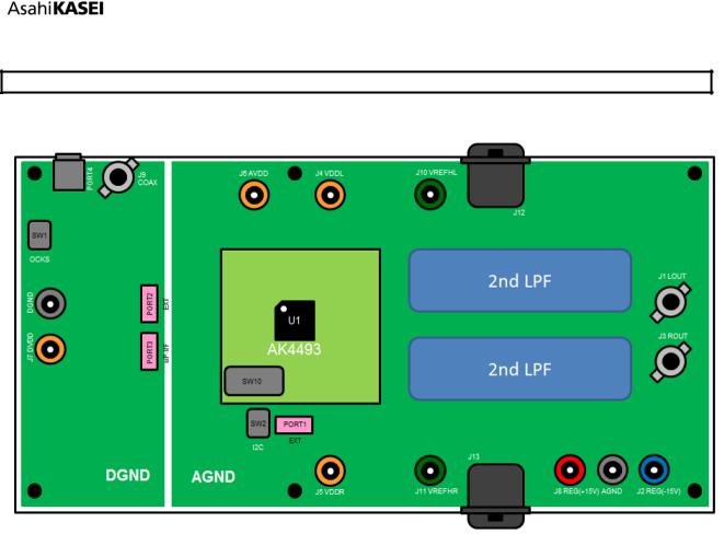
■ Board Diagram
Figure 2. AKD4493-A board diagram
■ Description
(1) Connectors for Power Supply and GND
(REG(+15V), REG(-15V), AVDD, DVDD, VDDL, VDDR, VREFHL, VREFHR, AGND, DGND) Connectors for power supply and the ground
Refer to the “■ Power Supply Line Settings” for details.
(2)SPDIF Input Connectors (J9/BNC Connector, PORT4/Optical Connector) Input a SPDIF signal to the AK4115.
Set the JP9 jumper pin to “BNC” side when using the J9 (BNC Connector) jack. Set the JP9 jumper pin to “OPT” side when using the PORT4 (Optical Connector).
(3)Analog Output Terminals (J1 / J3, BNC Connector)
Single-ended Analog Output Connector
(4)Analog Differential Output Terminals (J12 / J13, XLR Connector) Differential Analog Output Connector
<KM125201> |
2017/07 |
|
- 3 - |

[AKD4493-A]
(5) EXT PORT (PORT2)
10-pin Header for External Interfacing
External digital audio devices are interfaced to this port.
Set the JP5, JP6, JP7 and JP8 jumper pins to “EXT” side when using the PORT2 (EXT).
|
|
Pin |
I/O |
Function |
pin |
I/O |
Function |
|
|
1 |
I |
MCLK |
2 |
P |
GND |
|
|
3 |
I |
BICK |
4 |
P |
GND |
|
|
5 |
I |
SDTO |
6 |
P |
GND |
|
|
7 |
I |
LRCK |
8 |
P |
GND |
|
|
9 |
I |
|
10 |
P |
GND |
|
|
|
|
Table 1. PORT2 (EXT) Pin Assignments |
|||
(6) |
AK4115 (U7) |
|
|
|
|
|
|
|
The AK4115 is a digital audio transceiver. |
|
|
|
|||
|
It is used when evaluating sound quality of the AK4493 by SPDIF signals. |
||||||
(7) µP-IF PORT (PORT3)
10-pin Header for the USB I/F board
Connect the USB I/F board for IBM-AT compatible computers to this port for a connection to a USB port of a PC. Refer to the “■ Serial Control Mode” for details.
(8) Slide Switches (SW1 / SW2 / SW10)
Setting switches for the AK4493 and the AK4115. Upside is “H” (ON) and Downside is “L” (OFF).
Refer to “■ Jumper Pin and DIP Switch Settings” for details.
<KM125201> |
2017/07 |
|
- 4 - |
[AKD4493-A]
5. Operation Sequence
■ Power Supply Line Settings
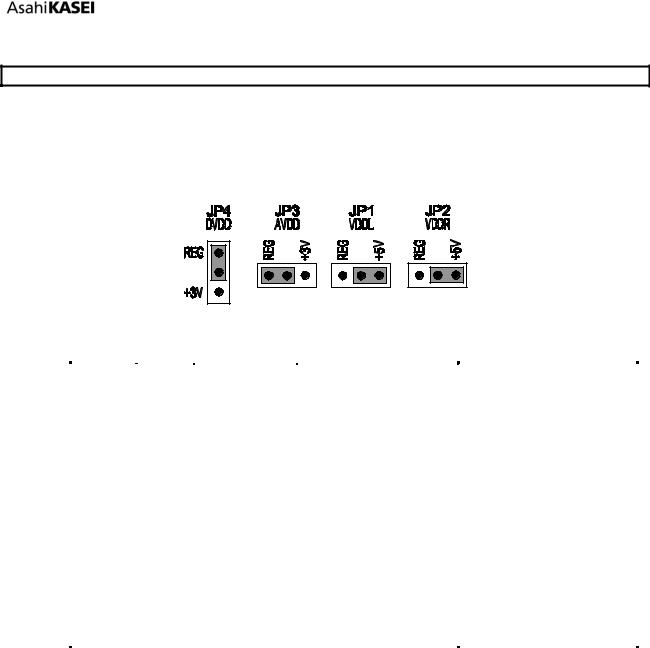
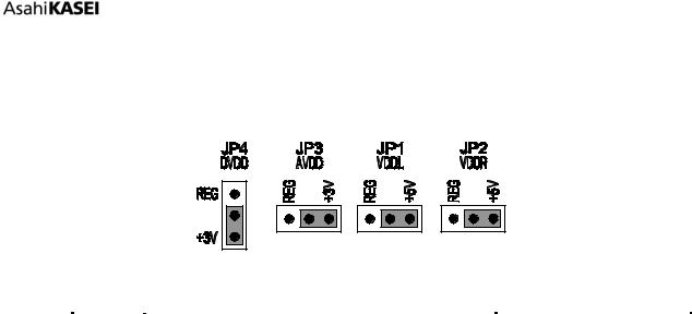
(1)In case of using the regulators;
For the DVDD and AVDD power supply lines. < Default >
Set up the jumper pins.
|
|
|
|
Figure 3. jumper pins setting |
|
|
Set up the power supply lines. |
|
|
|
|||
|
Name |
Color |
|
Voltage |
Content |
Note |
|
REG |
Red |
|
+10 +15V |
For regulators, and plus |
Must be connected. |
|
(+15V) |
|
|
[Typ: +15V] |
power supply of the op-amp |
|
|
REG |
Blue |
|
-10 -15V |
Minus power supply of the |
Must be connected. |
|
(-15V) |
|
|
[Typ: -15V] |
op-amp |
|
|
VREFHL |
Green |
|
+10 +15V |
For regulators. |
Must be connected. |
|
|
|
|
[Typ: +15V] |
VREFHL of AK4493 |
|
|
VREFHR |
Green |
|
+10 +15V |
For regulators. |
Must be connected. |
|
|
|
|
[Typ: +15V] |
VREFHR of AK4493 |
|
|
DVDD |
Orange |
|
Open |
DVDD of AK4493 |
Must be “Open”. |
|
AVDD |
Orange |
|
Open |
AVDD of AK4493 |
Must be “Open”. |
|
VDDL |
Orange |
+4.75 +5.25V |
VDDL of AK4493 |
Must be connected. |
|
|
|
|
|
[Typ: +5V] |
|
|
|
VDDR |
Orange |
+4.75 +5.25V |
VDDR of AK4493 |
Must be connected. |
|
|
|
|
|
[Typ: +5V] |
|
|
|
AGND |
Black |
|
0V |
Analog ground |
Must be connected. |
|
DGND |
Black |
|
0V |
Digital ground |
Must be connected. |
|
|
|
|
Table 2. Connection of the power supply. (Note 2) |
||
Note 2. Each power supply line should be distributed separately from the power supply unit.
<KM125201> |
2017/07 |
|
- 5 - |
[AKD4493-A]
(2) In case of using the power supply connectors;
For the DVDD, AVDD, VDDL and VDDR power supply lines.
Set up the jumper pins.
|
|
|
|
Figure 4. jumper pins setting |
|
|
|
||
Set up the power supply lines. |
|
|
|
|
|
||||
|
Name |
Color |
|
Voltage |
|
Content |
|
Note |
|
|
|
|
|
|
|||||
|
REG |
Red |
|
+10 +15V |
|
For regulators, and plus |
|
Must be connected. |
|
|
(+15V) |
|
|
[Typ: +15V] |
|
power supply of the op-amp |
|
|
|
|
REG |
Blue |
|
-10 -15V |
|
Minus power supply of the |
|
Must be connected. |
|
|
(-15V) |
|
|
[Typ: -15V] |
|
op-amp |
|
|
|
|
VREFHL |
Green |
|
+10 +15V |
|
For regulators. |
|
Must be connected. |
|
|
|
|
|
[Typ: +15V] |
|
VREFHL of AK4493 |
|
|
|
|
VREFHR |
Green |
|
+10 +15V |
|
For regulators. |
|
Must be connected. |
|
|
|
|
|
[Typ: +15V] |
|
VREFHR of AK4493 |
|
|
|
|
DVDD |
Orange |
|
+2.7 +3.6V |
|
DVDD of AK4493 |
|
Must be connected. |
|
|
|
|
|
[Typ: +3.3V] |
|
|
|
|
|
|
AVDD |
Orange |
|
+2.7 +3.6V |
|
AVDD of AK4493 |
|
Must be connected. |
|
|
|
|
|
[Typ: +3.3V] |
|
|
|
|
|
|
VDDL |
Orange |
|
+4.75 +5.25V |
|
VDDL of AK4493 |
|
Must be connected. |
|
|
|
|
|
[Typ: +5V] |
|
|
|
|
|
|
VDDR |
Orange |
|
+4.75 +5.25V |
|
VDDR of AK4493 |
|
Must be connected. |
|
|
|
|
|
[Typ: +5V] |
|
|
|
|
|
|
AGND |
Black |
|
0V |
|
Analog ground |
|
Must be connected. |
|
|
DGND |
Black |
|
0V |
|
Digital ground |
|
Must be connected. |
|
Table 3. Connection of the power supply. (Note 2)
<KM125201> |
2017/07 |
|
- 6 - |
[AKD4493-A]
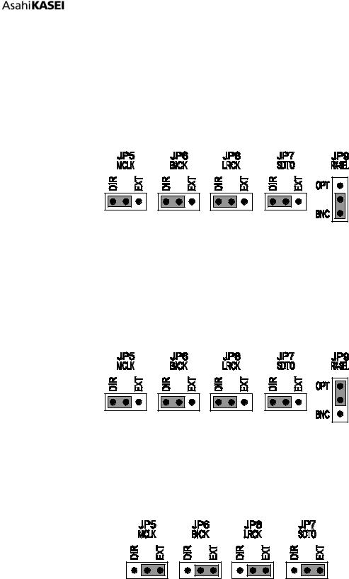
■ Evaluation Mode
(1) Evaluation with a DIR (COAX) < Default >
The J9 (COAX) jack is used in this mode. The DIR (AK4115) generates MCLK, BICK, LRCK and SDATA from the input data of the J9 (COAX) connector.
Set the JP9 (RX-SEL) jumper pin to “BNC”, and set the JP5 (MCLK), JP6 (BICK), JP8 (LRCK) and JP7 (SDTO) jumper pins to “DIR”.
Set up the jumper pins.
Figure 5. Jumper Pin Settings with DIR
(2) Evaluation with a DIR (OPTICAL)
The PORT4 (OPTICAL) is used in this mode. The DIR (AK4115) generates MCLK, BICK, LRCK and SDATA from the input data of the PORT4 (OPTICAL) connector.
Set the JP9 jumper pin to “OPT”, and set the JP5 (MCLK), JP6 (BICK), JP8 (LRCK) and JP7 (SDTO) jumper pins to “DIR”.
Set up the jumper pins.
Figure 6. Jumper Pin Settings with DIR
(3) In the case that all interface clocks including the master clock are inputs externally (PORT )
Input all interface clocks including the master clock to the PORT2 (EXT).
Set JP5 (MCLK), JP6 (BICK), JP8 (LRCK) and JP7 (SDTO) jumper pins to “EXT”.
Set up the jumper pins.
Figure 7. Jumper Pin Settings with External Clocks
<KM125201> |
2017/07 |
|
- 7 - |

[AKD4493-A]
■Jumper Pin and DIP Switch Settings
(1)Jumper Pin Settings
Sub Board
[JP10 (PS1)]: SMUTE/CSN pin input select SMUTE: This setting is for Parallel Control Mode.
CSN: This setting is for Serial Control Mode. < Default >
[JP11 (PS2)]: SD/CCLK/SCL pin input select SD: This setting is for Parallel Control Mode.
CCLK/SCL: This setting is for Serial Control Mode. < Default >
[JP12 (PS3)]: SLOW/CDTI/SDA pin input select SLOW: This setting is for Parallel Control Mode.
CDTI/SDA: This setting is for Serial Control Mode. < Default >
[JP13 (PS4)]: SSLOW/WCK pin input select
H: The SSLOW pin is set to “H” in Parallel Control Mode.
L: The SSLOW pin is set to “L” in Parallel Control Mode. < Default >
OPEN: It can be an input pin header for a WCK signal when the AK4493 is in Serial Control Mode and the external digital filter I/F is used.
[JP14 (DZFL)]: DIF0/DZFL pin connection select SHORT: This setting is for Parallel Control Mode.
OPEN: This setting is for Serial Control Mode. < Default >
[JP15 (DZFR)]: DIF1/DZFR pin connection select SHORT: This setting is for Parallel Control Mode.
OPEN: This setting is for Serial Control Mode. < Default >
<KM125201> |
2017/07 |
|
- 8 - |

[AKD4493-A]
(2) DIP Switch Setting
Upside is ON (“H”), and Downside is OFF (“L”).
Main Board
[SW1]: Setting of the AK4115 |
|
|
|
|||
|
No. |
Name |
|
ON (“H”) |
OFF (“L”) |
Default |
|
1 |
OCKS1 |
|
Master Clock setting for AK4115 |
H |
|
|
2 |
OCKS0 |
|
Refer to Table 7 |
L |
|
|
|
|
|
Table 4. SW1 Setting |
|
|
[SW2]: Setting of the AK4493-1 |
|
|
||||
|
No. |
Name |
|
ON (“H”) |
OFF (“L”) |
Default |
|
1 |
TESTE |
|
Test Mode |
Normal Mode |
L |
|
2 |
I2C |
|
I2C-Bus |
3-wire |
L |
|
(Note 3) |
|
Control Mode |
Serial Control Mode |
||
|
|
|
|
|||
Table 5. SW2 Setting
Note 3. The I2C pin is valid when SW10 (7 pin/PSN) is set to “L” (Serial Control Mode).
Sub Board
[SW10]: Setting of the AK4493-2 |
|
|
|
||||||||
|
No. |
Name |
|
ON (“H”) |
|
|
|
OFF (“L”) |
Default |
|
|
|
|
|
|
||||||||
|
1 |
SMUTE |
|
Mute “ON” |
|
|
|
Mute “OFF” |
L |
|
|
|
2 |
SD |
|
Digital Filter Setting |
H |
|
|||||
|
3 |
SLOW |
|
Refer to Table 8 |
L |
|
|||||
|
4 |
DIF0 |
|
Audio I/F Format for AK4493 |
L |
|
|||||
|
|
|
|
|
|
||||||
|
5 |
DIF1 |
|
H |
|
||||||
|
|
Refer to Table 9 |
|
||||||||
|
6 |
DIF2 |
|
L |
|
||||||
|
|
|
|
|
|
|
|
|
|||
|
/CAD0 |
|
CAD0 pin= “H” |
|
|
|
CAD0 pin= “L” |
|
|||
|
|
|
|
|
|
|
|
||||
|
7 |
PSN |
|
Parallel Control Mode |
|
|
|
Serial Control Mode |
L |
|
|
|
8 |
DEM0 |
|
De-emphasis Control |
|
|
|
Refer to Table 10 |
H |
|
|
|
|
( Pararell Control Mode ) |
|
||||||||
|
|
|
|
|
|
||||||
|
9 |
LDOE |
|
LDO “ON” |
|
|
LDO “OFF” |
H |
|
||
|
10 |
ACKS |
|
Auto Setting Mode |
|
|
|
|
Manual Setting Mode |
L |
|
|
/CAD1 |
|
CAD1 pin= “H” |
|
|
|
CAD1 pin= “L” |
|
|||
|
|
|
|
|
|
|
|||||
Table 6. SW10 Setting
<KM125201> |
2017/07 |
|
- 9 - |

[AKD4493-A]
|
Mode |
|
|
OCKS1 |
|
OCKS0 |
|
MCKO1 |
|
|
fs (max) |
|
|||||
0 |
|
|
|
L |
|
L |
|
256fs |
|
|
96 kHz |
|
|||||
1 |
|
|
|
L |
|
H |
|
256fs |
|
|
96 kHz |
< Default > |
|||||
2 |
|
|
|
H |
|
L |
|
512fs |
|
|
48 kHz |
||||||
3 |
|
|
|
H |
|
H |
|
128fs |
|
|
192 kHz |
|
|||||
|
|
|
|
|
Table 7. |
Master Clock Setting |
|
|
|
|
|
||||||
|
|
|
|
|
|
|
|
|
|
|
|
|
|
|
|
|
|
|
SD |
|
|
|
SLOW |
|
|
|
|
Mode |
|
|
|
|
|
||
|
L |
|
|
|
|
L |
Sharp roll-off filter |
|
|
|
|
|
|||||
|
L |
|
|
|
|
H |
Slow roll-off filter |
|
|
< Default > |
|
||||||
|
H |
|
|
|
|
L |
Short delay sharp roll-off filter |
|
|
|
|||||||
|
H |
|
|
|
|
H |
Short delay slow roll-off filter |
|
|
|
|
|
|||||
|
|
|
|
|
Table 8. |
Digital Filter Setting |
|
|
|
|
|
||||||
|
|
|
|
|
|
|
|
|
|
|
|
|
|
|
|
|
|
|
Mode |
|
DIF2 |
|
|
DIF1 |
|
DIF0 |
|
|
Input Format |
|
BICK |
|
|
||
|
|
pin |
|
|
pin |
|
pin |
|
|
|
|
|
|
|
|||
|
|
|
|
|
|
|
|
|
|
|
|
|
|
||||
0 |
|
|
L |
|
|
L |
|
L |
|
16bit LSB justified |
|
32fs |
|
|
|||
1 |
|
|
L |
|
|
L |
|
H |
|
20bit LSB justified |
|
48fs |
< Default > |
||||
|
2 |
|
|
L |
|
|
H |
|
L |
|
24bit MSB justified |
|
48fs |
||||
3 |
|
|
L |
|
|
H |
|
H |
|
24bit I2S Compatible |
|
48fs |
|
|
|||
4 |
|
H |
|
|
L |
|
L |
|
24bit LSB justified |
|
48fs |
|
|
||||
5 |
|
H |
|
|
L |
|
H |
|
32bit LSB justified |
|
64fs |
|
|
||||
6 |
|
H |
|
|
H |
|
L |
|
32bit MSB justified |
|
64fs |
|
|
||||
7 |
|
H |
|
|
H |
|
H |
|
32bit I2 Compatible |
|
64fs |
|
|
||||
|
|
|
|
|
|
Table 9. |
AK4414 |
Audio I/F Format |
|
|
|
|
|
||||
|
|
|
|
|
|
|
|
|
|
|
|
|
|
|
|
||
|
DEM0 |
|
|
|
Mode |
|
|
|
|
|
|
|
|
|
|
||
|
L |
|
|
44.1kHz |
|
< Default > |
|
|
|
|
|
||||||
|
H |
|
|
|
OFF |
|
|
|
|
|
|
||||||
Table 10. AK4493 De-emphasis Control
<KM125201> |
2017/07 |
|
- 10 - |