

схемы для компов БП / PC-POWER / TL594
.pdfPrecision Switchmode
Pulse Width Modulation
Control Circuit
The TL594 is a fixed frequency, pulse width modulation control circuit designed primarily for Switchmode power supply control.
•Complete Pulse Width Modulation Control Circuitry
•On±Chip Oscillator with Master or Slave Operation
•On±Chip Error Amplifiers
•On±Chip 5.0 V Reference, 1.5% Accuracy
•Adjustable Deadtime Control
•Uncommitted Output Transistors Rated to 500 mA Source or Sink
•Output Control for Push±Pull or Single±Ended Operation
•Undervoltage Lockout
Order this document by TL594/D
TL594
PRECISION SWITCHMODE PULSE WIDTH MODULATION CONTROL CIRCUIT
SEMICONDUCTOR
TECHNICAL DATA
D SUFFIX
PLASTIC PACKAGE
CASE 751B
(SO±16)
N SUFFIX
PLASTIC PACKAGE
CASE 648
MAXIMUM RATINGS (Full operating ambient temperature range applies, unless otherwise noted.)
Rating |
Symbol |
Value |
Unit |
|
|
|
|
Power Supply Voltage |
VCC |
42 |
V |
Collector Output Voltage |
VC1, |
42 |
V |
|
VC2 |
|
|
Collector Output Current |
IC1, IC2 |
500 |
mA |
(each transistor) (Note 1) |
|
|
|
|
|
|
|
Amplifier Input Voltage Range |
VIR |
±0.3 to +42 |
V |
Power Dissipation @ TA ≤ 45°C |
PD |
1000 |
mW |
Thermal Resistance, |
RθJA |
80 |
°C/W |
Junction±to±Ambient |
|
|
|
|
|
|
|
Operating Junction Temperature |
TJ |
125 |
°C |
Storage Temperature Range |
Tstg |
±55 to +125 |
°C |
Operating Ambient Temperature Range |
TA |
|
°C |
TL594ID, CN |
|
0 to +70 |
|
TL594CD, IN |
|
±25 to +85 |
|
|
|
|
|
Derating Ambient Temperature |
TA |
45 |
°C |
NOTES: 1. Maximum thermal limits must be observed.
PIN CONNECTIONS
Noninv |
1 |
+ |
|
|
+ |
16 |
Noninv |
Input |
1 |
2 |
Input |
||||
Inv |
|
Error |
Error |
|
Inv |
||
|
Amp |
|
|
Amp |
|
||
Input |
2 |
± |
|
VCC |
± |
15 |
Input |
|
|
|
|||||
Compen/PWN |
3 |
|
|
|
5.0 V |
14 |
V |
Comp Input |
|
≈ 0.1 V |
|
|
REF |
|
ref |
Deadtime |
|
|
|
|
|
Output |
|
4 |
|
|
|
|
13 |
||
Control |
|
|
|
|
Control |
||
CT |
5 |
Oscillator |
|
|
12 |
VCC |
|
|
|
|
|
|
|
||
RT |
6 |
|
|
|
Q2 |
11 |
C2 |
Ground |
7 |
|
|
|
|
10 |
E2 |
C1 |
8 |
|
Q1 |
|
|
9 |
E1 |
|
|
|
|
||||
(Top View)
ORDERING INFORMATION
|
Operating |
|
|
Device |
Temperature Range |
Package |
|
|
|
|
|
TL594CD |
TA = 0° to +70°C |
SO±16 |
|
|
|
||
TL594CN |
Plastic |
||
|
|||
|
|
|
|
TL594IN |
TA = ± 25° to +85°C |
Plastic |
Motorola, Inc. 1996 |
Rev 0 |

TL594
RECOMMENDED OPERATING CONDITIONS
Characteristics |
Symbol |
Min |
Typ |
Max |
Unit |
|
|
|
|
|
|
Power Supply Voltage |
VCC |
7.0 |
15 |
40 |
V |
Collector Output Voltage |
VC1, VC2 |
± |
30 |
40 |
V |
Collector Output Current (Each transistor) |
IC1, IC2 |
± |
± |
200 |
mA |
Amplified Input Voltage |
Vin |
0.3 |
± |
VCC ± 2.0 |
V |
Current Into Feedback Terminal |
lfb |
± |
± |
0.3 |
mA |
Reference Output Current |
lref |
± |
± |
10 |
mA |
Timing Resistor |
RT |
1.8 |
30 |
500 |
kΩ |
Timing Capacitor |
CT |
0.0047 |
0.001 |
10 |
μF |
Oscillator Frequency |
fosc |
1.0 |
40 |
200 |
kHz |
PWM Input Voltage (Pins 3, 4, 13) |
± |
0.3 |
± |
5.3 |
V |
|
|
|
|
|
|
ELECTRICAL CHARACTERISTICS (VCC = 15 V, CT = 0.01 μF, RT = 12 kΩ, unless otherwise noted.)
For typical values TA = 25°C, for min/max values TA is the operating ambient temperature range that applies, unless otherwise noted.
Characteristics |
Symbol |
Min |
|
Typ |
|
Max |
Unit |
|
|
|
|
|
|
|
|
REFERENCE SECTION |
|
|
|
|
|
|
|
|
|
|
|
|
|
|
|
Reference Voltage |
Vref |
|
|
|
|
|
V |
(IO = 1.0 mA, TA = 25°C) |
|
4.925 |
|
5.0 |
|
5.075 |
|
(IO = 1.0 mA) |
|
4.9 |
|
± |
|
5.1 |
|
Line Regulation (VCC = 7.0 V to 40 V) |
Regline |
± |
|
2.0 |
|
25 |
mV |
Load Regulation (IO = 1.0 mA to 10 mA) |
Regload |
± |
|
2.0 |
|
15 |
mV |
Short Circuit Output Current (Vref = 0 V) |
ISC |
15 |
|
40 |
|
75 |
mA |
OUTPUT SECTION |
|
|
|
|
|
|
|
|
|
|
|
|
|
|
|
Collector Off±State Current (VCC = 40 V, VCE = 40 V) |
IC(off) |
± |
|
2.0 |
|
100 |
μA |
Emitter Off±State Current (VCC = 40 V, VC = 40 V, VE = 0 V) |
IE(off) |
± |
|
± |
|
±100 |
μA |
Collector±Emitter Saturation Voltage (Note 2) |
|
|
|
|
|
|
V |
Common±Emitter (VE = 0 V, IC = 200 mA) |
VSAT(C) |
± |
|
1.1 |
|
1.3 |
|
Emitter±Follower (VC = 15 V, IE = ±200 mA) |
VSAT(E) |
± |
|
1.5 |
|
2.5 |
|
Output Control Pin Current |
|
|
|
|
|
|
μA |
Low State (VOC ≤ 0.4 V) |
IOCL |
± |
|
0.1 |
|
± |
|
High State (VOC = Vref) |
IOCH |
± |
|
2.0 |
|
20 |
|
Output Voltage Rise Time |
tr |
|
|
|
|
|
ns |
Common±Emitter (See Figure 13) |
|
± |
|
100 |
|
200 |
|
Emitter±Follower (See Figure 14) |
|
± |
|
100 |
|
200 |
|
|
|
|
|
|
|
|
|
Output Voltage Fall Time |
tf |
|
|
|
|
|
ns |
Common±Emitter (See Figure 13) |
|
± |
|
40 |
|
100 |
|
Emitter±Follower (See Figure 14) |
|
± |
|
40 |
|
100 |
|
|
|
|
|
|
|
|
|
ERROR AMPLIFIER SECTION |
|
|
|
|
|
|
|
|
|
|
|
|
|
|
|
Input Offset Voltage (VO (Pin 3) = 2.5 V) |
VIO |
± |
|
2.0 |
|
10 |
mV |
Input Offset Current (VO (Pin 3) = 2.5 V) |
IIO |
± |
|
5.0 |
|
250 |
nA |
Input Bias Current (VO (Pin 3) = 2.5 V) |
IIB |
± |
|
±0.1 |
|
±1.0 |
μA |
Input Common Mode Voltage Range (VCC = 40 V, TA = 25°C) |
VICR |
|
0 to VCC±2.0 |
|
V |
||
Inverting Input Voltage Range |
VIR(INV) |
|
±0.3 to VCC±2.0 |
|
V |
||
Open Loop Voltage Gain ( VO = 3.0 V, VO = 0.5 V to 3.5 V, RL = 2.0 kΩ) |
AVOL |
70 |
|
95 |
|
± |
dB |
Unity±Gain Crossover Frequency (VO = 0.5 V to 3.5 V, RL = 2.0 kΩ) |
fC |
± |
|
700 |
|
± |
kHz |
Phase Margin at Unity±Gain (VO = 0.5 V to 3.5 V, RL = 2.0 kΩ) |
φm |
± |
|
65 |
|
± |
deg. |
Common Mode Rejection Ratio (VCC = 40 V) |
CMRR |
65 |
|
90 |
|
± |
dB |
Power Supply Rejection Ratio ( VCC = 33 V, VO = 2.5 V, RL = 2.0 kΩ) |
PSRR |
± |
|
100 |
|
± |
dB |
Output Sink Current (VO (Pin 3) = 0.7 V) |
IO± |
0.3 |
|
0.7 |
|
± |
mA |
Output Source Current (VO (Pin 3) = 3.5 V) |
IO+ |
±2.0 |
|
±4.0 |
|
± |
mA |
NOTE: 2. Low duty cycle pulse techniques are used during test to maintain junction temperature as close to ambient temperature as possible.
2 |
MOTOROLA ANALOG IC DEVICE DATA |

TL594
ELECTRICAL CHARACTERISTICS (VCC = 15 V, CT = 0.01 μF, RT = 12 kΩ, unless otherwise noted.)
For typical values TA = 25°C, for min/max values TA is the operating ambient temperature range that applies, unless otherwise noted.
Characteristics |
Symbol |
|
Min |
|
Typ |
Max |
Unit |
||||||
|
|
|
|
|
|
|
|
|
|
|
|
|
|
PWM COMPARATOR SECTION (Test Circuit Figure 11) |
|
|
|
|
|
|
|
|
|
|
|
|
|
|
|
|
|
|
|
|
|
|
|
|
|
|
|
Input Threshold Voltage (Zero Duty Cycle) |
VTH |
|
|
± |
|
3.6 |
|
4.5 |
V |
||||
Input Sink Current (VPin 3 = 0.7 V) |
II± |
|
|
0.3 |
|
0.7 |
|
± |
mA |
||||
DEADTIME CONTROL SECTION (Test Circuit Figure 11) |
|
|
|
|
|
|
|
|
|
|
|
|
|
|
|
|
|
|
|
|
|
|
|
|
|||
Input Bias Current (Pin 4) (VPin 4 = 0 V to 5.25 V) |
IIB (DT) |
|
± |
|
±2.0 |
±10 |
μA |
||||||
Maximum Duty Cycle, Each Output, Push±Pull Mode |
DCmax |
|
45 |
|
48 |
|
50 |
% |
|||||
(VPin 4 = 0 V, CT = 0.01 μF, RT = 12 kΩ) |
|
|
|
|
|
|
|||||||
(VPin 4 = 0 V, CT = 0.001 μF, RT = 30 kΩ) |
|
|
|
± |
|
45 |
|
± |
|
||||
Input Threshold Voltage (Pin 4) |
VTH |
|
|
± |
|
2.8 |
|
3.3 |
V |
||||
(Zero Duty Cycle) |
|
|
|
|
|
|
|||||||
(Maximum Duty Cycle) |
|
|
|
0 |
|
± |
|
± |
|
||||
|
|
|
|
|
|
|
|
|
|
|
|
|
|
OSCILLATOR SECTION |
|
|
|
|
|
|
|
|
|
|
|
|
|
|
|
|
|
|
|
|
|
|
|
|
|
|
|
Frequency |
fosc |
|
|
± |
|
40 |
|
± |
kHz |
||||
(CT = 0.001 μF, RT = 30 kΩ) |
|
|
|
|
|
|
|||||||
(CT = 0.01 μF, RT = 12 kΩ, TA = 25°C) |
|
|
|
9.2 |
|
10 |
|
10.8 |
|
||||
(CT = 0.01 μF, RT = 12 kΩ, TA = Tlow to Thigh) |
|
|
|
9.0 |
|
± |
|
12 |
|
||||
Standard Deviation of Frequency* (CT = 0.001 μF, RT = 30 kΩ) |
σfosc |
|
|
± |
|
1.5 |
|
± |
% |
||||
Frequency Change with Voltage (VCC = 7.0 V to 40 V, TA = 25°C) |
fosc ( |
V) |
|
± |
|
0.2 |
|
1.0 |
% |
||||
Frequency Change with Temperature |
fosc ( |
T) |
|
± |
|
4.0 |
|
± |
% |
||||
( TA = Tlow to Thigh, CT = 0.01 μF, RT = 12 kΩ) |
|
|
|
|
|
|
|
|
|
|
|
|
|
UNDERVOLTAGE LOCKOUT SECTION |
|
|
|
|
|
|
|
|
|
|
|
|
|
|
|
|
|
|
|
|
|
|
|
|
|
|
|
Turn±On Threshold (VCC Increasing, Iref = 1.0 mA) |
Vth |
|
|
|
|
|
|
|
|
|
|
|
V |
TA = 25°C |
|
|
|
4.0 |
|
5.2 |
|
6.0 |
|
||||
TA = Tlow to Thigh |
|
|
|
3.5 |
|
± |
|
6.5 |
|
||||
Hysteresis |
VH |
|
|
|
|
|
|
|
|
|
|
|
mV |
TL594C,I |
|
|
|
100 |
|
150 |
|
300 |
|
||||
TL594M |
|
|
|
50 |
|
150 |
|
300 |
|
||||
|
|
|
|
|
|
|
|
|
|
|
|
|
|
TOTAL DEVICE |
|
|
|
|
|
|
|
|
|
|
|
|
|
|
|
|
|
|
|
|
|
|
|
|
|
|
|
Standby Supply Current (Pin 6 at Vref, All other inputs and outputs open) |
ICC |
|
|
± |
|
8.0 |
|
15 |
mA |
||||
(VCC = 15 V) |
|
|
|
|
|
|
|||||||
(VCC = 40 V) |
|
|
|
± |
|
8.0 |
|
18 |
|
||||
Average Supply Current (VPin 4 = 2.0 V, CT = 0.01 μF, RT = 12 kΩ, |
|
|
|
± |
|
11 |
|
± |
mA |
||||
VCC = 15 V, See Figure 11) |
|
|
|
|
|
|
|||||||
|
|
|
|
|
|
|
|
|
|
|
|
|
|
|
|
|
|
|
|
|
N |
|
|
|
|
||
|
|
|
|
|
|
|
|
|
|
||||
* Standard deviation is a measure of the statistical distribution about the mean as derived from the formula, σ |
|
|
|
Σ (Xn ± X)2 |
|
|
|||||||
|
|
|
n = 1 |
|
|
|
|||||||
|
|
|
|
|
|
|
N ± 1 |
|
|
||||
|
|
|
|
|
|
|
|
|
|
|
|
|
|
MOTOROLA ANALOG IC DEVICE DATA |
3 |
|
|
|
|
|
|
|
TL594 |
|
|
|
|
|
|
|
|
|
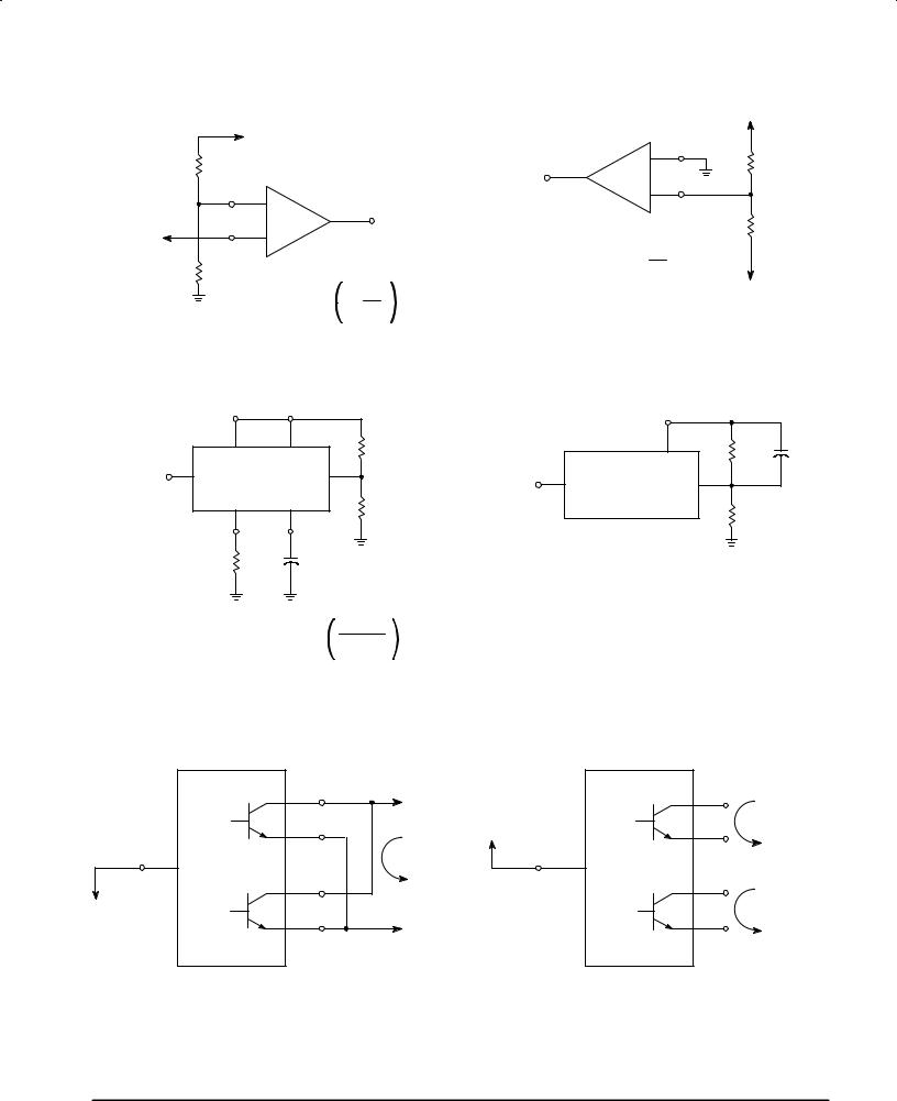
Figure 1. Representative Block Diagram |
|
|
|||||
|
|
|
|
|
|
|
|
|
Output Control |
|
VCC |
|
|
|
|
|
|
|
|
|
13 |
|
|
|
6 |
|
|
|
|
|
|
|
|
|
8 |
|
|
|
|
|
|
|
|
|
|
|
|
|
|
|
Oscillator |
|
|
|
D |
Q |
|
Q1 |
9 |
RT |
5 |
|
|
|
|
|
Flip± |
|
|
|
|
|
|
|
|
|
|
|
|
|
|||
|
CT |
|
|
Deadtime |
|
|
Flop |
|
|
|
|
|
|
|
|
Comparator |
|
|
Ck |
Q |
|
Q2 |
11 |
|
|
|
≈ 0.12V |
± |
|
|
|
||||
|
|
|
+ |
|
|
|
|
|
|
|
|
|
4 |
|
|
|
|
|
|
|
|
10 |
|
|
|
|
|
|
|
|
|
|
|
||
|
|
≈ 0.7V |
|
|
|
|
|
|
|
|
|
|
Deadtime |
|
|
|
|
|
|
|
|
|
|
|
Control |
|
|
± |
|
|
|
|
|
|
12 |
|
|
|
|
|
|
|
|
± |
|
|
|
|
|
|
|
+ |
|
|
|
|
|
VCC |
|
|
|
|
|
|
|
|
+ |
4.9V |
|
||
|
|
|
0.7mA |
PWM |
|
|
UV |
|
|||
|
|
|
Comparator |
|
|
|
|
|
|||
|
|
|
|
|
|
|
Lockout |
± |
|
Reference |
|
|
|
+ |
|
+ |
|
|
|
|
Regulator |
|
|
|
|
|
|
|
|
+ |
|
|
|||
|
|
|
|
|
|
|
|
|
|||
|
|
1 |
|
2 |
|
|
|
|
|
|
|
|
|
|
|
|
|
|
|
|
|
||
|
|
± |
|
± |
|
|
|
3.5V |
|
|
|
|
1 |
2 |
|
3 |
15 |
16 |
|
|
14 |
7 |
|
|
Error Amp |
Feedback PWM |
Error Amp |
|
|
Ref. |
Gnd |
|
|||
|
|
|
|
|
|||||||
|
|
1 |
Comparator Input |
|
2 |
|
|
Output |
|
|
|
This device contains 46 active transistors.
Figure 2. Timing Diagram
Capacitor CT |
Feedback/PWM Comp. |
Deadtime Control |
Flip±Flop |
Clock Input |
Flip±Flop |
Q |
Flip±Flop |
Q |
Output Q1 |
Emitter |
Output Q2 |
Emitter |
Output |
Control |
4 |
MOTOROLA ANALOG IC DEVICE DATA |
TL594
APPLICATIONS INFORMATION
Description
The TL594 is a fixed±frequency pulse width modulation control circuit, incorporating the primary building blocks required for the control of a switching power supply. (See Figure 1.) An internal±linear sawtooth oscillator is frequency± programmable by two external components, RT and CT. The approximate oscillator frequency is determined by:
fosc ≈ |
1.1 |
|
RT •CT |
||
|
For more information refer to Figure 3.
Output pulse width modulation is accomplished by comparison of the positive sawtooth waveform across capacitor CT to either of two control signals. The NOR gates, which drive output transistors Q1 and Q2, are enabled only when the flip±flop clock±input line is in its low state. This happens only during that portion of time when the sawtooth voltage is greater than the control signals. Therefore, an increase in control±signal amplitude causes a corresponding linear decrease of output pulse width. (Refer to the Timing Diagram shown in Figure 2.)
The control signals are external inputs that can be fed into the deadtime control, the error amplifier inputs, or the feedback input. The deadtime control comparator has an effective 120 mV input offset which limits the minimum output deadtime to approximately the first 4% of the sawtooth±cycle time. This would result in a maximum duty cycle on a given output of 96% with the output control grounded, and 48% with it connected to the reference line. Additional deadtime may be imposed on the output by setting the deadtime±control input to a fixed voltage, ranging between 0 V to 3.3 V.
The pulse width modulator comparator provides a means for the error amplifiers to adjust the output pulse width from the maximum percent on±time, established by the deadtime control input, down to zero, as the voltage at the feedback pin varies from 0.5 V to 3.5 V. Both error amplifiers have a
Functional Table
Input/Output |
Output Function |
|
fout |
|
|
Controls |
fosc = |
||||
|
|||||
Grounded |
Single±ended PWM @ Q1 and Q2 |
1.0 |
|||
|
|
|
|||
@ Vref |
Push±pull Operation |
0.5 |
|||
common±mode input range from ±0.3 V to (VCC ± 2 V), and may be used to sense power±supply output voltage and current. The error±amplifier outputs are active high and are ORed together at the noninverting input of the pulse±width modulator comparator. With this configuration, the amplifier that demands minimum output on time, dominates control of the loop.
When capacitor CT is discharged, a positive pulse is generated on the output of the deadtime comparator, which clocks the pulse±steering flip±flop and inhibits the output transistors, Q1 and Q2. With the output±control connected to the reference line, the pulse±steering flip±flop directs the modulated pulses to each of the two output transistors alternately for push±pull operation. The output frequency is equal to half that of the oscillator. Output drive can also be taken from Q1 or Q2, when single±ended operation with a maximum on±time of less than 50% is required. This is desirable when the output transformer has a ringback winding with a catch diode used for snubbing. When higher output±drive currents are required for single±ended operation, Q1 and Q2 may be connected in parallel, and the output±mode pin must be tied to ground to disable the flip±flop. The output frequency will now be equal to that of the oscillator.
The TL594 has an internal 5.0 V reference capable of sourcing up to 10 mA of load current for external bias circuits. The reference has an internal accuracy of ±1.5% with a typical thermal drift of less than 50 mV over an operating temperature range of 0° to 70°C.
f OSC, OSCILLATOR FREQUENCY (Hz)
Figure 3. Oscillator Frequency versus |
Figure 4. Open Loop Voltage Gain and |
Timing Resistance |
Phase versus Frequency |
|
|
|
|
|
|
|
|
|
(dB) |
120 |
|
|
|
|
|
|
|
|
|
|
|
|
|
|
|
VCC = 15 V |
110 |
|
|
|
|
|
|
|
EXCESS PHASE (DEGREES) |
||
|
|
|
|
|
|
|
OPEN LOOP VOLTAGE GAIN |
|
|
|
V |
CC |
= 15 V |
|
||||
|
|
|
|
CT = 0.001 μF |
|
100 |
|
|
|
|
||||||||
|
|
|
|
|
|
|
|
|
|
|
VO = 3.0 V |
0 |
||||||
|
|
|
|
|
|
|
|
|
90 |
|
|
|
RL = 2.0 kΩ |
|||||
|
|
|
|
|
|
|
|
|
80 |
|
|
|
20 |
|||||
|
|
|
|
|
|
|
|
|
|
|
AVOL |
|
|
|
||||
|
|
|
|
|
|
|
|
|
70 |
|
|
|
|
|
40 |
|||
|
|
|
|
|
|
|
|
|
|
|
|
|
|
|
||||
10 k |
|
|
|
0.01 μF |
|
|
|
|
60 |
|
|
|
|
|
|
60 |
||
|
|
|
|
|
|
|
|
50 |
|
|
|
|
|
φ |
80 |
|||
|
|
|
|
|
|
|
|
|
|
|
|
|
|
|||||
|
|
|
|
|
|
|
|
|
40 |
|
|
|
|
|
100 |
|||
|
|
|
|
|
|
|
|
|
|
|
|
|
|
|
||||
|
|
|
|
0.1 μF |
|
|
|
|
30 |
|
|
|
|
|
|
120 |
||
|
|
|
|
|
|
|
|
, |
20 |
|
|
|
|
|
|
140 |
φ , |
|
1.0 k |
|
|
|
|
|
|
|
VOL |
|
|
|
|
|
|
||||
|
|
|
|
|
|
|
|
10 |
|
|
|
|
|
|
160 |
|||
|
|
|
|
|
|
|
|
|
A |
|
|
|
|
|
|
|
||
500 |
2.0 k |
5.0 k |
10 k |
20 k |
50 k |
100 k |
200 k |
500 k |
1.0 M |
0 |
|
|
|
|
|
|
180 |
|
1.0 k |
1.0 |
10 |
100 |
1.0 k |
10 k |
100 k |
1.0 M |
|
||||||||||
|
|
|
RT, TIMING RESISTANCE (Ω) |
|
|
|
|
f, FREQUENCY (Hz) |
|
|
|
|
||||||
MOTOROLA ANALOG IC DEVICE DATA |
5 |
|
TL594
Figure 5. Percent Deadtime versus
Oscillator Frequency
OUTPUT) |
20 |
|
|
|
|
18 |
|
|
|
|
|
16 |
|
|
|
|
|
(EACH |
|
CT = 0.001 |
μF |
||
14 |
|
||||
|
|
|
|
||
DEADTIME |
12 |
|
|
|
|
10 |
|
|
|
|
|
8.0 |
|
|
|
|
|
PERCENT |
|
|
|
|
|
6.0 |
|
0.01 |
μF |
|
|
4.0 |
|
|
|||
|
|
|
|
||
|
|
|
|
|
|
% DT, |
2.0 |
|
|
|
|
0 |
|
|
|
|
|
|
|
|
|
|
|
|
500 k |
1.0 k |
10 k |
100 k |
500 k |
|
|
|
fosc, OSCILLATOR FREQUENCY (Hz) |
|
|
Figure 6. Percent Duty Cycle versus
Deadtime Control Voltage
OUTPUT) |
50 |
|
|
|
|
|
|
1 |
|
|
|
||
(EACH |
40 |
VCC = 15 V |
|
|||
|
|
|||||
|
2 |
VOC = Vref |
|
|||
|
|
1. |
CT = 0.01 μF |
|
||
CYCLE |
|
|
|
|||
30 |
|
1. |
RT = 10 kΩ |
|
||
|
|
2. |
CT = 0.001 μF |
|
||
DUTY |
20 |
|
1. |
RT = 30 kΩ |
|
|
|
|
|
|
|||
|
|
|
|
|
||
DC, PERCENT |
10 |
|
|
|
|
|
0 |
|
|
|
|
||
% |
|
|
|
|
||
0 |
1.0 |
2.0 |
3.0 |
3.5 |
||
|
||||||
VDT, DEADTIME CONTROL VOLTAGE (IV)
Figure 7. Emitter±Follower Configuration
Output Saturation Voltage versus
Emitter Current
|
1.9 |
|
|
|
|
(V) |
1.8 |
|
|
|
|
VOLTAGE |
|
|
|
|
|
1.7 |
|
|
|
|
|
1.6 |
|
|
|
|
|
, SATURATION |
|
|
|
|
|
1.5 |
|
|
|
|
|
1.4 |
|
|
|
|
|
1.3 |
|
|
|
|
|
CE(sat) |
|
|
|
|
|
1.2 |
|
|
|
|
|
V |
|
|
|
|
|
|
1.1 |
|
|
|
|
|
0 |
100 |
200 |
300 |
400 |
IE, EMITTER CURRENT (mA)
Figure 9. Standby Supply Current
versus Supply Voltage
|
10 |
|
|
|
|
|
|
|
|
(mA) |
9.8 |
|
|
|
|
|
|
|
|
8.0 |
|
|
|
|
|
|
|
|
|
|
|
|
|
|
|
|
|
|
|
CURRENT |
7.0 |
|
|
|
|
|
|
|
|
6.0 |
|
|
|
|
|
|
|
|
|
5.0 |
|
|
|
|
|
|
|
|
|
, SUPPLY |
|
|
|
|
|
|
|
|
|
4.0 |
|
|
|
|
|
|
|
|
|
3.0 |
|
|
|
|
|
|
|
|
|
CC |
2.0 |
|
|
|
|
|
|
|
|
I |
|
|
|
|
|
|
|
|
|
|
1.0 |
|
|
|
|
|
|
|
|
|
0 |
|
|
|
|
|
|
|
|
|
0 |
5.0 |
10 |
15 |
20 |
25 |
30 |
35 |
40 |
VCC, SUPPLY VOLTAGE (V)
Figure 8. Common±Emitter Configuration
Output Saturation Voltage versus
Collector Current
|
2.0 |
|
|
|
|
(V) |
1.8 |
|
|
|
|
VOLTAGE |
1.6 |
|
|
|
|
1.4 |
|
|
|
|
|
, SATURATION |
1.2 |
|
|
|
|
1.0 |
|
|
|
|
|
0.8 |
|
|
|
|
|
CE(sat) |
|
|
|
|
|
0.6 |
|
|
|
|
|
|
|
|
|
|
|
V |
0.4 |
|
|
|
|
|
|
|
|
|
|
|
0 |
100 |
200 |
300 |
400 |
IC, COLLECTOR CURRENT (mA)
Figure 10. Undervoltage Lockout Thresholds
(V) |
|
|
versus Reference Load Current |
|
|
|||||
|
|
|
|
|
|
|
|
|
||
THRESHOLD |
6.0 |
|
|
|
|
|
|
|
|
|
5.5 |
|
|
|
Turn On |
|
|
|
|
||
|
|
|
|
|
|
|
|
|||
LOCKOUT |
5.0 |
|
|
|
Turn Off |
|
|
|
|
|
|
|
|
|
|
|
|
|
|||
, UNDERVOLTAGE |
4.5 |
|
|
|
|
|
|
|
|
|
4.0 |
|
|
|
|
|
|
|
|
||
TH |
|
|
|
|
|
|
|
|
||
0 |
5.0 |
10 |
15 |
20 |
25 |
30 |
35 |
40 |
||
V |
||||||||||
|
|
|
IL, REFERENCE LOAD CURERNT (mA) |
|
|
|||||
6 |
MOTOROLA ANALOG IC DEVICE DATA |
TL594
Figure 11. Error±Amplifier Characteristics |
Figure 12. Deadtime and Feedback Control Circuit |
|
|
Error Amplifier |
|
VCC = 15V |
150 |
150 |
|
|
+ |
Under Test |
|
|
VCC |
2W |
2W |
Vin |
|
|
|
|
|
|
|
± |
|
Test |
Deadtime |
C1 |
Output 1 |
||
|
|
||||||
|
|
|
|
|
E1 |
|
|
|
|
Feedback |
Inputs |
Feedback |
|
||
|
|
|
|
||||
|
|
|
|
|
|||
|
|
Terminal |
|
RT |
|
C2 |
Output 2 |
|
|
(Pin 3) |
|
CT |
|
E2 |
|
|
|
|
|
|
|
|
|
|
+ |
|
|
(+) |
|
|
|
Vref |
± |
|
|
(±) |
Error |
|
|
|
|
(+) |
|
|
|||
Other Error |
|
|
|
|
|||
|
|
|
(±) |
|
|
|
|
|
|
Amplifier |
|
|
Ref |
|
|
|
|
|
Output |
|
|
||
|
|
|
|
|
|
||
|
|
|
|
|
Out |
|
|
|
|
|
50k |
Control |
|
|
|
|
|
|
Gnd |
|
|
||
|
|
|
|
|
|
||
Figure 13. Common±Emitter Configuration |
Figure 14. Emitter±Follower Configuration |
||||
Test Circuit and Waveform |
Test Circuit and Waveform |
||||
|
|
15V |
|
|
|
|
|
RL |
|
15V |
|
|
|
|
C |
|
|
|
|
68 |
|
|
|
|
|
VC |
Each |
|
|
|
|
C |
Output |
Q |
|
Each |
|
CL |
Transistor |
|
VEE |
Output |
Q |
|
E |
||
Transistor |
|
15pF |
|
|
|
|
|
|
RL |
CL |
|
|
|
E |
|
||
|
|
|
68 |
15pF |
|
90% |
|
90% |
90% |
|
90% |
|
|
|
VEE |
||
VCC |
|
|
|
|
|
|
|
10% |
|
10% |
|
10% |
|
10% |
|
||
|
Gnd |
|
|
||
|
tr |
tf |
tr |
|
tf |
|
|
|
|
||
MOTOROLA ANALOG IC DEVICE DATA |
7 |
|
|
|
|
|
TL594 |
|
|
|
|
Figure 15. Error±Amplifier Sensing Techniques |
|
|
||||
VO |
To Output |
|
|
|
|
|
Vref |
|
|
|
|
|
|
||
|
Voltage of |
|
|
|
|
|
1 |
|
System |
|
|
|
|
+ |
|
R1 |
|
|
|
|
|
R2 |
|
|
|
|
3 |
Error |
|
||
|
|
|
|
|
|
||
|
|
|
|
Amp |
|
|
|
1 |
|
|
|
|
± |
|
|
+ |
|
|
|
|
2 |
||
|
|
|
|
|
|
||
|
Error |
|
|
|
|
|
|
|
|
3 |
|
|
|
|
|
|
Amp |
|
|
Negative Output Voltage |
R1 |
||
Vref |
|
|
|
||||
± |
|
|
|
|
|
|
|
2 |
|
|
|
|
VO = Vref |
R1 |
|
R2 |
Positive Output Voltage |
|
R2 |
VO |
|||
|
|
||||||
|
|
|
|
|
|
|
|
|
VO = Vref |
1 + |
R1 |
|
|
|
To Output |
|
R2 |
|
|
|
Voltage of |
||
|
|
|
|
|
|
System |
|
|
|
|
|
|
|
|
|
Figure 16. Deadtime Control Circuit |
|
Figure 17. Soft±Start Circuit |
|||||
Output |
|
|
|
|
|
|
|
Control |
|
|
|
|
|
|
|
Output |
Vref |
4 |
R1 |
|
|
Vref |
CS |
|
|
Output |
|
4 |
|||
Q |
DT |
|
|
Q |
|
||
|
|
|
|
||||
RT |
CT |
|
|
|
|
DT |
|
|
R2 |
|
|
|
RS |
||
6 |
5 |
|
|
|
|
||
|
|
|
|
|
|||
30k |
0.001 |
|
|
|
|
|
|
80
Max. % on Time, each output ≈ 45 ±
1 + R1R2
Figure 18. Output Connections for Single±Ended and Push±Pull Configurations
|
|
C1 |
|
C1 |
|
|
Q1 |
QC |
2.4 V ≤ VOC ≤ Vref |
1 |
1.0 mA to 250 mA |
|
1 |
Q1 |
|||
|
|
E |
|
E |
|
Output |
|
1.0 mA to |
Output |
|
|
Control |
|
Control |
|
|
|
|
500 mA |
|
|
||
|
Single±Ended |
Push±Pull |
|
|
|
|
C2 |
C2 |
|
||
|
|
|
|
||
0 ≤ VOC ≤ 0.4 V |
Q2 |
E2 |
Q2 |
E2 |
1.0 mA to 250 mA |
|
|||||
|
|
QE |
|
|
|
8 |
MOTOROLA ANALOG IC DEVICE DATA |
|
TL594 |
Figure 19. Slaving Two or More Control Circuits |
Figure 20. Operation with Vin > 40 V Using |
Vref |
External Zener |
|
|
R |
|
VCC |
|
S |
|
|
6 |
Vin > 40V |
1N975A |
12 |
|
RT |
|
|
5 |
Master |
VZ = 39V |
5.0V |
RT |
CT |
|
Ref |
CT |
|
270 |
|
|
|
Gnd |
|
|
|
|
Vref |
7 |
6 |
|
RT |
Slave |
5 |
(Additional |
CT |
Circuits) |
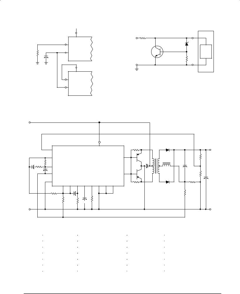
Figure 21. Pulse Width Modulated Push±Pull Converter
+Vin = 8.0V to 20V |
|
|
|
|
|
|
|
|
|
|
|
|
|
|
|
|
|
|
||
|
|
|
|
|
|
|
|
|
|
|
12 |
|
|
47 |
|
|
|
|
+VO = 28V |
|
|
|
1 |
|
|
|
|
|
|
|
|
VCC |
|
|
|
1N4934 |
|
|
IO = 0.2A |
||
|
|
+ |
|
|
|
|
|
|
|
|
|
|
|
T1 |
|
|
|
|
||
|
|
2 |
± |
|
|
|
|
|
|
|
|
|
8 |
Tip |
|
|
|
22 |
|
|
|
1.0M |
|
|
|
|
|
|
|
|
|
|
C1 |
32 |
|
L1 |
|
k |
|
|
|
|
|
|
|
|
|
|
|
|
|
|
|
|
|
+ |
|
|
|
|||
|
33k |
3 |
Comp |
|
|
|
|
TL594 |
|
|
|
|
|
|
|
50 |
|
|
||
|
|
|
|
|
|
|
|
|
|
|
+ |
|
|
|
|
|||||
0.01 |
0.01 |
15 |
|
|
|
|
|
|
|
|
|
|
11 |
|
|
|
35V |
|
|
|
± |
|
|
|
|
|
|
|
|
|
Tip |
50 |
|
|
|
|
|
||||
|
|
|
|
|
|
|
|
|
|
|
|
|
|
|
|
|||||
|
|
|
|
|
|
|
|
|
|
|
|
|
C2 |
32 |
25V |
|
|
4.7k |
+ |
50 |
|
|
16 |
+ |
OC |
V |
REF |
DT |
C |
R |
|
Gnd |
E1 |
E2 |
47 |
|
|
|
1.0 |
|
35V |
|
|
|
|
|
|
|
T |
T |
|
|
|
|
1N4934 |
|
|
|
||||
|
|
|
13 |
14 |
|
4 |
5 |
6 |
|
7 |
9 |
10 |
|
|
|
|
|
|
||
|
|
|
+ |
|
|
|
|
|
|
|
|
|||||||||
|
|
|
|
|
|
|
|
|
|
|
|
|
|
|
|
240 |
|
|
|
|
|
|
|
|
|
|
|
|
|
|
|
|
|
|
|
|
|
|
|
|
|
|
|
|
4.7k |
|
|
10 |
|
|
15k |
|
|
|
|
|
|
|
|
|
||
|
|
|
4.7k |
|
|
|
|
|
|
|
|
|
|
|
|
|
||||
|
|
|
|
|
10k |
0.001 |
|
|
|
|
|
|
|
|
|
|
||||
|
|
|
|
|
|
|
|
|
|
|
|
|
|
|
|
|
||||
|
|
|
|
|
|
|
|
|
|
|
|
|
|
|
|
|
|
|||
All capacitors in μF
Test |
|
Conditions |
Results |
|
|
|
|
|
|
L1 ± 3.5 mH @ 0.3 A |
|
Line Regulation |
Vin = 10 V to 40 V |
14 mV 0.28% |
|||
T1 ± Primary: 20T C.T. #28 AWG |
|||||
Load Regulation |
Vin = 28 |
V, IO = 1.0 mA to 1.0 A |
3.0 mV 0.06% |
Secondary: 12OT C.T. #36 AWG |
|
|
|
|
|
Core: Ferroxcube 1408P±L00±3CB |
|
Output Ripple |
Vin = 28 |
V, IO = 1.0 A |
65 mVpp P.A.R.D. |
||
|
|||||
Short Circuit Current |
Vin = 28 |
V, RL = 0.1 Ω |
1.6 A |
|
|
Efficiency |
Vin = 28 |
V, IO = 1.0 A |
71% |
|
|
MOTOROLA ANALOG IC DEVICE DATA |
9 |
|
|
|
|
|
|
|
|
|
TL594 |
|
|
|
|
|
|
|
|
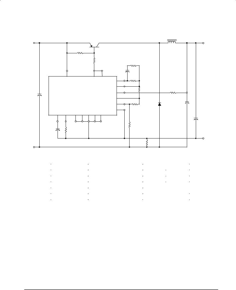
Figure 22. Pulse Width Modulated Step±Down Converter |
|
|
||||||||
+Vin = 10V to 40V |
|
|
|
|
|
|
|
|
|
1.0mH @ 2.0A |
|
||
|
|
|
Tip 32A |
|
|
|
|
|
|
+VO = 5.0V |
|||
|
|
|
|
|
|
|
|
|
|
|
|
|
IO = 1.0A |
|
|
|
|
47 |
|
|
|
|
|
|
|
|
|
|
|
|
|
|
|
150 |
|
|
47k |
|
|
|
|
|
|
|
|
|
|
|
|
|
|
|
|
|
|
|
|
12 |
|
|
8 |
11 |
|
0.1 |
|
|
|
|
|
|
|
|
|
|
|
|
|
|
|
|
|||
|
|
VCC |
|
|
|
C1 |
C2 |
Comp |
3 |
1.0M |
|
|
|
|
|
|
|
|
|
|
|
|
|||||
|
|
|
|
|
|
|
|
|
|
|
|
|
|
|
|
|
|
|
|
|
|
± |
2 |
|
|
|
|
|
|
|
|
|
|
|
|
|
|
|
|
|
|
|
+ |
|
|
|
|
|
|
+ |
1 |
5.1k |
5.1k |
|
|
50 |
|
|
|
|
|
|
|
|
|
|
|||
|
|
|
|
|
|
|
|
|
|
|
|||
|
|
TL594 |
|
|
|
|
14 |
|
|
|
|
||
50V |
|
|
|
|
|
Vref |
|
|
|
+ |
|||
|
|
|
|
|
|
|
|
15 |
|
|
500 |
||
|
|
|
|
|
|
|
|
± |
|
MR850 |
|
||
|
|
|
|
|
|
|
|
5.1k |
10V |
|
|||
|
|
|
|
|
|
|
|
+ |
16 |
|
|
|
|
|
CT |
RT |
D.T. |
O.C. Gnd |
E1 |
E2 |
|
|
|
|
|||
|
|
|
|
|
|
+ |
|||||||
|
5 |
6 |
4 |
13 |
7 |
9 |
10 |
|
|
|
|
|
|
|
|
|
|
|
|
50 |
|||||||
|
|
|
|
|
|
|
|
|
|
150 |
|
|
10V |
|
|
|
|
|
|
|
|
|
|
|
|
|
|
|
0.001 |
47k |
|
|
|
|
|
|
|
|
|
|
|
|
|
|
|
|
|
|
|
|
|
|
0.1 |
|
|
Test |
Conditions |
Results |
|
|
|
|
|
Line Regulation |
Vin = 8.0 V to 40 V |
3.0 mV |
0.01% |
Load Regulation |
Vin = 12.6 V, IO = 0.2 mA to 200 mA |
5.0 mV |
0.02% |
Output Ripple |
Vin = 12.6 V, IO = 200 mA |
40 mVpp |
P.A.R.D. |
Short Circuit Current |
Vin = 12.6 V, RL = 0.1 Ω |
250 mA |
|
Efficiency |
Vin = 12.6 V, IO = 200 mA |
72% |
|
10 |
MOTOROLA ANALOG IC DEVICE DATA |