

схемы для компов БП / Схемы АТ, АТХ / AT30
.PDFT E C H N O L O G Y |
AT30 |
High Performance Off-line Controller
Description
The AT30 is a high performance green-energy offline power supply controller. It features a scalable driver for driving external NPN or MOSFET transistors for line voltage switching. This proprietary architecture enables many advanced features to be integrated into a small package (TO-92 or SOT23-5), resulting in lowest total cost solution.
The AT30 design has 6 internal terminals and is a pulse frequency and width modulation IC with many flexible packaging options. One combination of internal terminals is packaged in the space-saving TO-92 package (A/B/C/D versions) for 65kHz or 100kHz switching frequency and with 400mA or 800mA current limit. The E version (SOT23-5) can be configured for higher current limit.
Consuming only 0.15W in standby, the IC features over-current, hiccup mode short circuit, and under-voltage protection mechanisms. The AT30 is ideal for use in high performance universal adaptors and chargers.
Applications
Offline PWM AC/DC converter for
●Battery Charger
●Power Adaptor
●Universal Off-line Power Supplies
●Standby Power Supplies
Features
●High Performance with 0.15W Standby Power
●Current Mode Operation
●PWM/Pulse-Skipping Switching Control
●Emitter Drive Allows Safe NPN Flyback Use
●65kHz or 100kHz Switching Frequency
●Leading Edge Blanking
●Complete Protection Circuits including
Over-Current Protection, Under-Voltage Protection and Hiccup Mode for Short Circuit
●Flexible Packaging Options(including TO-92)
●Selectable 0.4A to 1.2A Current Limit
●Lowest Total Cost Solution
HIGH VOLTAGE DC
R1
D2 |
Q1 |
|
|
R2 |
|
IC1
DRV
AT30 VDD  OPTOCOUPLER
 C1
C1 

 D1
D1
GND
Figure1. Simplified Application Circuit of AT30
http://www.sirectsemi.com/atc |
1 |

T E C H N O L O G Y |
AT30 |
Ordering Information
|
Part Number |
|
|
Switching Frequency |
|
|
Current Limit |
|
|
Temperature Range |
|
|
Package |
|
|
Pins |
|
|
|
|
|
|
|
|
|
|
|
|
|
||||||
|
AT30A |
|
|
65kHz |
|
|
400mA |
|
|
-40°C to 85°C |
|
|
To-92 |
|
3 |
|
|
|
AT30B |
|
|
65kHz |
|
|
800mA |
|
|
-40°C to 85°C |
|
|
To-92 |
|
3 |
|
|
|
AT30C |
|
|
100kHz |
|
|
400mA |
|
|
-40°C to 85°C |
|
|
To-92 |
|
3 |
|
|
|
AT30D |
|
|
100kHz |
|
|
800mA |
|
|
-40°C to 85°C |
|
|
To-92 |
|
3 |
|
|
|
AT30E |
|
|
Selectable |
|
|
Adjustable |
|
|
-40°C to 85°C |
|
|
SOT23-5 |
|
5 |
|
|
Pin Assignments
TO-92
SOT23-5
AT30A
AT30B
AT30C |
AT30E |
|
AT30D
Functional Pin Description |
|
||
Pin Number |
PIN |
|
|
|
|
|
|
TO-92 |
SOT23-5 |
NAME |
Pin Function |
|
|
||
1 |
1 |
VDD |
Power Supply Pin. Connect to optocoupler's emitter. Internally limited to 5.5V max. |
|
Bypass to GND with a proper compensation network. |
||||
|
|
|
||
|
|
|
|
|
2 |
2 |
GND |
Ground |
|
|
|
|
|
|
|
|
|
Driver Output (TO-92 Only). Connect to emitter of the high voltage NPN or MOSFET. For |
|
3 |
|
DRV |
AT30A/C, DRV pin is internally connected to DRV1. For AT30B/D, DRV pin is internally |
|
|
|
|
connected to both DRV1 and DRV2. |
|
|
|
|
|
|
|
5 |
DRV1 |
Driver Output 1 (SOT23-5 Only). Also used as supply input during startup. |
|
|
|
|
|
|
|
4 |
DRV2 |
Driver Output 2 (SOT23-5 Only) |
|
|
|
|
|
|
|
|
|
Frequency Select (SOT23-5 Only). This terminal has an internal 200kΩ pull down |
|
|
3 |
FREQ |
resistor. Connect to VDD for 100kHz operation. Connect to GND or leave unconnected for |
|
|
|
|
65kHz operation. |
http://www.sirectsemi.com/atc |
2 |

T E C H N O L O G Y |
|
|
AT30 |
|
Absolute Maximum Ratings |
Thermal Information |
|
||
● VDD,FREQ Voltage |
0.3V to + 6V |
● Junction Temperature------------------------- - |
40°C to +150°C |
|
|
|
|||
● VDD current--------------------------------------------------- |
20mA ● Storage Temperature Range---------------- - |
55°C to +150°C |
||
● VDRV, DRV1, DRV2 Voltage ---------------- |
-0.3V to + 18V |
● Lead Temperature (Soldering, 10sec) ------------------ |
300°C |
|
● Continuous DRV, |
|
ESD Classification |
|
|
DRV1, DRV2 Current |
Internally limited |
|
||
|
|
|||
●Maximum Power Dissipation |
0.6W for TO-92 |
● Human Body Model----------------------------------- |
2000V |
|
● Machine Model |
200V |
|||
0.39W for SOT23-5 |
||||
|
||||
|
|
|
||
Note Stresses beyond those listed under “Absolute Maximum Ratings" may cause permanent damage to the device.
Electrical Characteristics
(TA = 25°C, VDD=4V if not otherwise noted)
|
Parameter |
|
|
Symbol |
|
|
Test Conditions |
|
|
Min |
|
|
Typ |
|
|
Max |
|
|
Units |
|
||
|
|
|
|
|
|
|
|
|
|
|
|
|
|
|||||||||
|
VDD Start Voltage |
|
|
VSTART |
|
Rising edge |
|
|
4.75 |
|
5 |
|
5.25 |
|
V |
|||||||
|
|
|
|
|
|
|
|
|
|
|
|
|
|
|
|
|
||||||
|
VDD Clamp Voltage |
|
|
VDD_CLP |
|
I(VDD)=10mA |
|
|
5.15 |
|
5.45 |
|
5.75 |
|
V |
|||||||
|
|
|
|
|
|
|
|
|
|
|
|
|
|
|
|
|
|
|
||||
|
Supply Current |
|
|
IDD |
|
|
|
|
|
|
|
|
0.7 |
|
0.1 |
|
|
mA |
||||
|
|
|
|
|
|
|
|
|
|
|
|
|
|
|
|
|||||||
|
Startup Supply Current |
|
|
IDDST |
|
VDD = 4V before VUV |
|
|
|
0.23 |
|
0.45 |
|
mA |
||||||||
|
|
|
|
|
|
|
|
|
|
|
|
|
|
|
|
|
||||||
|
VDD Under-Voltage Threshold |
|
|
UUV |
|
Falling edge |
|
|
3.17 |
|
3.35 |
|
3.53 |
|
V |
|||||||
|
|
|
|
|
|
|
|
|
|
|
|
|
|
|
|
|
|
|
|
|
|
|
|
|
|
|
|
|
|
DRV1 must be |
|
AT30A/C |
|
|
|
8.6 |
|
10.5 |
|
|
|
||||
|
|
|
|
|
|
|
|
|
|
|
|
|
|
|
|
|||||||
|
DRV1 Start Voltage |
|
|
VDRVST |
|
higher than this |
|
|
|
|
|
|
|
|
|
|
|
|
|
V |
||
|
|
|
|
|
AT30B/D |
|
|
|
9.6 |
|
11.5 |
|
|
|||||||||
|
|
|
|
|
|
|
voltage to start up. |
|
|
|
|
|
|
|
|
|
||||||
|
|
|
|
|
|
|
|
|
|
|
|
|
|
|
|
|
|
|
|
|
|
|
|
DRV1 Short-Circuit Detect Threshold |
|
|
VDRVSC |
|
AT30A/C |
|
|
|
|
|
6.8 |
|
|
|
|
|
V |
||||
|
|
|
|
|
|
|
|
|
|
|
|
|
|
|
|
|
|
|||||
|
|
|
|
|
|
|
AT30A/B or FREQ = 0 |
55 |
|
65 |
|
85 |
|
|
|
|
||||||
|
Switching frequency |
|
|
FSW |
|
|
|
|
|
|
|
|
|
|
|
|
|
|
|
kHz |
||
|
|
|
|
AT30C/D or FREQ = VDD |
75 |
|
100 |
|
125 |
|
|
|||||||||||
|
|
|
|
|
|
|
|
|
|
|
|
|
||||||||||
|
|
|
|
|
|
|
|
|
|
|
|
|
|
|
|
|
|
|||||
|
Maximum Duty Cycle |
|
|
DMAX |
|
VDD=4V |
|
|
67 |
|
75 |
|
83 |
|
% |
|
||||||
|
|
|
|
|
|
|
|
|
|
|
|
|
|
|
|
|
|
|
|
|
||
|
Minimum Duty Cycle |
|
|
DMIN |
|
VDD=4.6V |
|
|
|
|
|
3.5 |
|
|
|
|
% |
|
||||
|
|
|
|
|
|
|
|
|
|
|
|
|
|
|
|
|
|
|
|
|
||
|
|
|
|
|
|
|
|
|
AT30A/C |
|
|
|
400 |
|
|
|
|
|
|
|
||
|
Effective Current Limit |
|
|
ILIM |
|
VDD=VUV+0.1V |
|
|
|
|
|
|
|
|
|
|
|
|
|
mA |
||
|
|
|
|
|
AT30B/D |
|
|
|
800 |
|
|
|
|
|
||||||||
|
|
|
|
|
|
|
|
|
|
|
|
|
|
|
|
|
|
|
||||
|
|
|
|
|
|
|
|
|
|
|
|
|
|
|
|
|
|
|
||||
|
VDD to DRV1 Current Coefficient |
|
|
GGAIN |
|
|
|
|
|
|
|
|
-0.29 |
|
|
|
|
A/V |
||||
|
|
|
|
|
|
|
|
|
|
|
|
|
|
|
|
|
|
|
|
|||
|
VDD Dynamic Impedance |
|
|
RVDD |
|
|
|
|
|
|
|
|
9 |
|
|
|
|
|
kΩ |
|||
|
|
|
|
|
|
|
|
|
|
|
|
|
|
|
|
|
||||||
|
DRV1/DRV2 Driver On-Resistance |
|
|
RDRV1, 2 |
|
IDRV1 = IDRV2 = 0.05A |
|
|
|
3.6 |
|
|
|
|
|
Ω |
||||||
|
|
|
|
|
|
|
|
|
|
|
|
|
|
|
|
|
|
|||||
|
DRV1 Rise Time |
|
|
|
|
|
1nF load, 15Ω pull-up |
|
|
|
30 |
|
|
|
|
|
ns |
|||||
|
|
|
|
|
|
|
|
|
|
|
|
|
|
|
|
|
|
|||||
|
DRV1 Fall Time |
|
|
|
|
|
1nF load, 15Ω pull-up |
|
|
|
20 |
|
|
|
|
|
ns |
|||||
|
|
|
|
|
|
|
|
|
|
|
|
|
|
|
|
|
||||||
|
DRV1 and DRV2 Switch Off Current |
|
|
|
|
|
Driver off, VDRV1 = VDRV2 = 10V |
|
|
|
12 |
|
30 |
|
|
μA |
||||||
|
|
|
|
|
|
|
|
|
|
|
|
|
|
|
|
|
|
|
|
|
|
|
http://www.sirectsemi.com/atc |
3 |
T E C H N O L O G Y
Operation Description
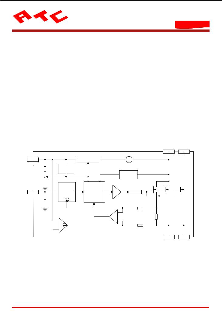
Figure 2 shows the Functional Block Diagram of the AT30. The main components include switching control logic, two on-chip medium-voltage power-MOSFETs with parallel current sensor, driver, oscillator and ramp generator, current limit VC generator, error comparator, hiccup control, bias and undervoltage-lockout, and regulator circuitry.
As seen in Figure 2, the design has 6 internal terminals. VDD is the power supply terminal. DRV1 and DRV2 are linear driver outputs that can drive the emitter of an external high voltage NPN transistor or
AT30
N-channel MOSFET. This emitter-drive method takes advantage of the high VCBO of the transistor, allowing a low cost transistor such as ‘13003 (VCBO
= 700V) or ‘13002 (VCBO = 600V) to be used for a wide AC input range. The slew-rate limited driver coupled with the turn-off characteristics of an external NPN result in lower EMI.
The driver peak current is designed to have a negative voltage coefficient with respect to supply voltage VDD, so that lower supply voltage automatically results in higher DRV1 peak current. This way, the optocoupler can control VDD directly to affect driver current.
|
|
|
|
|
|
DRV1 |
DRV2 |
VDD |
|
REGULATOR |
- |
+ |
|
|
|
|
BIAS & |
|
3.6V(AT30A/C) |
|
|
|
|
9k |
|
4.6V(AT30B/D) |
|
|
|
||
UVLO |
|
|
|
|
|||
|
|
|
|
|
|
||
|
|
HICCUP |
|
|
|
||
|
|
|
|
|
|
||
|
|
|
CONTROL |
|
|
|
|
|
|
PWM/PULSE |
|
|
|
|
|
|
OSC & |
-SKIPPING |
|
|
|
|
|
FREQ |
RAMP |
SWITCHING |
|
SLEW |
1x |
56x |
56x |
|
CURRENT |
CONTROL |
|
|
|||
200k |
|
|
|
|
|
||
|
|
|
|
|
|
|
|
|
|
LOGIC |
|
|
|
|
|
|
|
|
|
20k |
|
|
|
|
|
ERROR |
+ |
|
|
|
|
|
|
COMP |
|
|
|
|
|
|
ILIM VC |
|
|
|
|
|
|
|
|
|
|
|
40 |
|
|
|
- GENERATOR |
|
|
|
|
||
|
- |
20k |
|
|
|
||
4.75V |
+ |
|
|
|
|
|
|
|
|
|
|
|
|
GND |
GND |
Figure 2. Block Diagram of AT30
http://www.sirectsemi.com/atc |
4 |

T E C H N O L O G Y
Startup Sequence
Figure 1 shows a Simplified Application Circuit for the AT30. Initially, the small current through resistor R1 charges up the capacitor C1, and the BJT acts as a follower to bring up the DRV1 voltage. An internal regulator generates a VDD voltage equal to VDRV1 – 3.6V for AT30A/C (VDRV1 – 4.6V for AT30B/D) but limits it to 5.5V max. As VDD crosses 5V, the regulator sourcing function stops and VDD begins to drop due to its current consumption. As VDD voltage decreases below 4.75V, the IC starts to operate with increasing driver current. When the output voltage reaches regulation point, the optocoupler feedback circuit stops VDD from decreasing further. The switching action also allows the auxiliary windings to take over in supplying the C1 capacitor. Figure 3 shows a typical startup sequence for the AT30.
To limit the auxiliary voltage, use a 12V zener diode for AT30A/C or a 13V zener for AT30B/D (D1 diode in Figure 1).
Even though up to 2MΩ startup resistor (R1) can be used due to the very low startup current, the actual R1 value should be chosen as a compromise between standby power and startup time delay.
AT30
Normal Operation
In normal operation, the feedback signal from the secondary side is transmitted through the optocoupler as a current signal into VDD pin, which has dynamic impedance of 9kΩ. The resulting VDD voltage affects the switching of the IC. As seen from the Functional Block Diagram, the Current Limit VC Generator uses the VDD voltage difference with 4.75V to generate a proportional offset at the negative input of the Error Comparator.
The drivers turn on at the beginning of each switching cycle. The current sense resistor current, which is a fraction of the transformer primary current, increases with time as the primary current increases. When the voltage across this current sense resistor plus the oscillator ramp signal equals Error Comparator's negative input voltage, the drivers turn off. Thus, the peak DRV1 current has a negative voltage coefficient of -0.29A/V and can be calculated from the following:
IDRV1PEAK = 0.29A/V • (4.75V – VDD)
for VDD < 4.75V and duty cycle < 50%.
When the output voltage is lower than regulation,
Figure 3. Startup Waveforms
http://www.sirectsemi.com/atc |
5 |

T E C H N O L O G Y
the current into VDD pin is zero and VDD voltage decreases. At VDD = VUV = 3.3V, the peak DRV1 current has maximum value of 400mA.
Current Limit Adjustment
The IC's proprietary driver arrangement allows the current limit to be easily adjusted between 400mA and 1.2A. To understand this, the drivers have to be utilized as linear resistive devices with typically 3.6 (rather than as digital output switches). The current limit can then be calculated through linear combination as shown in Figure 4. For TO-92 package, the AT30A/C are preprogrammed to 400mA current limit and the AT30B/D are preprogrammed to 800mA current limit. For AT30E (SOT23-5) packages, both DRV1 and DRV2 terminals are provided.
DRV1 
 ILIM
ILIM
DRV2
DRV1
DRV2 
 ILIM
ILIM
RD
DRV1
DRV2  I LIM
I LIM
RD
DRV1
ILIM
DRV2
400mA
|
|
|
|
7.2 RD |
|
400mA |
|
|
|
||
|
3.6 RD |
|
800mA
R
400mA D 2
3.6
Figure 4. Driver Output Configurations
Pulse Skipping
The PWM/Pulse Skipping Switching Control Logic block operates in different modes depending on the output load current level. At light load, the VDD voltage is around 4.75V. The energy delivered by
AT30
each switching cycle (with minimum on time of 500ns) to the output causes VDD to increase slightly above 4.75V. The PWM Switching Control Logic block is able to detect this condition and prevents the IC from switching until VDD is below 4.75V again. This results in a pulse-skipping action with fixed pulse width and varying frequency, and low power consumption because the switching frequency is reduced. Typical system standby power consumption is 0.15W.
Short Circuit Hiccup
When the output is short circuited, the AT30 enters hiccup mode operation. In this condition, the auxiliary supply voltage collapses. An on-chip detector compares DRV1 voltage during the off-time of each cycle to 6.8V. If DRV1 voltage is below 6.8V, the IC will not start the next cycle, causing both the auxiliary supply voltage and VDD to reduce further. The circuit enters startup mode when VDD drops below 3.3V. This hiccup behavior continues until the short circuit is removed. In this behavior, the effective duty cycle is very low resulting in very low short circuit current.
To make sure that the IC enters hiccup mode easily, the transformer should be constructed so that there is close coupling between secondary and auxiliary, so that the auxiliary voltage is low when the output is short-circuited. This can be achieved with the primary/auxiliary/secondary sequencing from the bobbin.
http://www.sirectsemi.com/atc |
6 |

T E C H N O L O G Y
Application Example
The application circuit in Figure 6 provides a 5V/0.75A constant voltage/constant current output. An AT30 is used in combination with the TL431 for highest efficiency and lowest component count. To change the constant output voltage VOUTCV and constant current limit IOUTCC, modify R7 and R6 as following:
R7 = 80kΩ • [(VOUTCV -1V)/3.8V - 1] R6 = 250mV/IOUTCC
The performance of this circuit is summarized in Table 1.
Table 1. System Performance of Circuit in Figure 6
|
110VAC |
220VAC |
|
|
|
Standby Power |
0.09W |
0.15W |
|
|
|
Current Limit |
0.75A |
0.75A |
|
|
|
Full Load Efficiency |
65% |
67% |
|
|
|
RF1
AT30
Layout Considerations
The following should be observed when doing layout for the AT30:
1.Use a "star point" connection at the GND pin of AT30 for the VDD bypass components (C5 and C6 in Figure 6), the input filter capacitor (C2 in Figure 6) and other ground connections on the primary side.
2.Keep the loop across the input filter capacitor, the transformer primary windings, and the high voltage transistor, and the AT30 as small as possible.
3.Keep AT30 pins and the high voltage transistor pins as short as possible.
4.Keep the loop across the secondary windings, the output diode, and the output capacitors as small as possible.
5.Allow enough copper area under the high voltage transistor, output diode, and current shunt resistor for heat sink.
AC1 |
|
|
|
|
|
|
|
|
|
|
|
|
10 |
D1 |
|
|
|
|
|
|
|
|
LF2 |
|
|
2W |
|
|
|
|
|
|
D6 |
|
|
7uH |
|
5V/0.75A |
85~265VAC |
|
|
|
|
|
|
|
|
|
|
||
|
|
|
|
|
|
|
|
|
|
OUTPUT+ |
||
|
|
|
|
|
|
|
|
|
|
|
||
|
|
|
|
|
|
|
|
|
|
|
|
|
|
|
|
|
|
C4 |
T1 |
SR260 |
|
|
|
|
|
|
|
|
R2 |
R4 |
|
|
|
|
|
|
|
|
|
|
|
|
|
|
|
|
|
|
|
||
AC2 |
|
|
100K |
1000PF |
|
|
|
|
|
|
|
|
|
|
1M |
|
|
|
|
|
|
|
|||
|
|
|
0.5W |
1KV |
|
|
|
|
|
|
|
|
|
|
|
|
|
|
|
|
|
|
|
||
|
|
|
|
|
D2 |
|
|
|
|
|
|
|
|
|
|
|
|
FR107 |
|
|
|
|
|
|
|
|
|
|
D3 |
R3 |
|
|
|
|
|
|
|
|
|
|
|
IN4148 |
510 |
|
+ |
C7 |
|
|
|
|
|
|
|
|
|
470uF |
|
|
|
C8 |
||||
|
|
|
|
D4 |
0.5W |
|
|
10V |
|
|
+ |
|
|
C1 |
C2 |
|
Q1 |
|
|
|
|
680uF |
|||
|
+ 4.7uF |
+ 4.7uF |
|
|
|
|
|
|
|
|
16V |
|
|
|
|
|
|
|
|
|
|
|
|||
|
400V |
400V |
|
IN4148 |
|
|
|
|
|
|
|
|
|
|
|
|
R3 |
|
|
|
|
|
|
|
|
|
|
|
|
330 |
|
|
|
IC2 |
|
|
|
|
|
|
|
|
|
|
|
|
|
|
|
|
|
|
|
+ |
C3 |
|
|
|
|
|
|
|
|
|
|
|
22uF |
|
|
|
|
|
|
|
|
||
|
|
|
25V |
|
|
|
|
|
R6 |
R7 |
|
|
|
|
|
|
|
|
|
|
|
|
|
|
|
|
|
|
|
|
|
|
|
|
|
47K |
13K |
|
|
|
|
|
|
3 |
|
|
PC817 |
|
C6 |
|
|
|
|
|
|
|
|
|
|
|
|
|||
|
R1 |
|
|
|
1 AT30A |
|
|
|
IC3 |
|
10nF |
|
|
|
|
|
2 |
|
|
|
|
|
|
||
|
|
|
|
R5 |
|
|
|
|
|
|
|
|
|
|
|
|
|
|
|
|
|
|
|
|
|
|
2.2K |
D5 |
|
200 |
C6 |
|
|
|
TL431 |
|
|
|
|
|
|
|
|
|
|
R8 |
|
||||
|
|
1N5242B |
|
C5 |
10nF |
|
|
|
|
|
|
|
|
|
+ |
|
|
|
|
|
12K |
|
|||
|
LF1 |
12V |
10uF |
|
|
|
|
|
|
|
||
|
820uH |
|
|
6V |
|
|
|
|
|
|
|
|
|
|
|
|
|
|
|
|
|
|
|
OUTPUT- |
|
|
|
|
|
|
|
|
|
|
|
|
|
|
Figure 6. A 3.75W Charger Using AT30 in combination with TL431
http://www.sirectsemi.com/atc |
7 |

T E C H N O L O G Y
Outline Information
|
DIMENSION IN |
DIMENSION IN |
|||
SYMBOL |
MILIMETERS |
INCHES |
|||
MIN |
MAX |
MIN |
MAX |
||
|
|||||
|
|
|
|
|
|
A |
3.300 |
3.700 |
0.130 |
0.146 |
|
|
|
|
|
|
|
A1 |
1.100 |
1.400 |
0.043 |
0.055 |
|
|
|
|
|
|
|
b |
0.380 |
0.550 |
0.015 |
0.022 |
|
|
|
|
|
|
|
c |
0.360 |
0.510 |
0.014 |
0.020 |
|
|
|
|
|
|
|
D |
4.400 |
4.700 |
0.173 |
0.185 |
|
|
|
|
|
|
|
D1 |
3.430 |
|
0.135 |
|
|
|
|
|
|
|
|
E |
4.300 |
4.700 |
0.169 |
0.185 |
|
|
|
|
|
|
|
e |
1.270TYP |
0.050TYP |
|||
|
|
|
|
|
|
e1 |
2.440 |
2.640 |
0.096 |
0.104 |
|
|
|
|
|
|
|
Φ |
|
1.600 |
|
0.063 |
|
|
|
|
|
|
|
h |
0.000 |
0.380 |
0.000 |
0.015 |
|
|
|
|
|
|
|
AT30
|
DIMENSION IN |
DIMENSION IN |
||
SYMBOL |
MILIMETERS |
INCHES |
||
|
MIN |
MAX |
MIN |
MAX |
|
|
|
|
|
k |
-1.0 |
1.0 |
-0.039 |
0.039 |
|
|
|
|
|
F1,F2 |
2.2 |
2.8 |
0.087 |
0.110 |
|
|
|
|
|
H |
19 |
21 |
0.748 |
0.827 |
|
|
|
|
|
H0 |
15.5 |
16.5 |
0.610 |
0.650 |
|
|
|
|
|
L1 |
2.5 |
|
0.0098 |
|
|
|
|
|
|
P |
12.4 |
13.0 |
0.488 |
0.512 |
|
|
|
|
|
P |
-1.0 |
1.0 |
-0.039 |
0.039 |
|
|
|
|
|
P0 |
12.5 |
12.9 |
0.492 |
0.508 |
|
|
|
|
|
P1 |
3.55 |
4.15 |
0.140 |
0.163 |
|
|
|
|
|
P2 |
6.05 |
6.65 |
0.238 |
0.262 |
|
|
|
|
|
Q1 |
3.8 |
4.2 |
0.150 |
0.165 |
|
|
|
|
|
t1 |
0.35 |
0.45 |
0.014 |
0.018 |
|
|
|
|
|
t2 |
0.15 |
0.25 |
0.006 |
0.010 |
|
|
|
|
|
W |
17.5 |
19 |
0.689 |
0.748 |
|
|
|
|
|
W0 |
5.5 |
6.5 |
0.217 |
0.256 |
|
|
|
|
|
W1 |
8.5 |
9.5 |
0.335 |
0.374 |
|
|
|
|
|
W2 |
|
1.0 |
|
0.039 |
|
|
|
|
|
http://www.sirectsemi.com/atc |
8 |

T E C H N O L O G Y |
AT30 |
|
DIMENSION IN |
DIMENSION IN |
||
SYMBOL |
MILIMETERS |
INCHES |
||
|
MIN |
MAX |
MIN |
MAX |
|
|
|
|
|
A |
1.050 |
1.250 |
0.041 |
0.049 |
|
|
|
|
|
A1 |
0.000 |
0.100 |
0.000 |
0.004 |
|
|
|
|
|
A2 |
1.050 |
1.150 |
0.041 |
0.045 |
|
|
|
|
|
b |
0.300 |
0.400 |
0.012 |
0.016 |
|
|
|
|
|
c |
0.100 |
0.200 |
0.004 |
0.008 |
|
|
|
|
|
D |
2.820 |
3.020 |
0.111 |
0.119 |
|
|
|
|
|
E |
1.500 |
1.700 |
0.059 |
0.067 |
|
|
|
|
|
E1 |
2.650 |
2.950 |
0.104 |
0.116 |
|
|
|
|
|
e |
0.950TYP |
0.067TYP |
||
|
|
|
|
|
e1 |
1.800 |
2.000 |
0.071 |
0.079 |
|
|
|
|
|
L |
0.700REF |
0.028REF |
||
|
|
|
|
|
L1 |
0.300 |
0.600 |
0.012 |
0.024 |
|
|
|
|
|
θ |
00 |
80 |
00 |
80 |
-End of Specifications-
Amaxtronics Technology Corp.
U.S.A.: atc@sirectsemi.com |
China: hhc@szatc.com.cn |
http://www.sirectsemi.com/atc |
9 |