

схемы для компов БП / Схемы АТ, АТХ / ШИМ AT2005, он же WT7520, он же LPG899
.pdfWeltrend Semiconductor, Inc.
WT7520
PC POWER SUPPLY PWM SUPERVISOR
Data Sheet
REV. 0.9
February 21, 2005
The information in this document is subject to change without notice. ©Weltrend Semiconductor, Inc. All Rights Reserved.
24 2
2F, No. 24, Industry E. 9th RD., Science-Based Industrial Park, Hsin-Chu, Taiwan TEL:886-3-5780241 FAX:886-3-5794278.5770419 Email:support@weltrend.com.tw

WT7520
Data Sheet Rev. 0.90
GENERAL DESCRIPTION
The WT7520 is a pulse–width modulation (PWM) control circuit with complete protection circuits for used in the SMPS (Switched Mode Power Supply). It contains various functions, which are Over Voltage Protection, Under Voltage Protection, Power Good Output (PGO), Remote On/Off control and etc. It can minimize external components of switching power supply systems in personal computer.
Over Voltage Protection (OVP) monitors 3.3V, 5V, 12V and PT input voltage level. Under Voltage Protection (UVP) monitors 3.3V, 5V and 12V input voltage level. Power Good Output monitors the voltage level of power supply.
FEATURES
∙Complete PWM Control and Protection Circuitry
∙Over Voltage Protection for 3.3V / 5V / 12V / PT
∙Under Voltage Protection for 3.3V / 5V / 12V
∙280ms PG Time Delay
∙Power Good Output is Open Drain Output
∙PWM Control Output are Open Drain Output
∙280 mS Time Delay for UVP
∙Remote ON/OFF function De–bounce Time
∙Soft-Start function built-in
∙16–Pin Dual In–line Package
PIN CONFIGURATION
|
|
|
7520 |
|
|
V33 |
|
1 |
16 |
|
VADJ |
|
|
||||
|
|
||||
V5 |
|
2 |
15 |
|
OPNEGIN |
|
|
||||
|
|
|
|||
V12 |
|
3 |
14 |
|
OPOUT |
|
|
||||
|
|
||||
PT |
|
4 |
13 |
|
VCC |
|
|
||||
|
|
||||
GND |
|
5 |
12 |
|
DET |
|
|
||||
|
|
||||
RT |
|
6 |
11 |
|
PG |
|
|
||||
|
|
||||
C1 |
|
7 |
10 |
|
SS |
|
|
||||
|
|
||||
C2 |
|
8 |
9 |
|
REM |
|
|
||||
|
|
||||
|
|
|
|
|
|
Ordering Number |
Package Type |
|
|
WT7520 |
DIP 16 |
Weltrend Semiconductor, Inc.
Page 2

WT7520
Data Sheet Rev. 0.90
PIN DESCRIPTION
Pin No. |
Pin Name |
TYPE |
FUNCTION |
|
|
|
|
1 |
V33 |
I |
OVP/UVP input FOR 3.3V. |
2 |
V5 |
I |
OVP/UVP input for 5V. |
3 |
V12 |
I |
OVP/UVP input for 12V. |
4 |
PT |
I |
Extra OVP protection input. |
5 |
GND |
P |
Ground. |
6 |
RT |
O |
Oscillation frequency set by external resistor. |
7 |
C1 |
O |
PWM open drain output 1. |
8 |
C2 |
O |
PWM open drain output 2. |
9 |
REM |
I |
Remote on/off input. |
|
|
|
REM=”low” that means the main SMPS is turned-on. |
|
|
|
REM=”high”, the main SMPS is turned-off. |
10 |
SS |
O |
Soft start function set by external capacitor. |
11 |
PG |
O |
Power good signal. |
|
|
|
PG= ”high” means “power good”. |
|
|
|
PG= ”low” means “power fail”. |
12 |
DET |
I |
Extra protection input. |
13 |
VCC |
P |
Supply voltage. |
14 |
OPOUT |
O |
OP compensation output. |
15 |
OPNEGIN |
I |
OP compensation negative input. |
16 |
VADJ |
I |
OP compensation positive input , feedback voltage sense input. |
*The difference between WT7905 and WT7520
ITEM |
WT7905 |
WT7520 |
Pin-6 |
CT; external capacitor |
RT; external resistor |
(PWM frequency) |
|
(ex. 120kΩ) |
|
|
|
Pin-10 |
TPG; external capacitor |
SS; external capacitor |
|
(PG delay-time function) |
(Soft-start function) |
OVP-3.3V,5V,12V |
100us (Typ.) |
510us (Typ.) |
UVP-3.3V,5V,12V |
100us (Typ.) |
110us (Typ.) |
Soft-Start function |
Set by internal circuit |
Set by external capacitor |
|
|
(Pin-10:SS) |
Pin-4 |
PT default 0.8V (with internal |
PT default 0.8V. (with internal |
(PT) |
voltage divided resistors) |
voltage divided resistors) |
|
|
(24K+4.6K) |
Weltrend Semiconductor, Inc.
Page 3
WT7520
Data Sheet Rev. 0.90
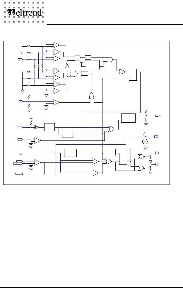
BLOCK DIAGRAM
|
|
- |
|
|
|
|
|
|
|
|
|
[1] |
V33 |
+ UV |
|
|
|
|
|
|
|
|
|
[2] |
V5 |
- UV |
|
|
|
|
|
|
|
|
|
+ |
|
|
|
|
|
|
|
|
|
||
|
|
- UV |
|
UVP |
110us |
|
|
|
|
|
|
[3] |
V12 |
|
|
|
|
|
|
|
|
||
+ |
|
|
|
|
|
|
|
|
|
||
|
|
|
|
|
280ms delay |
|
|
|
|
|
|
|
|
|
|
|
I N |
OUT |
|
|
|
|
|
|
|
-OV |
|
|
CLR |
|
|
|
|
|
|
|
|
|
|
|
|
|
S |
Q |
|
|
|
|
|
+ |
|
|
510us |
|
|
|
|
||
|
|
|
OVP |
|
|
|
|
|
|
||
|
|
-OV |
|
|
|
|
|
|
|
||
|
|
|
|
|
|
|
R |
|
|
|
|
|
|
+ |
|
|
|
|
|
|
|
|
|
|
|
-OV |
|
|
|
|
|
|
|
|
|
|
|
+ |
|
|
|
|
|
|
|
|
|
|
|
-OV |
|
|
|
|
|
|
|
|
|
|
|
+ |
|
|
|
|
|
|
|
|
|
[4] |
PT |
- |
|
|
|
|
|
|
|
|
|
|
|
+ |
|
|
|
|
|
|
|
|
|
|
|
0.62V |
|
|
|
|
|
|
|
|
|
|
|
|
|
|
|
|
|
|
QOUT |
5K |
|
|
|
|
|
|
|
|
|
|
|
|
[11] |
|
|
|
|
|
|
|
280ms delay |
PG |
|
||
|
|
|
|
|
|
|
I N |
|
OUT |
|
|
[9] |
REM |
36mS |
|
REMONF |
|
|
|
|
|
|
|
Delay |
|
|
|
|
|
|
Vss |
|
|||
|
|
|
|
|
|
|
|
||||
|
|
|
|
|
|
|
|
|
|
||
|
|
4.5mS |
|
|
|
|
|
|
|
|
|
|
|
|
REMON |
|
|
|
|
|
|
[10] |
|
|
|
|
Delay |
|
|
|
|
|
|
|
|
|
|
|
|
|
|
|
|
|
SS |
|
|
|
|
- |
|
|
|
|
|
|
|
|
|
[12] |
DET |
|
|
|
|
|
|
|
|
|
|
|
|
+ |
|
|
|
|
|
|
|
|
|
|
|
0.62V |
|
|
|
|
|
|
|
|
|
[6] |
|
|
OSC |
|
|
|
|
|
|
C1 |
[7] |
RT |
|
CLR |
|
|
D |
Q |
|
||||
|
|
PWM CONTROL |
|
|
|
||||||
|
|
|
|
|
|
|
|
||||
|
|
ERROR AMP |
|
|
PWMCMP |
|
|
|
|
|
|
|
|
|
|
- |
|
|
|
|
|
|
|
[16] |
VADJ |
+ |
|
|
|
C |
Q N |
|
|
|
|
|
|
+ |
|
|
|
|
|||||
[15] |
OPNEGIN |
- |
|
|
|
|
|
|
|
|
|
|
|
|
|
|
|
|
C2 |
[8] |
|||
|
|
2.45V |
|
|
|
|
|
|
|
||
|
|
|
|
|
|
|
|
|
|
|
|
|
|
|
|
|
+ |
|
|
|
|
|
|
[14] |
OPOUT |
|
|
|
- |
|
|
|
|
|
|
|
|
|
|
|
DETCMP |
|
|
|
|
|
|
|
|
|
|
|
SOFT_START CONTROLLER |
|
|
|
|
|
|
ABSOLUTE MAXIMUM RATINGS, VCC=5.5V
CHARACTERISTICS |
SYMBOL |
VALUE |
Unit |
|
|
|
|
Supply voltage |
VCC |
5.5 |
V |
Drain output voltage |
Vcc1, Vcc2 |
5.5 |
V |
Drain output current |
Icc1, Icc2 |
200 |
mA |
Power dissipation |
Pd |
200 |
mW |
Operating temperature |
Topr |
-10 ~ +70 |
|
Storage temperature |
Tstg |
-65 ~ +150 |
|
Weltrend Semiconductor, Inc.
Page 4

WT7520
Data Sheet Rev. 0.90
ELECTRICALCHARACTERISTICS,TA=25, VCC=5V,
CHARACTERISTICS |
SYMBOL |
|
TEST CONDITION |
Min. |
Typ. |
Max. |
Unit |
|
|
|
|
|
|
|
|
|
|
|
|
|
|
|
|
DEAD TIME CONTROL SECTION |
|
|
|
|
|
|
|
INPUT THRESHOLD VOLTAGE |
Vthdt |
|
ZERO DUTY CYCLE |
|
3.0 |
3.3 |
V |
|
|
|
MAX. DUTY CYCLE |
|
0.1 |
|
|
ERROR AMP SECTION |
|
|
|
|
|
|
|
CLOSE LOOP VOLTAGE GAIN |
|
|
0.5V ~ 3.5V |
|
65 |
|
dB |
CROSS OVER POINT |
|
|
0dB |
|
320 |
|
KHZ |
OPNEG BIAS VOLTAGE |
|
|
OPNEG OPEN |
2.38 |
2.45 |
2.52 |
V |
OUTPUT SECTION |
|
|
|
|
|
|
|
OUTPUT SATURATION VOLTAGE |
Vdssat |
|
Id=200mA |
|
1.1 |
1.3 |
V |
DRAIN OFF-STATE CURRENT |
Idoff |
|
Vcc=Vd=Vs=0V |
|
2 |
10 |
uA |
RISING TIME |
Tr |
|
|
|
100 |
200 |
ns |
FALLING TIME |
Tf |
|
|
|
50 |
200 |
ns |
PROTECTION SECTION |
|
|
|
|
|
|
|
OVER VOLTAGE PROTECTION OVP V33 |
|
|
3.8 |
4.1 |
4.3 |
V |
|
|
V5 |
|
|
5.8 |
6.2 |
6.6 |
V |
|
V12 |
|
|
4.41 |
4.64 |
4.90 |
V |
|
PT |
|
|
1.2 |
1.25 |
1.3 |
V |
UNDER VOLTAGE PROTECTION V33 |
|
|
1.78 |
1.98 |
2.18 |
V |
|
UVP |
V5 |
|
|
2.70 |
3.00 |
3.30 |
V |
|
V12 |
|
|
2.11 |
2.37 |
2.63 |
V |
UVP DISABLE VOLTAGE |
PT |
|
|
0.55 |
0.62 |
0.68 |
V |
UVP DELAY TIME |
Td.uvp |
|
|
100 |
280 |
500 |
ms |
REMOTE ON/OFF SECTION |
|
|
|
|
|
|
|
REM HIGH INPUT VOLTAGE |
Vremh |
|
|
2.0 |
|
|
V |
REM LOW INPUT VOLTAGE |
Vreml |
|
|
|
|
0.8 |
V |
REM PULL HIGH VOLTAGE |
Vremo |
|
|
2.0 |
|
5.25 |
V |
REM DELAY TIME |
Trem |
|
|
30 |
36 |
42 |
ms |
REM OFF DELAY TIME |
Toff |
|
|
3.5 |
4.5 |
5.5 |
ms |
POWER GOOD SECTION |
|
|
|
|
|
|
|
DETECTING INPUT VOLTAGE |
Vdet |
|
|
0.55 |
0.62 |
0.68 |
V |
PG OUTPUT PULL–UP RESISTOR |
Rpup, pg |
|
|
|
5 |
|
KΩ |
PG OUTPUT LOAD RESISTOR |
Rpg |
|
|
0.5 |
1 |
2 |
KΩ |
PG DELAY TIME |
|
|
|
150 |
280 |
350 |
ms |
OUTPUT SATURATION VOLTAGE |
Vsat.pg |
|
Ipg=10mA |
|
0.2 |
0.4 |
V |
SOFT START SECTION |
|
|
|
|
|
|
|
SINK CURRENT OF SS |
Iss.sink |
|
|
|
13 |
|
uA |
SOURCE CURRENT OF SS |
Iss.source |
|
|
|
700 |
|
uA |
TOTAL DEVICE |
|
|
|
|
|
|
|
STANDBY SUPPLY CURRENT |
Icc |
|
|
|
10 |
20 |
mA |
OSCILLATION SECTION |
|
|
|
|
|
|
|
OSCILLATION FREQUENCY |
Fosc |
|
RT=120KΩ |
50 |
|
70 |
KHZ |
|
|
|
|
|
|
|
|
Weltrend Semiconductor, Inc.
Page 5
WT7520
Data Sheet Rev. 0.90
APPLICATION NOTE
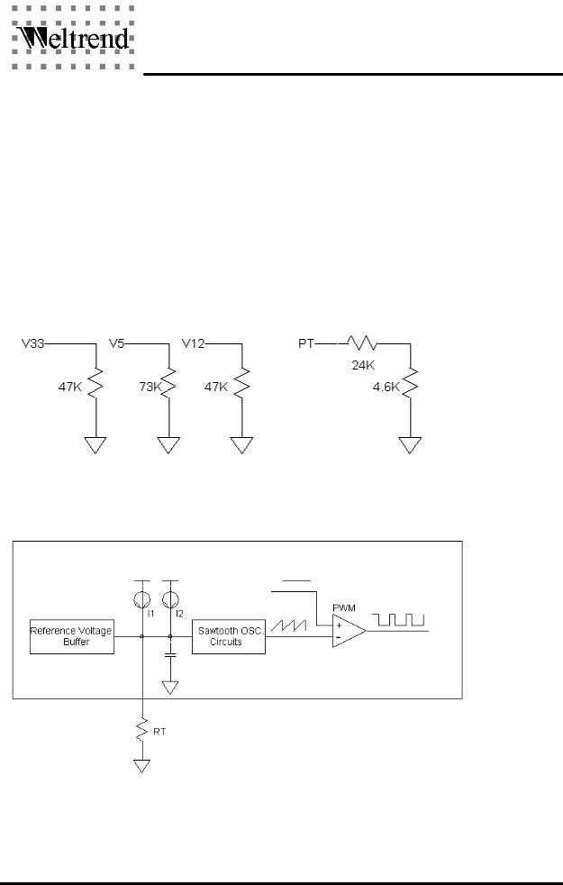
1.Input impedance:
Pin No. |
Pin Name |
Input impedance |
1 |
V33 |
47KΩ |
|
|
|
2 |
V5 |
73KΩ |
|
|
|
3 |
V12 |
47KΩ |
|
|
|
4 |
PT |
24 KΩ+4.6 KΩ |
|
|
|
2.Sawtooth OSC. Funcition:
Weltrend Semiconductor, Inc.
Page 6
WT7520
Data Sheet Rev. 0.90
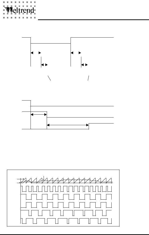
3.REMOTE ON/OFF
REM
REMONF |
|
|
|
|
trem |
|
|
|
trem |
|||||||
|
|
|
|
|
||||||||||||
REMON |
|
|
|
|
|
|
|
|
|
|
|
|
|
|
|
|
|
|
|
|
|
|
|
|
|
|
|
|
|
|
|
||
|
|
|
|
|
|
toff |
|
|
|
|
toff |
|||||
|
|
|
|
|
|
|
|
|
||||||||
SS |
|
|
|
|
|
|
|
|
|
|
|
|
|
|
|
|
|
|
|
|
|
|
|
|
|
|
|
|
|
|
|
|
|
|
|
|
|
|
|
|
|
|
|
|
|
|
|
|
|
|
|
|
|
|
|
|
|
|
|
|
|
|
|
|
|
|
|
4. Under Voltage Protection Delay Time
REM
REMON
td,uvp
UVP
5. Pulse Width Modulation Block
The output pulse width modulation is generated by comparision of the saw–tooth waveform from the capacitor CT to the feedback of the voltage.
Therefore, an increase in feedback control signal amplitude cause a linear decrease of the output pulse width. Also, the SS(DTC and Soft-Start) limits the output pulse width. The timing diagram is shown as below:
PWM OUT
CT
DTC
FF-CLK
FF-Q
FF-QN
C1
C2
Weltrend Semiconductor, Inc.
Page 7
WT7520
Data Sheet Rev. 0.90
6. The function of “PT”:
This signal is prepared for extra OVP/OPP (VPT > 1.25V) or another Disable Under Voltage Protection function (VPT < 0.62V)
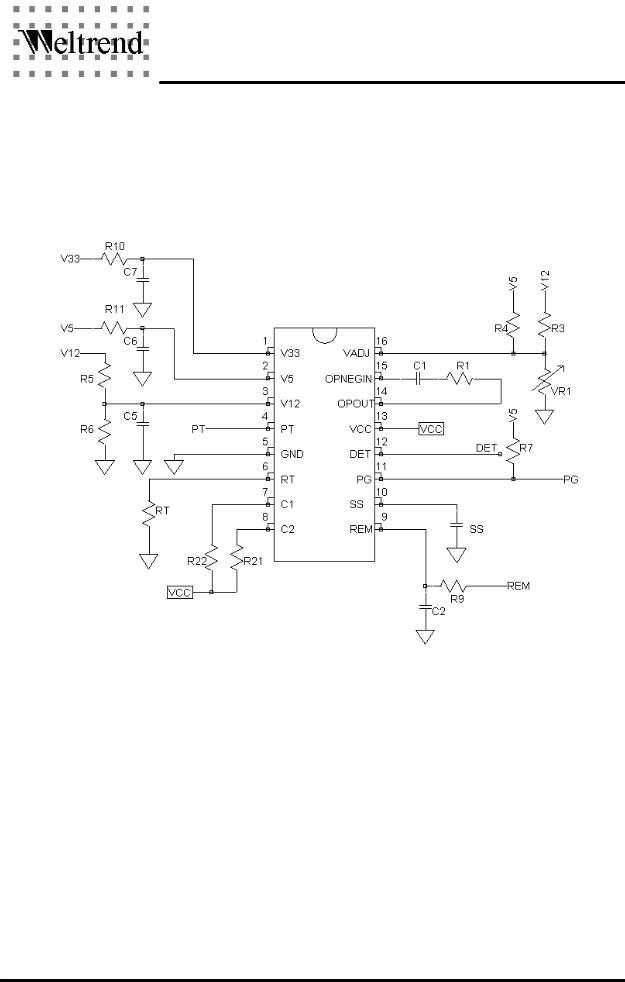
7. Reference Application Ciruit:
8. In some application power system, adding an external resistor (R9) could reduce the peak value spike from the environments to pin 9 (REM) and avoid pin 9 (REM ) damaged by the external noise.
Weltrend Semiconductor, Inc.
Page 8
WT7520
Data Sheet Rev. 0.90
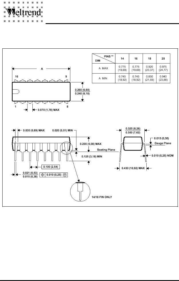
MECHANICAL INFORMATION
PLASTIC DUAL–IN–LINE PACKAGE
NOTE 1 All linear dimensions are in inches millimeters .
NOTE 2 This drawing is subject to change without notice.
NOTE 3 Falls within JEDEC MS–001
Weltrend Semiconductor, Inc.
Page 9