

всё о микросхемах / fn3138
.pdfHIN232, HIN236, HIN237,HIN238,
®
HIN239, HIN240, HIN241
Data Sheet |
August 2002 |
FN3138.12 |
|
|
|
+5V Powered RS-232
Transmitters/Receivers
The HIN232-HIN241 family of RS-232 transmitters/receivers interface circuits meet all ElA RS-232E and V.28 specifications, and are particularly suited for those applications where ±12V is not available. They require a single +5V power supply (except HIN239) and feature onboard charge pump voltage converters which generate +10V and -10V supplies from the 5V supply. The family of devices offer a wide variety of RS-232 transmitter/receiver combinations to accommodate various applications (see Selection Table).
The drivers feature true TTL/CMOS input compatibility, slew- rate-limited output, and 300Ω power-off source impedance. The receivers can handle up to ±30V, and have a 3kΩ to 7kΩ input impedance. The receivers also feature hysteresis to greatly improve noise rejection.
Selection Table
Features
•Meets All RS-232E and V.28 Specifications
•Requires Only Single +5V Power Supply
-(+5V and +12V - HIN239)
•High Data Rate. . . . . . . . . . . . . . . . . . . . . . . . . . . 120kbps
•Onboard Voltage Doubler/Inverter
•Low Power Consumption
•Low Power Shutdown Function
•Three-State TTL/CMOS Receiver Outputs
•Multiple Drivers
-±10V Output Swing for 5V lnput
-300Ω Power-Off Source Impedance
-Output Current Limiting
-TTL/CMOS Compatible
-30V/µs Maximum Slew Rate
•Multiple Receivers
-±30V Input Voltage Range
- |
3kΩ to 7kΩ Input Impedance |
- |
0.5V Hysteresis to Improve Noise Rejection |
Applications
•Any System Requiring RS-232 Communication Ports
-Computer - Portable, Mainframe, Laptop
-Peripheral - Printers and Terminals
-Instrumentation
-Modems
|
|
NUMBER OF |
NUMBER OF |
|
LOW POWER |
|
PART |
POWER SUPPLY |
RS-232 |
RS-232 |
EXTERNAL |
SHUTDOWN/TTL |
NUMBER OF |
NUMBER |
VOLTAGE |
DRIVERS |
RECEIVERS |
COMPONENTS |
THREE-STATE |
LEADS |
|
|
|
|
|
|
|
HIN232 |
+5V |
2 |
2 |
4 Capacitors |
NO/NO |
16 |
|
|
|
|
|
|
|
HIN236 |
+5V |
4 |
3 |
4 Capacitors |
YES/YES |
24 |
|
|
|
|
|
|
|
HIN237 |
+5V |
5 |
3 |
4 Capacitors |
NO/NO |
24 |
|
|
|
|
|
|
|
HIN238 |
+5V |
4 |
4 |
4 Capacitors |
NO/NO |
24 |
|
|
|
|
|
|
|
HIN239 |
+5V and +7.5V to 13.2V |
3 |
5 |
2 Capacitors |
NO/YES |
24 |
|
|
|
|
|
|
|
HIN240 |
+5V |
5 |
5 |
4 Capacitors |
YES/YES |
44 |
|
|
|
|
|
|
|
HIN241 |
+5V |
4 |
5 |
4 Capacitors |
YES/YES |
28 |
|
|
|
|
|
|
|
1 |
CAUTION: These devices are sensitive to electrostatic discharge; follow proper IC Handling Procedures. |
|
1-888-INTERSIL or 321-724-7143 | Intersil (and design) is a trademark of Intersil Americas Inc. |
|
Copyright © Intersil Americas Inc. 2002. All Rights Reserved |

HIN232, HIN236, HIN237, HIN238, HIN239, HIN240, HIN241
Ordering Information
PART |
TEMP. |
|
|
|
NUMBER |
RANGE (oC) |
|
PACKAGE |
PKG. NO. |
HIN232CB |
0 to 70 |
16 Ld SOIC |
M16.3 |
|
|
|
|
|
|
HIN232CB-T |
0 to 70 |
Tape and Reel |
|
|
|
|
|
|
|
HIN232CP |
0 to 70 |
16 Ld PDIP |
E16.3 |
|
|
|
|
|
|
HIN232IB |
-40 to 85 |
16 |
Ld SOIC |
M16.3 |
|
|
|
|
|
HIN232IP |
-40 to 85 |
16 |
Ld PDIP |
E16.3 |
|
|
|
|
|
HIN236CB |
0 to 70 |
24 Ld SOIC |
M24.3 |
|
|
|
|
|
|
HIN236IB |
-40 to 85 |
24 |
Ld SOIC |
M24.3 |
|
|
|
|
|
HIN237CB |
0 to 70 |
24 Ld SOIC |
M24.3 |
|
|
|
|
|
|
HIN237CB-T |
0 to 70 |
Tape and Reel |
|
|
|
|
|
|
|
HIN238CB |
0 to 70 |
24 Ld SOIC |
M24.3 |
|
|
|
|
|
|
Ordering Information |
(Continued) |
|
||
PART |
TEMP. |
|
|
|
NUMBER |
RANGE (oC) |
|
PACKAGE |
PKG. NO. |
HIN238CB-T |
0 to 70 |
Tape and Reel |
|
|
|
|
|
|
|
HIN238CP |
0 to 70 |
24 |
Ld PDIP |
E24.3 |
|
|
|
|
|
HIN238IB |
-40 to 85 |
24 |
Ld SOIC |
M24.3 |
|
|
|
|
|
HIN239CB |
0 to 70 |
24 |
Ld SOIC |
M24.3 |
|
|
|
|
|
HIN239CB-T |
0 to 70 |
Tape and Reel |
|
|
|
|
|
|
|
HIN239CP |
0 to 70 |
24 |
Ld PDIP |
E24.3 |
|
|
|
|
|
HIN240CN |
0 to 70 |
44 Ld MQFP |
Q44.10X10 |
|
|
|
|
|
|
HIN241CA |
0 to 70 |
28 Ld SSOP |
M28.209 |
|
|
|
|
|
|
HIN241CB |
0 to 70 |
28 |
Ld SOIC |
M28.3 |
|
|
|
|
|
HIN241IB |
-40 to 85 |
28 |
Ld SOIC |
M28.3 |
|
|
|
|
|
Pin Descriptions
PIN |
FUNCTION |
||||
|
|
||||
VCC |
Power Supply Input 5V ±10%. |
||||
|
V+ |
Internally generated positive supply (+10V nominal), HIN239 requires +7.5V to +13.2V. |
|||
|
|
|
|||
|
V- |
Internally generated negative supply (-10V nominal). |
|||
|
|
||||
GND |
Ground lead. Connect to 0V. |
||||
|
|
||||
C1+ |
External capacitor (+ terminal) is connected to this lead. |
||||
|
|
||||
C1- |
External capacitor (- terminal) is connected to this lead. |
||||
|
|
||||
C2+ |
External capacitor (+ terminal) is connected to this lead. |
||||
|
|
||||
C2- |
External capacitor (- terminal) is connected to this lead. |
||||
|
|
||||
TIN |
Transmitter Inputs. These leads accept TTL/CMOS levels. An internal 400kΩ pull-up resistor to VCC is connected to each lead. |
||||
TOUT |
Transmitter Outputs. These are RS-232 levels (nominally ±10V). |
||||
RIN |
Receiver Inputs. These inputs accept RS-232 input levels. An internal 5kΩ pull-down resistor to GND is connected to each input. |
||||
ROUT |
Receiver Outputs. These are TTL/CMOS levels. |
||||
|
|
|
Enable input. This is an active low input which enables the receiver outputs. With |
|
= 5V, the receiver outputs are placed |
|
EN |
EN |
|||
|
|
|
in a high impedance state. |
||
|
|
|
|||
|
SD |
Shutdown Input. With SD = 5V, the charge pump is disabled, the receiver outputs are in a high impedance state and the |
|||
|
|
|
transmitters are shut off. |
||
|
|
||||
NC |
No Connect. No connections are made to these leads. |
||||
|
|
|
|
|
|
2

HIN232, HIN236, HIN237, HIN238, HIN239, HIN240, HIN241
Pinouts
HIN232 (PDIP, SOIC) |
HIN236 (SOIC) |
TOP VIEW |
TOP VIEW |
C1+ |
1 |
16 |
VCC |
V+ |
2 |
15 |
GND |
C1- |
3 |
14 |
T1OUT |
C2+ |
4 |
13 |
R1IN |
C2- |
5 |
12 |
R1OUT |
V- |
6 |
11 |
T1IN |
T2OUT |
7 |
10 |
T2IN |
R2IN |
8 |
9 |
R2OUT |
|
|
|
|
+5V |
|
|
|
|
|
|
|
|
+ |
|
|
|
|
|
|
|
|
|
1µF |
16 |
|
|
|
|
|
|
|
|
|
|
|
|
|
|
|
|
1 |
|
|
VCC |
|
|
|
|
NOTE 1 |
|
C1+ |
|
|
|
|
|
+ |
||
NOTE 1 |
+ |
|
+5V TO 10V |
|
|
2 |
|
||
|
|
|
V+ |
|
|||||
3 |
|
VOLTAGE DOUBLER |
|
|
|
||||
|
C1- |
|
|
|
|||||
|
|
|
|
|
|
|
|
|
|
|
4 |
C2+ |
|
|
|
|
|
|
|
NOTE 1 |
+ |
|
+10V TO -10V |
|
V- |
6 |
|
|
|
5 |
|
|
|
|
|||||
|
C2- |
VOLTAGE INVERTER |
|
|
+ NOTE 1 |
||||
|
|
|
|
|
|
|
|||
|
11 |
+5V |
|
T1 |
|
|
14 |
|
|
T1IN |
400kΩ |
|
|
|
|
T1OUT |
|||
|
|
|
|
|
|
|
|
||
|
10 |
+5V |
|
T2 |
|
|
7 |
|
|
T2IN |
400kΩ |
|
|
|
|
T2OUT |
|||
|
|
|
|
|
|
|
|
||
R1OUT |
12 |
|
|
|
|
|
13 |
|
R1IN |
|
|
|
|
5kΩ |
|
|
|
||
|
|
|
|
R1 |
|
|
|
|
|
R2OUT |
9 |
|
|
|
|
|
8 |
|
R2IN |
|
|
|
|
5kΩ |
|
|
|
||
|
|
|
|
R2 |
|
|
|
|
|
|
|
|
|
15 |
|
|
|
|
|
NOTE: |
|
|
|
|
|
|
|
|
|
1.Either 0.1 F or 1 F capacitors may be used. The V+ capacitor may be terminated to VCC or to GND.
|
T3OUT |
1 |
|
24 |
T4OUT |
|
||
|
T1OUT |
2 |
|
23 |
R2IN |
|
|
|
|
T2OUT |
3 |
|
22 |
R2OUT |
|
||
|
|
R1IN |
4 |
|
21 |
SD |
|
|
|
R1OUT |
5 |
|
20 |
EN |
|
|
|
|
|
T2IN |
6 |
|
19 |
T4IN |
|
|
|
|
T1IN |
7 |
|
18 |
T3IN |
|
|
|
|
GND |
8 |
|
17 |
R3OUT |
|
|
|
|
VCC |
9 |
|
16 |
R3IN |
|
|
|
|
C1+ |
10 |
|
15 |
V- |
|
|
|
|
V+ |
11 |
|
14 |
C2- |
|
|
|
|
C1- |
12 |
|
13 |
C2+ |
|
|
|
|
|
|
+5V |
|
|
|
|
|
10 |
|
|
9 |
|
|
|
1µF |
|
C1+ |
|
VCC |
|
|
|
||
|
|
|
|
11 |
+ |
|||
1µF |
+ |
|
|
+5V TO 10V |
|
V+ |
|
|
|
12 |
C1- |
|
|
|
|
|
|
|
VOLTAGE DOUBLER |
|
|
|
||||
|
13 |
C2+ |
|
|
|
|
|
|
1µF |
+ |
|
|
+10V TO -10V |
|
V- |
15 |
|
14 |
|
|
|
|
||||
|
C2- |
VOLTAGE INVERTER |
|
|
+1µF |
|||
|
|
|
T1 |
|
|
|
||
|
7 |
+5V |
400kΩ |
|
|
2 |
|
|
T1IN |
|
|
|
|
T1OUT |
|||
|
|
|
|
|
|
|
||
|
6 |
+5V |
400kΩ |
T2 |
|
|
3 |
|
T2IN |
|
|
|
|
T2OUT |
|||
|
|
|
|
|
|
|
||
|
18 |
+5V |
400kΩ |
T3 |
|
|
1 |
|
T3IN |
|
|
|
|
T3OUT |
|||
|
|
|
|
|
|
|
||
|
19 |
+5V |
400kΩ |
T4 |
|
|
24 |
|
T4IN |
|
|
|
|
T4OUT |
|||
5 |
|
|
|
|
|
4 |
||
R1OUT |
|
|
|
|
|
R1IN |
||
|
|
|
|
5kΩ |
|
|
||
|
|
|
|
R1 |
|
|
|
|
R2OUT |
22 |
|
|
|
|
|
23 |
R2IN |
|
|
|
|
5kΩ |
|
|
||
|
|
|
|
R2 |
|
|
|
|
R3OUT |
17 |
|
|
|
|
|
16 |
R3IN |
|
|
|
|
5kΩ |
|
21 |
||
EN |
20 |
|
|
R3 |
|
SD |
||
|
|
|
|
|
|
|
||
|
|
|
|
8 |
|
|
|
|
3

HIN232, HIN236, HIN237, HIN238, HIN239, HIN240, HIN241
Pinouts (Continued)
HIN237 (SOIC) |
HIN238 (PDIP, SOIC) |
TOP VIEW |
TOP VIEW |
|
|
T3OUT |
|
1 |
|
24 |
T4OUT |
|
|
|
T2OUT |
1 |
|
|
24 |
T3OUT |
|
||
|
|
T1OUT |
|
2 |
|
23 |
R2IN |
|
|
|
|
|
|
||||||
|
|
T2OUT |
|
3 |
|
22 |
R2OUT |
|
|
|
T1OUT |
2 |
|
|
23 |
R3IN |
|
||
|
|
R1IN |
|
4 |
|
21 |
T5IN |
|
|
|
R2IN |
3 |
|
|
22 |
R3OUT |
|
||
|
|
R1OUT |
|
5 |
|
20 |
T5OUT |
|
|
R2OUT |
4 |
|
|
21 |
T4IN |
|
|||
|
|
T2IN |
|
6 |
|
19 |
T4IN |
|
|
|
T1IN |
5 |
|
|
20 |
T4OUT |
|
||
|
|
T1IN |
|
7 |
|
18 |
T3IN |
|
|
R1OUT |
6 |
|
|
19 |
T3IN |
|
|||
|
|
GND |
|
8 |
|
17 |
R3OUT |
|
|
|
R1IN |
7 |
|
|
18 |
T2IN |
|
||
|
|
VCC |
|
9 |
|
16 |
R3IN |
|
|
|
GND |
8 |
|
|
17 |
R4OUT |
|
||
|
|
C1+ |
10 |
|
15 |
V- |
|
|
|
VCC |
9 |
|
|
16 |
R4IN |
|
|||
|
|
|
V+ |
11 |
|
14 |
C2- |
|
|
|
C1+ |
10 |
|
|
15 |
V- |
|
|
|
|
|
|
C1- |
12 |
|
13 |
C2+ |
|
|
|
V+ |
11 |
|
|
14 |
C2- |
|
|
|
|
|
|
|
|
|
|
|
|
|
|
|
C1- |
12 |
|
|
13 |
C2+ |
|
|
|
|
|
|
|
+5V |
|
|
|
|
|
|
|
|
+5V |
|
|
|
|
|
|
|
|
|
|
9 |
|
|
|
|
|
|
|
|
|
|
|
|
|
|
|
10 |
|
|
|
|
|
|
1µF |
|
|
|
|
|
9 |
|
|
|
1µF |
|
|
C1+ |
|
|
VCC |
|
|
|
|
10 |
|
|
|
|
|
|
||||
|
|
|
|
|
|
|
|
|
V |
|
|
|
|
||||||
|
+ |
|
|
|
|
11 |
+ |
|
C1+ |
|
CC |
|
|
11 |
+ |
||||
1µF |
|
|
|
+5V TO 10V |
|
V+ |
|
1µF |
+ |
|
|
|
V+ |
|
|||||
|
12 |
C1- |
|
|
|
|
|
|
12 |
|
|
+5V TO 10V |
|
|
|
||||
|
VOLTAGE DOUBLER |
|
|
|
C1- |
|
|
|
|
||||||||||
|
13 |
C2+ |
|
|
|
|
|
|
|
|
13 |
VOLTAGE DOUBLER |
|
|
|
||||
|
|
|
+10V TO -10V |
|
|
|
|
|
C2+ |
|
|
|
|
|
|
|
|||
1µF |
+ |
|
|
|
|
V- |
15 |
|
1µF |
+ |
|
+10V TO -10V |
|
|
15 |
|
|||
14 |
|
VOLTAGE INVERTER |
+1µF |
|
|
|
V- |
|
|||||||||||
|
|
C2- |
|
|
|
|
|
|
|
14 |
C2- |
VOLTAGE INVERTER |
|
|
1µF |
||||
|
7 |
+5V |
400kΩ |
T1 |
|
|
2 |
|
|
|
+5V |
|
T1 |
|
|
|
2 |
+ |
|
|
|
|
|
|
|
|
|
|
|
|
|
|
|||||||
T1IN |
|
|
|
|
|
|
|
|
T1OUT |
T1IN |
5 |
400kΩ |
|
|
|
|
T1OUT |
||
|
|
|
|
|
|
|
|
|
|
|
|
|
|
|
|||||
|
6 |
+5V |
400kΩ |
T2 |
|
|
3 |
|
|
|
+5V |
|
T2 |
|
|
|
|
|
|
T2IN |
|
|
|
|
T2OUT |
T2IN |
18 |
400kΩ |
|
|
|
|
1 |
T2OUT |
|||||
|
|
|
|
|
|
|
|
|
|
|
|
||||||||
|
18 |
+5V |
400kΩ |
T3 |
|
|
1 |
|
|
|
+5V |
|
T3 |
|
|
|
|
||
|
|
|
|
|
|
|
19 |
|
|
|
24 |
|
|||||||
T3IN |
|
|
|
|
|
|
|
|
T3OUT |
T3IN |
400kΩ |
|
|
|
|
T3OUT |
|||
|
+5V |
|
|
T4 |
|
|
|
|
|
|
|
|
|
|
|
||||
|
19 |
400kΩ |
|
|
24 |
|
|
|
+5V |
|
T4 |
|
|
|
|
||||
|
|
|
|
|
|
|
|
|
|
|
|
|
|||||||
T4IN |
|
|
|
|
T4OUT |
T4IN |
21 |
400kΩ |
|
|
|
|
20 |
T4OUT |
|||||
|
|
|
|
|
|
|
|
|
|
|
|
||||||||
|
+5V |
|
|
T5 |
|
|
|
|
|
|
|
|
|
||||||
T5IN |
21 |
400kΩ |
|
|
20 |
T5OUT |
R1OUT |
6 |
|
|
|
|
|
|
7 |
R1IN |
|||
|
|
|
|
|
|
|
|
|
|
|
|
||||||||
|
|
|
|
|
|
|
|
|
|
|
R1 |
5kΩ |
|
|
|||||
|
5 |
|
|
|
|
|
|
4 |
R1IN |
|
|
|
|
|
|
|
|||
R1OUT |
|
|
|
|
|
|
|
|
|
|
|
|
|
|
|
|
|||
|
|
|
|
|
5kΩ |
|
|
|
4 |
|
|
|
|
|
|
3 |
|
||
|
|
|
|
|
R1 |
|
|
|
R2OUT |
|
|
|
|
|
|
R2IN |
|||
|
|
|
|
|
|
|
|
|
|
|
|
|
5kΩ |
|
|
||||
|
22 |
|
|
|
|
|
|
23 |
R2IN |
|
|
|
|
R2 |
|
|
|
||
R2OUT |
|
|
|
|
|
|
|
|
|
|
|
|
|
|
|
|
|||
|
|
|
|
|
5kΩ |
|
|
|
22 |
|
|
|
|
|
|
23 |
|
||
|
|
|
|
|
R2 |
|
|
|
R3OUT |
|
|
|
|
|
|
R3IN |
|||
|
|
|
|
|
|
|
|
|
|
|
|
|
5kΩ |
|
|
||||
|
17 |
|
|
|
|
|
|
16 |
|
|
|
|
|
R3 |
|
|
|
||
R3OUT |
|
|
|
|
|
|
R3IN |
|
17 |
|
|
|
|
|
|
16 |
|
||
|
|
|
|
R3 |
5kΩ |
|
|
R4OUT |
|
|
|
|
|
|
R4IN |
||||
|
|
|
|
|
|
|
|
|
|
|
R4 |
5kΩ |
|
|
|||||
|
|
|
|
|
|
|
|
|
|
|
|
|
|
|
|
|
|||
|
|
|
|
|
8 |
|
|
|
|
|
|
|
|
|
8 |
|
|
|
|
|
|
|
|
|
|
|
|
|
|
|
|
|
|
|
|
|
|
|
|
|
|
|
|
|
4 |
|
|
|
|
|
|
|
|
|
|
|
|
|
|

HIN232, HIN236, HIN237, HIN238, HIN239, HIN240, HIN241
Pinouts (Continued)
HIN239 (PDIP, SOIC) |
HIN240 (MQFP) |
|
|
|
|
TOP VIEW |
|
|
|
|
|
|
|
|
|
OUT |
IN |
OUT |
|
|
OUT |
IN |
|
|
||
|
|
|
|
|
|
|
|
|
|
|
|
NC SD |
EN |
IN |
IN |
NC |
|
|||||||
|
|
|
|
|
|
|
|
|
|
|
|
T5 |
R4 |
R4 |
T4 |
T3 |
R5 |
R5 |
|
|
||||
|
R1OUT |
1 |
|
|
24 T1IN |
|
|
|
|
|
|
|
|
|
|
|
|
|
|
|
|
|
||
|
|
R1IN |
2 |
|
|
23 T2IN |
|
|
|
|
|
|
|
|
|
|
|
|
|
|
|
|
|
|
|
|
GND |
3 |
|
|
22 R2OUT |
|
NC |
|
1 |
44 43 42 41 40 |
39 38 |
37 36 |
35 34 |
NC |
|||||||||
|
|
VCC |
4 |
|
|
21 R2IN |
|
|
|
|
|
|
|
|
|
|
|
|
|
33 |
||||
|
|
|
|
|
|
T5IN |
|
2 |
|
|
|
|
|
|
|
|
|
32 |
NC |
|||||
|
|
V+ |
5 |
|
|
20 T2OUT |
|
R3OUT |
|
3 |
|
|
|
|
|
|
|
|
|
31 |
NC |
|||
|
|
C1+ |
6 |
|
|
19 T1OUT |
|
R3IN |
|
4 |
|
|
|
|
|
|
|
|
|
30 |
V- |
|||
|
|
C1- |
7 |
|
|
18 |
R3IN |
|
|
T4OUT |
|
5 |
|
|
|
|
|
|
|
|
|
29 |
C2- |
|
|
|
V- |
8 |
|
|
17 R3OUT |
|
T3OUT |
|
6 |
|
|
|
|
|
|
|
|
|
28 |
C2+ |
|||
|
|
R5IN |
9 |
|
|
16 T3IN |
|
|
T1OUT |
|
7 |
|
|
|
|
|
|
|
|
|
27 |
C1- |
||
|
R5OUT 10 |
|
|
15 NC |
|
|
T2OUT |
|
8 |
|
|
|
|
|
|
|
|
|
26 |
V+ |
||||
|
|
|
|
|
NC |
|
9 |
|
|
|
|
|
|
|
|
|
25 |
C1+ |
||||||
|
R4OUT 11 |
|
|
14 EN |
|
|
|
|
|
|
|
|
|
|
|
|
||||||||
|
|
|
|
|
R2IN |
|
10 |
|
|
|
|
|
|
|
|
|
24 |
NC |
||||||
|
|
R4IN |
12 |
|
|
13 T3OUT |
|
|
|
|
|
|
|
|
|
|
|
|||||||
|
|
|
|
|
NC |
|
11 |
|
|
|
17 |
18 |
19 |
|
|
|
23 |
NC |
||||||
|
|
|
|
|
|
|
|
|
|
|
|
12 13 14 15 16 |
20 21 22 |
|
||||||||||
|
|
|
|
|
|
|
|
|
|
|
|
|
OUT |
IN |
IN |
OUT |
IN |
GND |
CC |
NC |
NC |
|
NC |
|
|
|
|
|
|
|
|
|
|
|
|
|
NC R2 |
T2 |
T1 |
R1 |
R1 |
V |
|
|
|||||
|
|
|
|
+5V |
+7.5V TO +13.2V (NOTE) |
|
|
|
|
|
+5V |
19 |
|
|
|
|
|
|
|
|||||
|
|
|
|
|
25 |
|
|
|
|
|
|
|
|
|
|
|
1µF |
|||||||
|
|
|
|
|
4 |
|
|
|
|
|
C1+ |
|
|
VCC |
|
|
|
|
|
26 |
||||
|
6 |
|
|
|
|
|
|
|
1µF |
+ |
|
|
|
|
V+ |
|
+ |
|||||||
|
C1+ |
|
|
VCC |
|
|
|
|
27 |
C1- |
|
+5V TO 10V |
|
|
|
|
||||||||
1µF |
+ 7 |
|
|
|
V+ |
5 |
|
|
VOLTAGE DOUBLER |
|
|
|
|
|
||||||||||
C1- |
|
+10V TO -10V |
|
|
|
28 |
C2+ |
|
+10V TO -10V |
|
|
|
|
|
|
|||||||||
(NOTE) |
|
VOLTAGE INVERTER |
V- |
8 |
|
1µF |
+ |
|
|
|
|
V- |
|
30 |
|
|||||||||
|
|
|
|
|
|
|
1µF |
29 |
C2- |
VOLTAGE INVERTER |
|
1µF |
||||||||||||
|
|
+5V |
|
T1 |
|
|
|
+ |
|
|
|
+5V |
|
|
T1 |
|
|
|
|
|
|
|
||
|
24 |
400kΩ |
|
|
19 |
|
|
15 |
|
|
|
|
|
|
|
|
7 |
|
||||||
T1IN |
|
|
|
|
|
T1OUT |
T1IN |
|
400kΩ |
|
|
|
|
|
|
|
T1OUT |
|||||||
|
|
|
|
|
|
|
|
|
|
|
|
|
|
|
|
|
|
|
|
|
||||
|
|
+5V |
|
|
T2 |
|
|
|
|
|
|
|
+5V |
|
|
T2 |
|
|
|
|
|
|
|
|
|
23 |
400kΩ |
|
|
|
20 |
|
T2IN |
14 |
|
400kΩ |
|
|
|
|
|
|
|
8 |
T2OUT |
||||
T2IN |
|
|
|
|
|
T2OUT |
|
|
|
|
|
|
|
|
||||||||||
|
|
|
|
|
|
|
|
|
|
|
|
|
|
|
|
|
|
|||||||
|
|
|
|
|
|
|
|
|
|
+5V |
|
|
|
|
|
|
|
|
|
|
||||
|
|
+5V |
|
|
T3 |
|
|
|
|
|
37 |
|
|
|
T3 |
|
|
|
|
|
6 |
|
||
T3IN |
16 |
400kΩ |
|
|
|
13 |
T3OUT |
T3IN |
|
400kΩ |
|
|
|
|
|
|
|
T3OUT |
||||||
|
|
|
|
|
|
|
|
|
|
|
|
|
|
|
|
|
|
|||||||
|
|
|
|
|
|
|
|
+5V |
|
|
T4 |
|
|
|
|
|
|
|
||||||
|
1 |
|
|
|
|
|
|
2 |
|
|
38 |
|
|
|
|
|
|
|
|
5 |
|
|||
R1OUT |
|
|
|
|
|
|
R1IN |
T4IN |
|
400kΩ |
|
|
|
|
|
|
|
T4OUT |
||||||
|
|
|
|
R1 |
5kΩ |
|
|
|
|
|
|
|
|
|
|
|
|
|
|
|
||||
|
|
|
|
|
|
|
|
|
|
|
+5V |
|
|
T5 |
|
|
|
|
|
|
|
|
||
|
|
|
|
|
|
|
|
|
|
2 |
|
|
|
|
|
|
|
|
41 |
|
||||
|
22 |
|
|
|
|
|
|
21 |
|
T5IN |
|
400kΩ |
|
|
|
|
|
|
|
T5OUT |
||||
R2OUT |
|
|
|
|
|
|
R2IN |
16 |
|
|
|
|
|
|
|
|
|
|
17 |
|||||
|
|
|
|
R2 |
5kΩ |
|
|
R1OUT |
|
|
|
|
|
|
|
|
|
|
R1IN |
|||||
|
|
|
|
|
|
|
|
|
|
|
|
|
R1 |
|
5kΩ |
|
|
|
|
|||||
|
17 |
|
|
|
|
|
|
18 |
|
|
|
|
|
|
|
|
|
|
|
|
|
|||
R3OUT |
|
|
|
|
|
|
R3IN |
|
13 |
|
|
|
|
|
|
|
|
|
|
10 |
|
|||
|
|
|
|
|
|
|
|
R2OUT |
|
|
|
|
|
|
|
|
|
|
R2IN |
|||||
|
|
|
|
R3 |
5kΩ |
|
|
|
|
|
|
|
|
|
|
5kΩ |
|
|
|
|
||||
|
|
|
|
|
|
|
|
|
|
|
|
|
|
R2 |
|
|
|
|
|
|
||||
|
|
|
|
|
|
|
|
|
|
|
|
|
|
|
|
|
|
|
|
|
||||
R4OUT |
11 |
|
|
|
|
|
|
12 |
R4IN |
R3OUT |
3 |
|
|
|
|
|
|
|
|
|
|
4 |
R3IN |
|
|
|
|
|
R4 |
5kΩ |
|
|
|
|
|
|
|
|
|
|
5kΩ |
|
|
|
|
||||
|
|
|
|
|
|
|
|
|
|
|
|
|
|
R3 |
|
|
|
|
|
|
||||
|
10 |
|
|
|
|
|
|
9 |
R5IN |
R4OUT |
39 |
|
|
|
|
|
|
|
|
|
|
40 |
R4IN |
|
R5OUT |
|
|
|
|
|
|
|
|
|
|
|
|
|
|
|
|
|
|
|
|||||
|
|
|
|
|
5kΩ |
|
|
|
|
|
|
|
R4 |
|
5kΩ |
|
|
|
|
|||||
|
14 |
|
|
|
R5 |
|
|
|
|
36 |
|
|
|
|
|
|
|
35 |
|
|||||
EN |
|
|
|
|
|
|
|
|
|
|
|
|
|
|
|
|
|
|
|
|
||||
|
|
|
|
|
|
|
|
|
R5OUT |
|
|
|
|
|
|
|
|
|
|
R5IN |
||||
|
|
|
|
|
|
|
|
|
|
|
|
|
|
|
|
|
|
5kΩ |
|
|
|
|
||
|
|
|
|
|
3 |
|
|
|
|
EN |
42 |
|
|
|
|
R5 |
|
|
|
43 SD |
||||
|
|
|
|
|
|
|
|
|
|
|
|
|
|
|
|
|
|
|
|
|||||
NOTE: For V+ > 11V, use C1 ≤ |
0.1 F. |
|
|
|
|
|
|
|
|
|
|
|
18 |
|
|
|
|
|
|
|
||||
|
|
|
|
|
5 |
|
|
|
|
|
|
|
|
|
|
|
|
|
|
|
|
|
|
|

HIN232, HIN236, HIN237, HIN238, HIN239, HIN240, HIN241
Pinouts (Continued)
|
|
|
HIN241 (SOIC, SSOP) |
|
|
|
|||
|
|
|
|
TOP VIEW |
|
|
|
|
|
|
T3OUT |
1 |
|
|
28 |
T4OUT |
|||
|
T1OUT |
2 |
|
|
27 |
R3IN |
|
||
|
T2OUT |
3 |
|
|
26 |
R3OUT |
|||
|
|
R2IN |
4 |
|
|
25 |
SD |
|
|
|
R2OUT |
5 |
|
|
24 |
EN |
|
||
|
|
T2IN |
6 |
|
|
23 |
R4IN |
|
|
|
|
T1IN |
7 |
|
|
22 |
R4OUT |
||
|
R1OUT |
8 |
|
|
21 |
T4IN |
|
||
|
|
R1IN |
9 |
|
|
20 |
T3IN |
|
|
|
|
GND 10 |
|
|
19 |
R5OUT |
|||
|
|
VCC |
11 |
|
|
18 |
R5IN |
|
|
|
|
C1+ |
12 |
|
|
17 |
V- |
|
|
|
|
V+ |
13 |
|
|
16 |
C2- |
|
|
|
|
C1- |
14 |
|
|
15 |
C2+ |
|
|
|
|
|
|
+5V |
|
|
|
|
|
|
12 |
|
|
11 |
|
|
|
|
1µF |
|
C1+ |
|
VCC |
|
|
|
13 |
||
|
|
|
|
|
+ |
||||
1µF |
+ |
C1- |
|
+5V TO 10V |
|
V+ |
|
|
|
|
14 |
VOLTAGE DOUBLER |
|
|
|
|
|||
|
15 |
C2+ |
|
|
|
|
|
|
|
1µF |
+ |
|
+10V TO -10V |
|
V- |
17 |
|
||
|
|
|
|
||||||
|
16 |
C2- |
VOLTAGE INVERTER |
|
|
|
+1µF |
||
|
|
|
|
|
|
|
|
||
|
|
+5V |
|
T1 |
|
|
|
|
|
|
7 |
|
|
|
|
2 |
|
||
T1IN |
400kΩ |
|
|
|
|
T1OUT |
|||
|
|
|
|
|
|
|
|
||
|
6 |
+5V |
|
T2 |
|
|
|
3 |
|
T2IN |
400kΩ |
|
|
|
|
T2OUT |
|||
|
|
|
|
|
|
|
|
||
|
20 |
+5V |
|
T3 |
|
|
|
1 |
|
T3IN |
400kΩ |
|
|
|
|
T3OUT |
|||
|
|
|
|
|
|
|
|
||
|
21 |
+5V |
|
T4 |
|
|
|
28 |
|
T4IN |
400kΩ |
|
|
|
|
T4OUT |
|||
8 |
|
|
|
|
|
|
9 |
||
R1OUT |
|
|
|
|
|
|
R1IN |
||
|
|
|
|
5kΩ |
|
|
|
||
|
|
|
|
R1 |
|
|
|
|
|
R2OUT |
5 |
|
|
|
|
|
|
4 |
R2IN |
|
|
|
|
5kΩ |
|
|
|
||
|
|
|
|
R2 |
|
|
|
|
|
R3OUT |
26 |
|
|
|
|
|
|
27 |
R3IN |
|
|
|
|
5kΩ |
|
|
|
||
|
|
|
|
R3 |
|
|
|
|
|
R4OUT |
22 |
|
|
|
|
|
|
23 |
R4IN |
|
|
|
|
5kΩ |
|
|
|
||
|
|
|
|
R4 |
|
|
|
|
|
R5OUT |
19 |
|
|
|
|
|
|
18 |
R5IN |
|
|
|
|
5kΩ |
|
|
|
||
|
24 |
|
|
R5 |
|
|
25 |
|
|
EN |
|
|
|
|
|
|
SD |
||
|
|
|
|
10 |
|
|
|
|
|
6

HIN232, HIN236, HIN237, HIN238, HIN239, HIN240, HIN241
Absolute Maximum Ratings |
Thermal Information |
VCC to Ground. . . . . . . . . . . . . . . . . . . . . . (GND -0.3V) < VCC < 6V V+ to Ground (Note 2) . . . . . . . . . . . . . . . (VCC -0.3V) < V+ < 13.2V V- to Ground. . . . . . . . . . . . . . . . . . . . . . . . -12V < V- < (GND +0.3V)
V+ to V- . . . . . . . . . . . . . . . . . . . . . . . . . . . . . . . . . . . . . . . . . . . 24V Input Voltages
TIN . . . . . . . . . . . . . . . . . . . . . . . . . . . . . -0.3V < VIN < (V+ +0.3V) RIN . . . . . . . . . . . . . . . . . . . . . . . . . . . . . . . . . . . . . . . . . . . . ±30V
Output Voltages
TOUT . . . . . . . . . . . . . . . . . . . .(V- -0.3V) < VTXOUT < (V+ +0.3V) ROUT . . . . . . . . . . . . . . . . . (GND -0.3V) < VRXOUT < (V+ +0.3V)
Short Circuit Duration
TOUT . . . . . . . . . . . . . . . . . . . . . . . . . . . . . . . . . . . . . .Continuous ROUT . . . . . . . . . . . . . . . . . . . . . . . . . . . . . . . . . . . . . .Continuous
Thermal Resistance (Typical, Note 3) |
θ JA (oC/W) |
16 Ld PDIP Package . . . . . . . . . . . . . . . . . . . . . . |
. . 90 |
24 Ld PDIP Package . . . . . . . . . . . . . . . . . . . . . . . |
. 70 |
16 Ld SOIC Package . . . . . . . . . . . . . . . . . . . . . . . |
. 100 |
24 Ld SOIC Package . . . . . . . . . . . . . . . . . . . . . . . |
. 75 |
28 Ld SOIC Package . . . . . . . . . . . . . . . . . . . . . . . |
. 70 |
28 Ld SSOP Package . . . . . . . . . . . . . . . . . . . . . . |
. 95 |
44 Ld MQFP Package . . . . . . . . . . . . . . . . . . . . . . |
. 80 |
Maximum Junction Temperature (Plastic Package) . |
. . . . . . .150oC |
Maximum Storage Temperature Range . . . . . . . . . . |
-65oC to 150oC |
Maximum Lead Temperature (Soldering 10s) . . . . . . |
. . . . . . .300oC |
(SOIC, SSOP, MQFP - Lead Tips Only) |
|
Operating Conditions
Temperature Range
HIN2XXCX . . . . . . . . . . . . . . . . . . . . . . . . . . . . . . . . . 0oC to 70oC
HIN2XXIX . . . . . . . . . . . . . . . . . . . . . . . . . . . . . . . . -40oC to 85oC
CAUTION: Stresses above those listed in “Absolute Maximum Ratings” may cause permanent damage to the device. This is a stress only rating and operation of the device at these or any other conditions above those indicated in the operational sections of this specification is not implied.
NOTE:
2.Only HIN239. For V+ > 11V, C1 must be ≤ 0.1µF.
3.θ JA is measured with the component mounted on a low effective thermal conductivity test board in free air. See Tech Brief TB379 for details.
Electrical Specifications Test Conditions: VCC = +5V ±10%, TA = Operating Temperature Range
PARAMETER |
|
|
|
|
|
TEST CONDITIONS |
MIN |
TYP |
MAX |
UNITS |
||
|
|
|
|
|
|
|
|
|
|
|
|
|
SUPPLY CURRENTS |
|
|
|
|
|
|
|
|
|
|
|
|
|
|
|
|
|
|
|
|
|
|
|||
Power Supply Current, ICC |
|
|
|
No Load, |
HIN232 |
- |
5 |
10 |
mA |
|||
|
|
|
|
T = 25oC |
|
|
|
|
|
|||
|
|
|
|
|
|
|
|
|
||||
|
|
|
|
A |
HIN236-238, HIN240-241 |
- |
7 |
15 |
mA |
|||
|
|
|
|
|
|
|
|
|||||
|
|
|
|
|
|
|
|
|
|
|
|
|
|
|
|
|
|
|
|
|
HIN239 |
- |
0.4 |
1 |
mA |
|
|
|
|
|
|
|
|
|
||||
V+ Power Supply Current, ICC |
|
|
No Load, |
HIN239 |
- |
5.0 |
15 |
mA |
||||
No Load, TA = 25oC |
|
|
|
TA = 25oC |
|
|
|
|
|
|||
Shutdown Supply Current, I |
CC |
(SD) |
|
T = 25oC |
|
- |
1 |
10 |
µA |
|||
|
|
|
A |
|
|
|
|
|
||||
LOGIC AND TRANSMITTER INPUTS, RECEIVER OUTPUTS |
|
|
|
|
|
|||||||
|
|
|
|
|
|
|
|
|
|
|
|
|
Input Logic Low, VlL |
|
|
|
TIN, |
|
Shutdown |
- |
- |
0.8 |
V |
||
|
|
EN, |
||||||||||
Input Logic High, VlH |
|
|
|
TIN |
|
2.0 |
- |
- |
V |
|||
|
|
|
|
|
Shutdown |
|
2.4 |
- |
- |
V |
||
|
|
|
|
EN, |
|
|||||||
|
|
|
|
|
|
|
|
|||||
Transmitter Input Pullup Current, IP |
|
TIN = 0V |
|
- |
15 |
200 |
µA |
|||||
TTL/CMOS Receiver Output Voltage Low, VOL |
|
IOUT = 1.6mA |
|
- |
0.1 |
0.4 |
V |
|||||
TTL/CMOS Receiver Output Voltage High, VOH |
|
IOUT = -1.0mA |
|
3.5 |
4.6 |
- |
V |
|||||
RECEIVER INPUTS |
|
|
|
|
|
|
|
|
|
|
|
|
|
|
|
|
|
|
|
|
|
|
|
||
RS-232 Input Voltage Range VIN |
|
|
|
|
|
|
-30 |
- |
+30 |
V |
||
Receiver Input Impedance RIN |
|
VIN = ±3V |
|
3.0 |
5.0 |
7.0 |
kΩ |
|||||
Receiver Input Low Threshold, VlN (H-L) |
|
VCC = 5V, TA = 25oC |
0.8 |
1.2 |
- |
V |
||||||
Receiver Input High Threshold, VIN (L-H) |
|
VCC = 5V, TA = 25oC |
- |
1.7 |
2.4 |
V |
||||||
Receiver Input Hysteresis VHYST |
|
|
|
|
|
|
0.2 |
0.5 |
1.0 |
V |
||
TIMING CHARACTERISTICS |
|
|
|
|
|
|
|
|
|
|
|
|
|
|
|
|
|
|
|
||||||
Baud Rate (1 Transmitter Switching) |
RL = 3kΩ |
|
120 |
- |
- |
kbps |
||||||
7

HIN232, HIN236, HIN237, HIN238, HIN239, HIN240, HIN241
Electrical Specifications |
Test Conditions: VCC = +5V ±10%, TA = Operating Temperature Range (Continued) |
|
|
|
|
|||||||||||||||||||||||||||||||||||||||||||||||||||||||||||||||||||||||||||||||||||||||||||||||||||||
|
|
|
PARAMETER |
|
|
|
|
|
|
|
|
|
|
|
|
|
|
|
|
|
|
|
|
|
|
|
|
|
|
|
|
|
|
|
|
|
|
|
|
|
TEST CONDITIONS |
|
|
|
|
|
|
|
|
|
|
|
|
|
|
|
|
|
|
|
|
MIN |
|
|
TYP |
MAX |
UNITS |
|||||||||||||||||||||||||||||||||||||||
|
|
|
|
|
|
|
|
|
|
|
|
|
|
|
|
|
|
|
|
|
|
|
|
|
|
|
|
|
|
|
|
|
|
|
|
|
|
|
|
|
|
|
|
|
|
|
|
|
|
|
|
|
|
|
|
|
|
|
|
|
|
|
|
|
|
|
|
|
|
|
|
|
|
|
|
|
|
|
|
|
|
|
|
|
|
|
|
|
|
|
|
|
|
|
|
|
|
|
|
|
|
|
|
|
|
|
Output Enable Time, tEN |
|
|
|
|
|
|
|
|
|
|
|
|
|
|
|
|
|
|
|
|
|
HIN236, 239, 240, 241 |
|
|
|
|
|
|
|
|
|
|
|
|
|
|
|
|
|
|
|
|
|
|
|
|
|
|
|
|
|
|
|
- |
|
400 |
- |
ns |
||||||||||||||||||||||||||||||||||||||||||||||||
Output Disable Time, tDIS |
|
|
|
|
|
|
|
|
|
|
|
|
|
|
|
|
|
|
|
|
|
HIN236, 239, 240, 241 |
|
|
|
|
|
|
|
|
|
|
|
|
|
|
|
|
|
|
|
|
|
|
|
|
|
|
|
|
|
|
|
- |
|
250 |
- |
ns |
||||||||||||||||||||||||||||||||||||||||||||||||
Propagation Delay, tPD |
|
|
|
|
|
|
|
|
|
|
|
|
|
|
|
|
|
|
|
|
|
RS-232 to TTL |
|
|
|
|
|
|
|
|
|
|
|
|
|
|
|
|
|
|
|
|
|
|
|
|
|
|
|
|
|
|
|
- |
|
0.5 |
- |
µs |
||||||||||||||||||||||||||||||||||||||||||||||||
Instantaneous Slew Rate SR |
|
|
|
|
|
|
|
|
|
|
|
|
|
|
|
|
|
|
|
|
|
CL = 10pF, RL = 3kΩ , TA = 25oC (Note 4) |
|
- |
|
- |
30 |
V/µs |
||||||||||||||||||||||||||||||||||||||||||||||||||||||||||||||||||||||||||||||
Transition Region Slew Rate, SRT |
|
|
|
|
|
|
|
|
|
|
|
|
|
|
|
|
|
|
|
|
|
RL = 3kΩ , CL = 2500pF Measured from +3V to -3V or |
|
- |
|
3 |
- |
V/µs |
||||||||||||||||||||||||||||||||||||||||||||||||||||||||||||||||||||||||||||||
|
|
|
|
|
|
|
|
|
|
|
|
|
|
|
|
|
|
|
|
|
|
|
|
|
|
|
|
|
|
|
|
|
|
|
|
-3V to +3V, 1 Transmitter Switching |
|
|
|
|
|
|
|
|
|
|
|
|
|
|
|
|
|
|
|
|
|
|
|
|
|
|
|
|
|
|
|
|
||||||||||||||||||||||||||||||||||||||
|
|
|
|
|
|
|
|
|
|
|
|
|
|
|
|
|
|
|
|
|
|
|
|
|
|
|
|
|
|
|
|
|
|
|
|
|
|
|
|
|
|
|
|
|
|
|
|
|
|
|
|
|
|
|
|
|
|
|
|
|
|
|
|
|
|
|
|
|
|
|
|
|
|
|
|
|
|
|
|
|
|
|
|
|
|
|
|
|
|
|
|
|
|
|
|
|
|
|
|
|
|
|
|
|
|
|
TRANSMITTER OUTPUTS |
|
|
|
|
|
|
|
|
|
|
|
|
|
|
|
|
|
|
|
|
|
|
|
|
|
|
|
|
|
|
|
|
|
|
|
|
|
|
|
|
|
|
|
|
|
|
|
|
|
|
|
|
|
|
|
|
|
|
|
|
|
|
|
|
|
|
|
|
|
|
|
|
|
|
|
|
|
|
|
|
|
|
|
|
|
|
|
|
|
|
|
|
||||||||||||||
|
|
|
|
|
|
|
|
|
|
|
|
|
|
|
|
|
|
|
|
|
|
|
|
|
|
|
|
|
|
|
|
|
|
|
|
|
|
|
|
|
|
|
|
|
|
|
|
|
|
|
|
|
|
|
|
|
|
|
|
|
|
|
|
|
|
|
|
|
|
|
|
|
|
|
|
|
|
|
|
|
|
|
|
|
|
|
|
|
|
|
|
|
|
|
|
|
|
|
|
|
|
|
|
|
|
|
Output Voltage Swing, TOUT |
|
|
|
|
|
|
|
|
|
|
|
|
|
|
|
|
|
|
|
|
|
Transmitter Outputs, 3kΩ |
|
|
to Ground |
|
|
|
|
|
|
|
|
|
|
|
|
|
|
|
|
|
±5 |
±9 |
±10 |
V |
||||||||||||||||||||||||||||||||||||||||||||||||||||||||||||
Output Resistance, ROUT |
|
|
|
|
|
|
|
|
|
|
|
|
|
|
|
|
|
|
|
|
|
VCC = V+ = V- = 0V, VOUT = ±2V |
|
|
|
|
|
|
|
|
|
|
|
|
|
|
|
|
|
300 |
- |
- |
Ω |
|||||||||||||||||||||||||||||||||||||||||||||||||||||||||||||||
RS-232 Output Short Circuit Current, ISC |
|
|
|
|
|
|
|
|
|
|
|
|
TOUT shorted to GND |
|
|
|
|
|
|
|
|
|
|
|
|
|
|
|
|
|
|
|
|
|
|
|
|
|
|
|
|
|
|
|
- |
|
±10 |
- |
mA |
|||||||||||||||||||||||||||||||||||||||||||||||||||||||||
NOTE: |
|
|
|
|
|
|
|
|
|
|
|
|
|
|
|
|
|
|
|
|
|
|
|
|
|
|
|
|
|
|
|
|
|
|
|
|
|
|
|
|
|
|
|
|
|
|
|
|
|
|
|
|
|
|
|
|
|
|
|
|
|
|
|
|
|
|
|
|
|
|
|
|
|
|
|
|
|
|
|
|
|
|
|
|
|
|
|
|
|
|
|
|
||||||||||||||
4. Guaranteed by design. |
|
|
|
|
|
|
|
|
|
|
|
|
|
|
|
|
|
|
|
|
|
|
|
|
|
|
|
|
|
|
|
|
|
|
|
|
|
|
|
|
|
|
|
|
|
|
|
|
|
|
|
|
|
|
|
|
|
|
|
|
|
|
|
|
|
|
|
|
|
|
|
|
|
|
|
|
|
|
|
|
|
|
|
|
|
|
|
|
|
|
|
|
||||||||||||||
|
|
|
|
|
|
VOLTAGE DOUBLER |
|
|
|
|
|
|
|
|
|
|
|
|
|
|
|
|
|
|
|
|
|
|
|
|
|
|
|
|
|
|
|
|
|
|
|
|
|
|
|
|
VOLTAGE INVERTER |
|
|
|
|
|
|
|
|
|||||||||||||||||||||||||||||||||||||||||||||||||||
|
VCC |
|
|
S1 |
C1+ |
|
S2 |
|
|
|
|
|
|
|
|
|
|
|
|
|
|
|
|
|
|
|
|
V+ = 2VCC S5 |
|
|
|
|
|
|
|
C2+ |
S6 |
|
|
|
|
|
|
GND |
|
|||||||||||||||||||||||||||||||||||||||||||||||||||||||||||||
|
|
|
|
|
|
|
|
|
|
|
|
|
|
|
|
|
+ |
|
|
|
|
|
|
|
|
|
|
|
|
|
|
|
|
|
|
|
|
|
+ |
|
|
|
|
|
|
|
|
|
|
|
|
|
|
|
|
|
|
|
|
|
|
|
|
|
|
|
|
|
|
|
|
|
|
|
|
|
|
+ |
|
|
|
|
|
|
|
|
|
|
|
|
|
|
+ |
|
|
|
||||||||||
|
|
|
|
|
|
|
|
|
|
|
|
|
|
|
|
|
|
|
|
|
|
|
|
|
|
|
|
|
|
|
|
|
|
|
|
|
|
|
|
|
|
|
|
|
|
|
|
|
|
|
|
|
|
|
|
|
|
|
|
|
|
|
|
|
|
|
|
|
|
|
|
|
|
|
|
|
|
|
|
|
|
|
|
|
||||||||||||||||||||||
|
|
|
|
|
|
|
|
|
|
|
|
|
|
|
|
|
|
|
|
|
|
|
|
|
|
|
|
|
|
|
|
|
|
|
|
|
|
|
|
|
|
|
|
|
|
|
|
|
|
|
|
|
|
|
|
|
|
|
|
|
|
|
|
|
|
|
|
|
|
|
|
|
|
|
|
|
|
|
|
|
|
|
|
|
|
|
|
|
|
|
|
|
|
|
||||||||||||
|
|
|
|
|
|
|
|
|
|
|
|
|
|
|
|
|
|
|
|
|
|
|
|
|
|
|
|
|
|
|
|
|
|
|
|
|
|
|
|
|
|
|
|
|
|
|
|
|
|
|
|
|
|
|
|
|
|
|
|
|
|
|
|
|
|
|
|
|
|
|
|
|
|
|
|
|
|
|
||||||||||||||||||||||||||||
|
|
|
|
|
|
|
|
|
|
|
|
|
|
|
|
|
|
|
|
- C1 |
|
|
|
|
|
|
|
|
|
|
|
|
|
|
|
|
|
|
|
|
- C3 |
|
|
|
|
|
|
|
|
|
|
|
|
|
|
|
|
|
|
|
|
|
|
|
|
|
- C2 |
|
|
|
|
|
|
|
|
|
|
|
- C4 |
|
|
|
|
|||||||||||||||||||||||
|
GND |
|
|
|
|
|
|
|
|
|
|
|
|
|
|
|
|
|
|
|
|
|
|
|
|
|
|
|
|
|
|
|
|
|
|
|
|
|
|
|
|
|
|
|
|
VCC |
GND |
|
|
|
|
|
|
|
|
|
|
|
|
|
|
|
|
|
|
|
|
|
|
|
|
|
|
|
|
|
|
|
V- = -(V+) |
|||||||||||||||||||||||||||
|
S3 |
|
|
|
|
|
|
|
|
C1- |
|
S4 |
|
|
|
|
|
|
|
|
|
|
|
|
|
|
|
|
|
|
|
|
|
|
|
|
|
|
C2- |
|
|
|
|
|
|
|
|
|
|
|
|
|
|
|||||||||||||||||||||||||||||||||||||||||||||||||||||
|
|
|
|
|
|
|
|
|
|
|
|
|
|
|
|
|
|
|
|
|
|
|
|
|
|
|
|
|
|
|
|
|
|
|
|
|
|
|
|
|
|
|
|
|
|
|
|
|
|
|
|
S7 |
|
|
|
|
|
|
|
|
|
S8 |
|
|
|
|
|
|
|
|
|
|
|
|||||||||||||||||||||||||||||||||
|
|
|
|
|
|
|
|
|
|
|
|
|
|
|
|
|
|
|
|
|
|
|
|
|
|
|
|
|
|
|
|
|
|
|
|
|
|
|
|
|
|
|
|
|
|
|
|
|
|
|
|
|
|
|
|
|
|
|
|
|
|
|
|
|
|
|
|
|
|
|
|
|
|
|
|
|
|
|
|
|
|
|
|
|
|
|
|
|
|
|
|
|
|
|
|
|
|
|
|
|
|
|
|
|
|
|
|
RC |
|
|
|
|
|
|
|
|
|
|
|
|
|
|
|
|
|
|
|
|
|
|
|
|
|
|
|
|
|
|
|
|
|
|
|
|
|
|
|
|
|
|
|
|
|
|
|
|
|
|
|
|
|
|
|
|
|
|
|
|
|
|
|
|
|
|
|
|
|
|
|
|
|
|
|
|
|
|
|
|
|
|
|
|
|
|
|
|
|
|
|
|
|
|
|
|
|
|
|
|
|
||||
|
|
|
|
|
|
|
|
|
|
|
|
|
|
|
|
|
|
|
|
|
|
|
|
|
|
|
|
|
|
|
|
|
|
|
|
|
|
|
|
|
|
|
|
|
|
|
|
|
|
|
|
|
|
|
|
|
|
|
|
|
|
|
|
|
|
|
|
|
|
|
|
|
|
|
|
|
|
|
|
|
|
|
|
|
|
|
|
|
|
|
|
|
|
|
|
|
|
|
|
|||||||
|
OSCILLATOR |
|
|
|
|
|
|
|
|
|
|
|
|
|
|
|
|
|
|
|
|
|
|
|
|
|
|
|
|
|
|
|
|
|
|
|
|
|
|
|
FIGURE 1. CHARGE PUMP |
|
|
|
|
|
|
|
|
|
|
|
|
|
|
|
|
|
|
|
|
|
|
|
|
|
|
|
|
|
|
|
|
|||||||||||||||||||||||||||||||||
|
|
|
|
|
|
|
|
|
|
|
|
|
|
|
|
|
|
|
|
|
|
|
|
|
|
|
|
|
|
|
|
|
|
|
|
|
|
|
|
|
|
|
|
|
|
|
|
|
|
|
|
|
|
|
|
|
|
|
|
|
|
|
|
|
|
|
|
|
|
|
|
|
|
|
||||||||||||||||||||||||||||||||
|
|
|
|
|
|
|
|
|
|
|
|
|
|
|
|
|
|
|
|
|
|
|
|
|
|
|
|
|
|
|
|
|
|
|
|
|
|
|
|
|
|
|
|
|
|
|
|
|
|
|
|
|
|
|
|
|
|
|
|
|
|
|
|
|
|
|
|
|
|
|
|
|
|
|
||||||||||||||||||||||||||||||||
Detailed Description
The HIN232 thru HIN241 family of RS-232 transmitters/receivers are powered by a single +5V power supply (except HIN239), feature low power consumption, and meet all ElA RS-232C and V.28 specifications. The circuit is divided into three sections: The charge pump, transmitter, and receiver.
Charge Pump
An equivalent circuit of the charge pump is illustrated in Figure 1. The charge pump contains two sections: the voltage doubler and the voltage inverter. Each section is driven by a two phase, internally generated clock to generate +10V and -10V. The nominal clock frequency is 16kHz. During phase one of the clock, capacitor C1 is charged to VCC. During phase two, the voltage on C1 is added to VCC, producing a signal across C3 equal to twice VCC. During phase one, C2 is also charged to 2VCC, and then during phase two, it is inverted with respect to ground to produce a signal across C4 equal to -2VCC. The charge pump accepts input voltages up to 5.5V. The output impedance of the voltage doubler section (V+) is approximately 200Ω , and the output impedance of the voltage inverter section (V-) is approximately 450Ω . A typical
application uses 1µF capacitors for C1-C4, however, the value is not critical. Increasing the values of C1 and C2 will lower the output impedance of the voltage doubler and inverter, increasing the values of the reservoir capacitors, C3 and C4, lowers the ripple on the V+ and V- supplies.
During shutdown mode (HIN236, HIN240 and HIN241), SHUTDOWN control line set to logic “1”, the charge pump is
turned off, V+ is pulled down to VCC, V- is pulled up to GND, and the supply current is reduced to less than 10µA. The
transmitter outputs are disabled and the receiver outputs are placed in the high impedance state.
Transmitters
The transmitters are TTL/CMOS compatible inverters which translate the inputs to RS-232 outputs. The input logic threshold
is about 26% of VCC, or 1.3V for VCC = 5V. A logic 1 at the input results in a voltage of between -5V and V- at the output,
and a logic 0 results in a voltage between +5V and (V+ -0.6V). Each transmitter input has an internal 400kΩ pullup resistor so any unused input can be left unconnected and its output remains in its low state. The output voltage swing meets the RS-232C specifications of ±5V minimum with the worst case conditions of: all transmitters driving 3kΩ minimum load
8
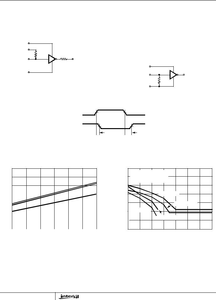
HIN232, HIN236, HIN237, HIN238, HIN239, HIN240, HIN241
impedance, VCC = 4.5V, and maximum allowable operating temperature. The transmitters have an internally limited output slew rate which is less than 30V/µs. The outputs are short circuit protected and can be shorted to ground indefinitely. The powered down output impedance is a minimum of 300Ω with
±2V applied to the outputs and VCC = 0V.
V+ |
|
|
|
VCC |
400kΩ |
|
|
|
300Ω |
|
|
TXIN |
|
|
|
|
T |
|
|
GND < TXIN < VCC |
|
OUT |
|
|
V- < V |
< V+ |
|
|
|
TOUT |
|
V- |
|
|
|
FIGURE 2. TRANSMITTER
Receivers
The receiver inputs accept up to ±30V while presenting the required 3kΩ to 7kΩ input impedance even if the power is off
(VCC = 0V). The receivers have a typical input threshold of 1.3V which is within the ±3V limits, known as the transition region, of the RS-232 specifications. The receiver output is 0V to VCC. The output will be low whenever the input is greater than 2.4V and high whenever the input is floating or driven between +0.8V and -30V. The receivers feature 0.5V hysteresis to improve noise rejection. The receiver Enable line EN, when set to logic “1”, (HIN236, 239, 240, and 241) disables the receiver outputs, placing them in the high impedance mode. The receiver outputs are also placed in the high impedance state when in shutdown mode.
VCC |
|
|
|
|
RXIN |
|
ROUT |
|
|
-30V < RXIN < +30V |
5kΩ |
GND < V |
ROUT |
< V |
|
|
|
CC |
|
GND |
|
|
|
|
FIGURE 3. RECEIVER
TIN
OR
RIN
TOUT
OR
ROUT
tPHL
VOL
VOL
tPLH 
Average Propagation Delay = tPHL + tPLH
2
FIGURE 4. PROPAGATION DELAY DEFINITION
Typical Performance Curves
V- SUPPLY VOLTAGE
12
1µF
10
|
|
|
|
|
|
0.47µF |
|
|
8 |
|
|
|
|
|
|
|
|
|
|
|
|
|
0.10µF |
|
|
|
6 |
|
|
|
|
|
|
|
|
|
|
|
|
|
|
|
|
|
|
|
|
|
|
|
|
|
|
4 |
|
|
|
|
|
|
|
|
|
|
|
|
|
|
|
|
|
2 |
|
|
|
|
|
|
|
|
|
|
|
|
|
|
|
|
|
0 |
|
|
|
|
|
|
|
|
|
3.5 |
4.0 |
4.5 |
5.0 |
5.5 |
6.0 |
||
3.0 |
||||||||
VCC
TA = 25oC
12TRANSMITTER OUTPUTS OPEN CIRCUIT
(|V|) |
10 |
|
|
|
|
|
|
|
|
|
|
|
|
|
|
|
|
VOLTAGE |
8 |
|
|
V+ (VCC = 5V) |
|
|
|
|
6 |
|
|
|
V+ (VCC = 4.5V) |
|
|
||
SUPPLY |
|
|
|
|
|
|||
4 |
V- (VCC = 4.5V) |
|
|
|
|
|
|
|
|
|
|
V- (VCC = 5V) |
|
|
|
||
|
2 |
|
|
|
|
|
||
|
|
|
|
|
|
|
|
|
|
0 |
5 |
10 |
15 |
20 |
25 |
30 |
35 |
|
0 |
|||||||
|
|
|
|
|ILOAD| (mA) |
|
|
|
|
FIGURE 5. V- SUPPLY VOLTAGE vs VCC , VARYING |
FIGURE 6. V+, V- OUTPUT VOLTAGE vs LOAD (HIN232) |
CAPACITORS |
|
9

HIN232, HIN236, HIN237, HIN238, HIN239, HIN240, HIN241
Test Circuits (HIN232)
1µF |
- |
|
C3 |
+ |
C1+ |
|
1 |
1µF |
|
+ |
|
|
V+ |
||
|
2 |
||||||
|
|
|
|
||||
C1 |
|
- |
|
|
C1- |
||
|
|
|
|||||
3 |
|||||||
|
|
|
|
|
|||
1µF |
+ |
4 |
C2+ |
C2 |
- |
5 |
C2- |
|
|
|
+ |
|
- |
|
V- |
|||
|
|
|
|
|
1µ |
|
C4 |
6 |
||
|
|
|
|
|
F |
|
T2OUT |
|||
3kΩ |
|
|
|
|
||||||
|
|
|
|
|
|
|
7 |
|||
 8 R2IN
T2 
OUTPUT
RS-232 
±30V INPUT
|
|
|
|
|
|
+4.5V TO |
||||||||
|
|
|
|
|
+5.5V INPUT |
|||||||||
|
|
|
|
|
||||||||||
|
|
|
|
|
|
|
|
|
|
|
|
|
|
|
|
|
|
|
|
|
|
|
|
|
|
|
|
|
|
|
|
|
|
|
|
|
|
|
|
|
|
|
|
|
|
VCC |
16 |
|
|
|
|
|
|
|
|
|
|
|
|
|
|
|
|
|
|
|
|
|
|
|
|
|
||
|
|
|
|
|
|
|
|
|
|
|
|
3kΩ |
||
|
|
|
|
|
|
|
|
|
|
|
|
|||
|
GND |
15 |
|
|||||||||||
|
|
|
|
|
|
|
|
|
|
|
|
|
||
T1OUT |
14 |
|
|
|
T1 OUTPUT |
|||||||||
|
R1IN |
|
|
RS-232 ±30V INPUT |
||||||||||
|
13 |
|
||||||||||||
R1OUT |
|
|
TTL/CMOS OUTPUT |
|||||||||||
12 |
|
|||||||||||||
|
T1IN |
|
|
TTL/CMOS INPUT |
||||||||||
|
11 |
|
||||||||||||
|
T2IN |
|
|
TTL/CMOS INPUT |
||||||||||
|
10 |
|
||||||||||||
R2OUT |
|
|
TTL/CMOS OUTPUT |
|||||||||||
9 |
|
|||||||||||||
|
|
|
|
|
|
|
|
|
|
|
|
|
|
|
|
|
|
|
|
|
|
|
|
|
|
|
C1+ |
|
VCC |
|
|
|
|
|
1 |
|
16 |
|
|
||
|
|
|
|
|
||||
|
|
|
V+ |
|
GND |
|
|
|
|
|
2 |
|
15 |
|
|
||
|
|
|
C1- |
T1OUT |
|
|
|
|
|
|
3 |
14 |
|
|
|||
|
|
|
C2+ |
|
R1IN |
|
|
|
|
|
4 |
|
13 |
|
|
||
|
|
|
C2- |
R1OUT |
|
|
|
|
|
|
5 |
12 |
|
|
|||
|
|
|
V- |
|
T1IN |
|
|
|
|
|
6 |
11 |
|
|
|||
|
|
|
|
|
||||
|
|
|
T2OUT |
|
T2IN |
|
|
|
|
|
7 |
|
10 |
|
|
||
|
|
|
R2IN |
R2OUT |
|
|
|
|
|
|
8 |
9 |
|
|
|||
|
|
|
|
|
|
|
|
|
|
|
|
|
|
|
|
|
|
ROUT = VIN/1T2OUT

|
T1OUT |
VIN = ±2V |
A |
FIGURE 7. GENERAL TEST CIRCUIT |
FIGURE 8. POWER-OFF SOURCE RESISTANCE |
|
CONFIGURATION |
Applications
The HIN2XX may be used for all RS-232 data terminal and communication links. It is particularly useful in applications where ±12V power supplies are not available for conventional RS-232 interface circuits. The applications presented represent typical interface configurations.
A simple duplex RS-232 port with CTS/RTS handshaking is illustrated in Figure 9. Fixed output signals such as DTR (data terminal ready) and DSRS (data signaling rate select) is generated by driving them through a 5kΩ resistor connected to V+.
In applications requiring four RS-232 inputs and outputs (Figure 10), note that each circuit requires two charge pump capacitors (C1 and C2) but can share common reservoir capacitors (C3 and C4). The benefit of sharing common reservoir capacitors is the elimination of two capacitors and the reduction of the charge pump source impedance which effectively increases the output swing of the transmitters.
+5V 
 -
-
+ |
|
|
1 |
|
16 |
|
|
DTR (20) DATA |
|
C1 + |
3 |
|
|
2 |
|
TERMINAL READY |
1µF - |
|
HIN232 |
|
|
DSRS (24) DATA |
||
|
|
4 |
|
6 |
|
SIGNALING RATE |
|
|
C2 + |
|
|
- |
SELECT |
||
|
|
|
|
|
RS-232 |
||
1µF - |
5 |
|
|
|
+ |
||
|
|
11 |
|
T1 |
14 |
|
INPUTS AND OUTPUTS |
|
TD |
|
|
TD (2) TRANSMIT DATA |
|||
|
|
T2 |
|
||||
|
|
10 |
|
7 |
|
RTS (4) REQUEST TO SEND |
|
TTL/CMOS |
RTS |
|
|
|
|||
INPUTS AND |
12 |
|
|
13 |
|
RD (3) RECEIVE DATA |
|
OUTPUTS |
RD |
9 |
R2 |
R1 |
8 |
|
|
|
CTS |
|
CTS (5) CLEAR TO SEND |
||||
|
|
|
|
|
|
||
|
|
|
|
15 |
|
|
SIGNAL GROUND (7) |
FIGURE 9. SIMPLE DUPLEX RS-232 PORT WITH CTS/RTS HANDSHAKING
10