

MOTOROLA
SEMICONDUCTOR TECHNICAL DATA
Order this document by BUL44D2/D
Designer's Data Sheet
High Speed, High Gain Bipolar NPN Power Transistor with Integrated Collector-Emitter Diode and Built-in Efficient Antisaturation Network
The BUL44D2 is state±of±art High Speed High gain BIPolar transistor (H2BIP). High dynamic characteristics and lot to lot minimum spread (±150 ns on storage time) make it ideally suitable for light ballast applications. Therefore, there is no need to guarantee an hFE window.
Main features:
•Low Base Drive Requirement
•High Peak DC Current Gain (55 Typical) @ IC = 100 mA
•Extremely Low Storage Time Min/Max Guarantees Due to the H2BIP Structure which Minimizes the Spread
•Integrated Collector±Emitter Free Wheeling Diode
•Fully Characterized and Guaranteed Dynamic VCE(sat)
•ª6 Sigmaº Process Providing Tight and Reproductible Parameter Spreads
It's characteristics make it also suitable for PFC application.
MAXIMUM RATINGS
BUL44D2
POWER TRANSISTORS
2 AMPERES
700 VOLTS
50 WATTS
CASE 221A±06
TO±220AB
Rating |
Symbol |
Value |
Unit |
|
|
|
|
Collector±Emitter Sustaining Voltage |
VCEO |
400 |
Vdc |
Collector±Base Breakdown Voltage |
VCBO |
700 |
Vdc |
Collector±Emitter Breakdown Voltage |
VCES |
700 |
Vdc |
Emitter±Base Voltage |
VEBO |
12 |
Vdc |
Collector Current Ð Continuous |
IC |
2 |
Adc |
Ð Peak (1) |
ICM |
5 |
|
Base Current Ð Continuous |
IB |
1 |
Adc |
Base Current Ð Peak (1) |
IBM |
2 |
|
*Total Device Dissipation @ TC = 25_C |
PD |
50 |
Watt |
*Derate above 25°C |
|
0.4 |
W/_C |
|
|
|
|
Operating and Storage Temperature |
TJ, Tstg |
± 65 to 150 |
_C |
THERMAL CHARACTERISTICS
Thermal Resistance |
|
|
_C/W |
Ð Junction to Case |
RqJC |
2.5 |
|
Ð Junction to Ambient |
RqJA |
62.5 |
|
Maximum Lead Temperature for Soldering Purposes: |
TL |
260 |
_C |
1/8″ from case for 5 seconds |
|
|
|
|
|
|
|
(1) Pulse Test: Pulse Width = 5 ms, Duty Cycle ≤ 10%. |
|
|
|
Designer's and SWITCHMODE are trademarks of Motorola, Inc.
Designer's Data for ªWorst Caseº Conditions Ð The Designer 's Data Sheet permits the design of most circuits entirely from the information presented. SOA Limit curves Ð representing boundaries on device characteristics Ð are given to facilitate ªworst caseº design.
Motorola, Inc. 1995

BUL44D2
ELECTRICAL CHARACTERISTICS (TC = 25°C unless otherwise noted)
Characteristic |
|
Symbol |
Min |
Typ |
Max |
Unit |
|
|
|
|
|
|
|
OFF CHARACTERISTICS |
|
|
|
|
|
|
|
|
|
|
|
|
|
Collector±Emitter Sustaining Voltage |
|
VCEO(sus) |
400 |
470 |
|
Vdc |
(IC = 100 mA, L = 25 mH) |
|
|
|
|
|
|
Collector±Base Breakdown Voltage |
|
VCBO |
700 |
920 |
|
Vdc |
(ICBO = 1 mA) |
|
|
|
|
|
|
Emitter±Base Breakdown Voltage |
|
VEBO |
12 |
14.5 |
|
Vdc |
(IEBO = 1 mA) |
|
|
|
|
|
|
Collector Cutoff Current |
@ TC = 25°C |
ICEO |
|
|
50 |
μAdc |
(VCE = Rated VCEO, IB = 0) |
@ TC = 125°C |
|
|
|
500 |
|
Collector Cutoff Current (VCE = Rated VCES, VEB = 0) |
@ TC = 25°C |
ICES |
|
|
50 |
μAdc |
|
@ TC = 125°C |
|
|
|
500 |
|
Collector Cutoff Current (VCE = 500 V, VEB = 0) |
@ TC = 125°C |
|
|
|
100 |
|
Emitter±Cutoff Current |
|
IEBO |
|
|
100 |
μAdc |
(VEB = 10 Vdc, IC = 0) |
|
|
|
|
|
|
ON CHARACTERISTICS |
|
|
|
|
|
|
|
|
|
|
|
|
|
Base±Emitter Saturation Voltage |
@ TC = 25°C |
VBE(sat) |
|
|
|
Vdc |
(IC = 0.4 Adc, IB = 40 mAdc) |
|
|
0.78 |
0.9 |
|
|
|
@ TC = 125°C |
|
|
0.65 |
0.8 |
|
(IC = 1 Adc, IB = 0.2 Adc) |
@ TC = 25°C |
|
|
0.87 |
1 |
|
|
@ TC = 125°C |
|
|
0.76 |
0.9 |
|
Collector±Emitter Saturation Voltage |
@ TC = 25°C |
VCE(sat) |
|
|
|
Vdc |
(IC = 0.4 Adc, IB = 40 mAdc) |
|
|
0.25 |
0.4 |
|
|
|
@ TC = 125°C |
|
|
0.27 |
0.5 |
|
(IC = 1 Adc, IB = 0.2 Adc) |
@ TC = 25°C |
|
|
0.28 |
0.5 |
|
|
@ TC = 125°C |
|
|
0.35 |
0.6 |
|
(IC = 0.4 Adc, IB = 20 mAdc) |
@ TC = 25°C |
|
|
0.45 |
0.65 |
|
|
@ TC = 125°C |
|
|
0.67 |
1 |
|
DC Current Gain |
@ TC = 25°C |
hFE |
|
|
|
Ð |
(IC = 0.4 Adc, VCE = 1 Vdc) |
|
20 |
32 |
|
|
|
|
@ TC = 125°C |
|
18 |
26 |
|
|
(IC = 1 Adc, VCE = 1 Vdc) |
@ TC = 25°C |
|
10 |
14 |
|
|
|
@ TC = 125°C |
|
7 |
9.5 |
|
|
DIODE CHARACTERISTICS |
|
|
|
|
|
|
|
|
|
|
|
|
|
Forward Diode Voltage |
@ TC = 25°C |
VEC |
|
1.1 |
1.5 |
V |
(IEC = 1 Adc) |
|
|
|
|
|
|
(IEC = 0.4 Adc) |
@ TC = 25°C |
|
|
0.9 |
1.2 |
|
(IEC = 0.2 Adc) |
@ TC = 25°C |
|
|
0.8 |
1 |
|
(IEC = 0.2 Adc) |
@ TC = 125°C |
|
|
0.6 |
|
|
Forward Recovery Time (see Figure 22 bis) |
|
Tfr |
|
415 |
|
ns |
(IF = 0.2 Adc, di/dt = 10 A/μs) |
@ TC = 25°C |
|
|
|
|
|
(IF = 0.4 Adc, di/dt = 10 A/μs) |
@ TC = 25°C |
|
|
390 |
|
|
(IF = 1 Adc, di/dt = 10 A/μs) |
@ TC = 25°C |
|
|
340 |
|
|
2 |
Motorola Bipolar Power Transistor Device Data |

|
|
|
|
|
|
|
|
|
|
|
|
|
|
|
|
BUL44D2 |
|
ELECTRICAL CHARACTERISTICS (TC = 25°C unless otherwise noted) |
|
|
|
|
|
|
|||||||||||
|
|
|
|
|
|
|
|
|
|
|
|
||||||
|
|
Characteristic |
|
|
Symbol |
Min |
Typ |
Max |
|
Unit |
|||||||
|
|
|
|
|
|
|
|
|
|
|
|
||||||
DYNAMIC SATURATION VOLTAGE |
|
|
|
|
|
|
|
|
|
|
|||||||
|
|
|
|
|
|
|
|
|
|
|
|
|
|
|
|
|
|
|
|
|
I |
|
|
= 0.4 A |
|
@ 1 μs |
@ TC = 25°C |
|
VCE(dsat) |
|
3.3 |
|
|
V |
|
|
|
|
|
|
|
|
° |
|
|
|
6.8 |
|
|
|
|||
|
|
|
C |
|
|
|
|
|
@ TC = 125 C |
|
|
|
|
|
|
||
Dynamic Saturation |
|
IB1 = 40 mA |
|
|
|
|
|
|
|
|
|
|
|||||
|
|
@ 3 μs |
@ TC = 25°C |
|
|
|
0.5 |
|
|
V |
|||||||
Voltage: |
|
VCC = 300 V |
|
|
|
|
|
|
|||||||||
μ |
|
|
|
|
|
|
|
|
|
@ TC = 125°C |
|
|
|
1.3 |
|
|
|
Determined 1 s and |
|
|
|
|
|
|
|
|
|
|
|
|
|
|
|
|
|
3 μs respectively after |
|
|
|
|
|
|
|
|
|
|
|
|
|
|
|
|
|
|
|
|
|
|
|
|
|
@ 1 μs |
@ TC = 25°C |
|
|
|
4.4 |
|
|
V |
|
rising IB1 reaches |
|
|
I |
|
|
|
= 1 A |
|
|
|
|
|
|
||||
|
|
C |
|
|
° |
|
|
|
12.8 |
|
|
|
|||||
90% of final IB1 |
|
I |
= 0.2 A |
|
|
@ TC = 125 C |
|
|
|
|
|
|
|||||
|
|
|
B1 |
|
|
|
@ 3 μs |
@ TC = 25°C |
|
|
|
0.5 |
|
|
V |
||
|
|
VCC = 300 V |
|
|
|
|
|
|
|||||||||
|
|
|
|
|
|
|
|
|
|
@ TC = 125°C |
|
|
|
1.8 |
|
|
|
DYNAMIC CHARACTERISTICS |
|
|
|
|
|
|
|
|
|
|
|
|
|
|
|||
|
|
|
|
|
|
|
|
|
|
|
|
|
|
|
|
|
|
Current Gain Bandwidth |
|
|
|
|
|
|
|
|
|
|
fT |
|
13 |
|
|
MHz |
|
(IC = 0.5 Adc, VCE = 10 Vdc, f = 1 MHz) |
|
|
|
|
|
|
|
|
|
|
|||||||
Output Capacitance |
|
|
|
|
|
|
|
|
|
|
Cob |
|
50 |
75 |
|
pF |
|
(VCB = 10 Vdc, IE = 0, f = 1 MHz) |
|
|
|
|
|
|
|
|
|
|
|||||||
Input Capacitance |
|
|
|
|
|
|
|
|
|
|
Cib |
|
240 |
500 |
|
pF |
|
(VEB = 8 Vdc) |
|
|
|
|
|
|
|
|
|
|
|
|
|
|
|
|
|
SWITCHING CHARACTERISTICS: Resistive Load (D.C. ≤ 10%, Pulse Width = 40 μs) |
|
|
|
|
|
||||||||||||
|
|
|
|
|
|
|
|
|
|
|
|
|
|
|
|
||
Turn±on Time |
I |
= 0.5 Adc, I |
= 50 mAdc |
@ TC = 25°C |
|
ton |
|
450 |
600 |
|
ns |
||||||
|
° |
|
|
|
600 |
|
|
|
|||||||||
|
C |
|
|
|
|
|
B1 |
|
|
@ TC = 125 C |
|
|
|
|
|
|
|
|
|
|
|
IB2 = 250 mAdc |
|
|
|
|
|
|
|
|
|||||
Turn±off Time |
|
|
|
@ TC = 25°C |
|
toff |
700 |
|
1000 |
|
ns |
||||||
|
|
|
|
V = 300 Vdc |
|
|
|
||||||||||
|
|
|
|
|
|
|
CC |
|
|
@ TC = 125°C |
|
|
|
1300 |
|
|
|
|
|
|
|
|
|
|
|
|
|
|
|
|
|
|
|
||
Turn±on Time |
I |
|
= 1 Adc, I |
= 0.2 Adc |
@ TC = 25°C |
|
ton |
|
90 |
150 |
|
ns |
|||||
|
|
° |
|
|
|
105 |
|
|
|
||||||||
|
C |
|
|
|
|
B1 |
|
|
@ TC = 125 C |
|
|
|
|
|
|
||
|
|
|
|
|
|
|
IB2 = 0.5 Adc |
|
|
|
|
|
|
|
|
||
Turn±off Time |
|
|
|
|
|
|
@ TC = 25°C |
|
toff |
|
1.1 |
1.25 |
|
μs |
|||
|
|
|
|
VCC = 300 Vdc |
|
|
|
||||||||||
|
|
|
|
|
|
|
|
|
|
@ TC = 125°C |
|
|
|
1.5 |
|
|
|
SWITCHING CHARACTERISTICS: Inductive Load (Vclamp = 300 V, VCC = 15 V, L = 200 μH) |
|
|
|
|
|||||||||||||
Fall Time |
|
|
|
|
|
|
|
|
|
@ TC = 25°C |
|
tf |
|
110 |
150 |
|
ns |
|
|
|
|
|
|
|
IC = 0.4 Adc |
@ TC = 125°C |
|
|
|
105 |
|
|
|
||
Storage Time |
|
|
|
|
|
|
@ TC = 25°C |
|
ts |
|
0.55 |
0.75 |
|
μs |
|||
|
|
|
|
IB1 = 40 mAdc |
|
|
|
||||||||||
|
|
|
|
|
@ TC = 125°C |
|
|
|
0.70 |
|
|
|
|||||
|
|
|
|
|
|
|
IB2 = 0.2 Adc |
|
|
|
|
|
|
||||
Crossover Time |
|
|
|
|
|
|
|
|
|
@ TC = 25°C |
|
tc |
|
85 |
150 |
|
ns |
|
|
|
|
|
|
|
|
|
|
@ TC = 125°C |
|
|
|
80 |
|
|
|
Fall Time |
|
|
|
|
|
|
|
|
|
@ TC = 25°C |
|
tf |
|
100 |
150 |
|
ns |
|
|
|
|
|
|
|
IC = 1 Adc |
@ TC = 125°C |
|
|
|
90 |
|
|
|
||
Storage Time |
|
|
|
|
|
|
@ TC = 25°C |
|
ts |
|
1.05 |
1.5 |
|
μs |
|||
|
|
|
|
|
|
IB1 = 0.2 Adc |
|
|
|
||||||||
|
|
|
|
|
|
|
@ TC = 125°C |
|
|
|
1.45 |
|
|
|
|||
|
|
|
|
|
|
|
IB2 = 0.5 Adc |
|
|
|
|
|
|
||||
Crossover Time |
|
|
|
|
|
|
|
|
|
@ TC = 25°C |
|
tc |
|
100 |
175 |
|
ns |
|
|
|
|
|
|
|
|
|
|
@ TC = 125°C |
|
|
|
100 |
|
|
|
Fall Time |
|
|
|
|
|
|
|
|
|
@ TC = 25°C |
|
tf |
|
110 |
150 |
|
ns |
|
|
|
|
|
|
|
IC = 0.8 Adc |
@ TC = 125°C |
|
|
|
180 |
|
|
|
||
Storage Time |
|
|
|
|
|
|
@ TC = 25°C |
|
ts |
2.05 |
|
2.35 |
|
μs |
|||
|
|
|
IB1 = 160 mAdc |
|
|
|
|||||||||||
|
|
|
|
@ TC = 125°C |
|
|
|
2.8 |
|
|
|
||||||
|
|
|
|
IB2 = 160 mAdc |
|
|
|
|
|
|
|||||||
Crossover Time |
|
|
|
|
|
|
|
|
|
@ TC = 25°C |
|
tc |
|
180 |
300 |
|
ns |
|
|
|
|
|
|
|
|
|
|
@ TC = 125°C |
|
|
|
400 |
|
|
|
Fall Time |
|
|
|
|
|
|
|
|
|
@ TC = 25°C |
|
tf |
|
150 |
225 |
|
ns |
|
|
|
|
|
|
|
IC = 0.4 Adc |
@ TC = 125°C |
|
|
|
175 |
|
|
|
||
Storage Time |
|
|
|
|
|
|
@ TC = 25°C |
|
ts |
1.65 |
|
1.95 |
|
μs |
|||
|
|
|
|
IB1 = 40 mAdc |
|
|
|
||||||||||
|
|
|
|
|
@ TC = 125°C |
|
|
|
2.2 |
|
|
|
|||||
|
|
|
|
|
IB2 = 40 mAdc |
|
|
|
|
|
|
||||||
Crossover Time |
|
|
|
|
|
|
|
|
|
@ TC = 25°C |
|
tc |
|
150 |
250 |
|
ns |
|
|
|
|
|
|
|
|
|
|
@ TC = 125°C |
|
|
|
330 |
|
|
|
Motorola Bipolar Power Transistor Device Data |
3 |

BUL44D2
TYPICAL STATIC CHARACTERISTICS
|
100 |
|
|
|
|
|
VCE = 1 V |
|
|
|
|
GAIN |
80 |
|
|
|
|
|
TJ = 125°C |
|
|
|
|
CURRENT |
60 |
TJ = 25°C |
|
|
|
40 |
|
|
|
|
|
DC |
TJ = ± 20°C |
|
|
|
|
|
|
|
|
||
, |
|
|
|
|
|
FE |
|
|
|
|
|
h |
20 |
|
|
|
|
|
|
|
|
|
|
|
0 |
|
|
|
|
|
0.001 |
0.01 |
0.1 |
1 |
10 |
|
|
IC, COLLECTOR CURRENT (AMPS) |
|
||
Figure 1. DC Current Gain @ 1 Volt
|
4 |
|
|
|
|
|
|
|
TJ = 25°C |
(VOLTS) |
3 |
|
|
|
|
|
|
2 A |
|
, VOLTAGE |
2 |
|
|
|
|
|
|
||
|
|
1.5 A |
|
|
|
|
|
|
|
CE |
|
|
1 A |
|
V |
1 |
|
|
|
|
|
|
|
|
|
|
|
400 mA |
|
|
0 |
IC = 200 mA |
|
|
|
|
|
|
|
|
1 |
10 |
100 |
1000 |
|
|
IB, BASE CURRENT (mA) |
|
|
Figure 3. Collector Saturation Region
|
10 |
|
|
|
|
|
|
IC/IB = 10 |
|
|
|
(VOLTS) |
|
|
|
|
|
,VOLTAGE |
1 |
|
|
|
|
|
|
|
TJ = 25°C |
|
|
CE |
|
|
TJ = 125°C |
|
|
V |
|
|
|
|
|
|
|
|
|
TJ = ± 20°C |
|
|
0.1 |
|
|
1 |
|
|
0.001 |
0.01 |
0.1 |
10 |
|
|
|
IC, COLLECTOR CURRENT (AMPS) |
|
||
Figure 5. Collector±Emitter Saturation Voltage
|
100 |
|
|
|
|
|
VCE = 5 V |
|
|
|
|
GAIN |
80 |
TJ = 125°C |
|
|
|
|
|
|
|
||
|
|
|
|
|
|
DC CURRENT |
60 |
TJ = 25°C |
|
|
|
40 |
TJ = ± 20°C |
|
|
|
|
, |
|
|
|
|
|
FE |
|
|
|
|
|
h |
20 |
|
|
|
|
|
|
|
|
|
|
|
0 |
|
|
|
|
|
0.001 |
0.01 |
0.1 |
1 |
10 |
|
|
IC, COLLECTOR CURRENT (AMPS) |
|
||
Figure 2. DC Current Gain @ 5 Volt
|
10 |
|
|
|
|
|
|
IC/IB = 5 |
|
|
|
(VOLTS) |
|
|
|
|
|
, VOLTAGE |
1 |
|
|
|
|
|
|
|
TJ = 125°C |
|
|
CE |
|
|
|
|
|
V |
|
|
TJ = 25°C |
|
|
|
|
|
|
|
|
|
0.1 |
|
|
TJ = ± 20°C |
|
|
|
|
|
|
|
|
0.001 |
0.01 |
0.1 |
1 |
10 |
|
|
IC, COLLECTOR CURRENT (AMPS) |
|
||
Figure 4. Collector±Emitter Saturation Voltage
|
10 |
|
|
|
|
|
IC/IB = 20 |
|
|
(VOLTS) |
|
|
TJ = 25°C |
|
, VOLTAGE |
1 |
|
|
|
|
|
|
||
|
|
|
|
|
CE |
|
|
TJ = 125°C |
|
V |
|
|
|
|
|
|
|
TJ = ± 20°C |
|
|
0.1 |
|
|
|
|
0.001 |
0.01 |
0.1 |
1 |
|
|
IC, COLLECTOR CURRENT (AMPS) |
|
|
Figure 6. Collector±Emitter Saturation Voltage
4 |
Motorola Bipolar Power Transistor Device Data |

BUL44D2
TYPICAL STATIC CHARACTERISTICS
|
10 |
|
|
|
|
|
|
IC/IB = 5 |
|
|
|
(VOLTS) |
|
|
|
|
|
, VOLTAGE |
1 |
|
TJ = ± 20°C |
|
|
|
|
|
TJ = 125°C |
|
|
BE |
|
|
|
|
|
|
|
|
|
|
|
V |
|
|
TJ = 25°C |
|
|
|
|
|
|
|
|
|
0.1 |
|
|
|
|
|
0.001 |
0.01 |
0.1 |
1 |
10 |
IC, COLLECTOR CURRENT (AMPS)
Figure 7A. Base±Emitter Saturation Region
|
10 |
|
|
|
|
|
IC/IB = 20 |
|
|
(VOLTS) |
|
|
|
|
, VOLTAGE |
1 |
|
TJ = ± 20°C |
|
|
|
TJ = 125°C |
|
|
BE |
|
|
|
|
|
|
|
|
|
V |
|
|
TJ = 25°C |
|
|
|
|
|
|
|
0.1 |
|
|
|
|
0.001 |
0.01 |
0.1 |
1 |
|
|
IC, COLLECTOR CURRENT (AMPS) |
|
|
Figure 7C. Base±Emitter Saturation Region
|
10 |
|
|
|
|
|
|
IC/IB = 10 |
|
|
|
(VOLTS) |
|
|
|
|
|
, VOLTAGE |
1 |
|
TJ = ± 20°C |
|
|
|
|
|
TJ = 125°C |
|
|
BE |
|
|
|
|
|
|
|
|
|
|
|
V |
|
|
TJ = 25°C |
|
|
|
|
|
|
|
|
|
0.1 |
|
|
|
|
|
0.001 |
0.01 |
0.1 |
1 |
10 |
IC, COLLECTOR CURRENT (AMPS)
Figure 7B. Base±Emitter Saturation Region
|
10 |
|
|
|
(VOLTS) |
|
|
|
|
VOLTAGE |
|
|
25°C |
|
1 |
|
|
|
|
FORWARD DIODE |
|
|
|
|
|
|
|
125°C |
|
|
|
|
|
|
|
0.1 |
|
1 |
|
|
0.01 |
0.1 |
10 |
REVERSE EMITTER±COLLECTOR CURRENT (AMPS)
Figure 8. Forward Diode Voltage
Motorola Bipolar Power Transistor Device Data |
5 |
BUL44D2
TYPICAL SWITCHING CHARACTERISTICS
|
1000 |
|
|
1000 |
|
|
Cib (pF) |
TJ = 25°C |
|
|
|
f(test) = 1 MHz |
800 |
|
|
|
|
|
|
(pF) |
100 |
|
|
|
CAPACITANCE |
|
|
Cob (pF) |
600 |
|
|
|
||
|
|
t,TIME(ns) |
400 |
|
10 |
|
|
||
C, |
|
|
|
|
|
|
|
|
|
|
|
|
|
200 |
|
1 |
|
|
0 |
|
1 |
10 |
100 |
|
|
IBon = IBoff |
TJ = 125°C |
|
|
VCC = 300 V |
TJ = 25°C |
|
|
PW = 40 μs |
|
|
|
|
IC/IB = 10 |
|
|
IC/IB = 5 |
|
|
0.2 |
0.8 |
1.4 |
2 |
VR, REVERSE VOLTAGE (VOLTS) |
IC, COLLECTOR CURRENT (AMPS) |
Figure 9. Capacitance |
Figure 10. Resistive Switch Time, ton |
|
4000 |
|
|
|
|
|
|
|
IC/IB = 10 |
IBon = IBoff |
|
|
3500 |
|
V |
= 300 V |
|
|
|
|
|
CC |
|
|
|
|
|
PW = 40 μs |
|
μs) |
3000 |
|
|
|
|
|
|
|
|
|
|
( |
|
|
|
|
|
t, TIME |
2500 |
|
|
|
|
2000 |
|
|
|
|
|
|
|
|
|
|
|
|
1500 |
TJ = 125°C |
|
|
|
|
|
TJ = 25°C |
IC/IB = 5 |
|
|
|
1000 |
|
|
|
|
|
0 |
1 |
|
|
2 |
|
3 |
|
|
|
|
|
|
2.5 |
|
|
|
|
|
μs) |
2 |
|
|
|
|
|
|
|
|
|
|
|
|
( |
|
|
|
|
|
|
t, TIME |
1.5 |
|
|
|
|
|
1 |
|
|
|
|
|
|
|
|
|
IBon = IBoff |
|||
|
|
|
|
|||
|
0.5 |
TJ = 125°C |
|
VCC = 15 V |
||
|
|
V |
= 300 V |
|||
|
|
TJ = 25°C |
|
Z |
|
μH |
|
|
|
L |
= 200 |
||
|
|
|
|
C |
|
|
|
0 |
|
1.2 |
|
|
|
|
0.4 |
0.8 |
1.6 |
2 |
||
IC, COLLECTOR CURRENT (AMPS) |
IC, COLLECTOR CURRENT (AMPS) |
Figure 11. Resistive Switch Time, toff
|
700 |
|
|
TJ = 125°C |
|
|
|
|
|
|
|
IC/IBon = 5 |
|
|
|
|
600 |
|
|
TJ = 25°C |
|
|
|
|
500 |
IBon = IBoff |
|
|
tc |
||
(ns) |
|
V |
CC |
= 15 V |
|
|
|
400 |
VZ = 300 V |
|
|
|
|||
TIME |
|
LC = 200 μH |
|
|
|
||
300 |
|
|
|
|
|
|
|
t, |
|
|
|
|
|
|
|
|
|
|
|
|
|
|
|
|
200 |
|
|
|
|
|
tfi |
|
|
|
|
|
|
|
|
|
100 |
|
|
|
|
|
|
|
0 |
|
|
|
|
|
|
|
0 |
|
|
0.5 |
1 |
1.5 |
2 |
IC, COLLECTOR CURRENT (AMPS)
Figure 13. Inductive Switching,
tc & tfi @ IC/IB = 5
Figure 12. Inductive Storage Time,
|
|
tsi @ IC/IB = 5 |
|
|
|
|
|
4 |
|
|
|
|
|
|
|
TJ = 125°C |
|
|
|
|
|
|
TJ = 25°C |
|
|
|
|
s) |
3 |
|
|
|
|
|
(μ |
|
IC = 1 A |
|
|
|
|
TIME |
|
|
|
|
|
|
|
|
|
|
|
|
|
,STORAGE |
2 |
|
|
|
|
|
|
|
|
I |
= I |
Boff |
|
si |
|
|
|
|||
t |
1 |
|
|
Bon |
|
|
|
IC = 0.3 A |
|
VCC = 15 V |
|||
|
|
|
||||
|
|
|
|
VZ = 300 V |
||
|
0 |
|
|
LC = 200 μH |
||
|
|
9 |
|
|
|
|
|
3 |
6 |
12 |
|
15 |
|
hFE, FORCED GAIN
Figure 14. Inductive Storage Time
6 |
Motorola Bipolar Power Transistor Device Data |

BUL44D2
TYPICAL SWITCHING CHARACTERISTICS
|
700 |
|
|
|
|
|
|
|
|
600 |
IBoff = IBon |
|
TJ = 125°C |
|
|
|
|
|
VCC = 15 V |
|
TJ = 25°C |
|
|
|
||
|
500 |
VZ = 300 V |
|
|
|
|
|
|
|
μ |
H |
|
|
|
|
|
|
(ns) |
|
LC = 200 |
|
|
IC = 0.3 A |
|
|
|
TIME |
400 |
|
|
|
|
|
|
|
|
|
|
|
|
|
|
|
|
, FALL |
300 |
|
|
|
|
|
|
|
|
|
|
|
|
|
|
|
|
fi |
|
|
|
|
|
|
|
|
t |
200 |
|
|
|
|
|
|
|
|
|
|
|
|
|
|
|
|
|
100 |
|
|
|
IC = 1 A |
|
|
|
|
0 |
|
|
|
|
|
|
|
|
|
|
|
|
|
|
|
|
|
3 |
5 |
|
7 |
9 |
11 |
13 |
15 |
|
|
|
|
|
hFE, FORCED GAIN |
|
|
|
Figure 15. Inductive Fall Time
|
900 |
TJ = 125°C |
|
|
|
|
800 |
|
|
|
|
|
TJ = 25°C |
|
|
|
|
|
|
|
|
|
|
|
700 |
|
|
|
|
|
600 |
|
IC/IB = 20 |
|
|
(ns) |
500 |
|
|
|
|
TIME |
400 |
|
|
|
|
t, |
300 |
|
|
|
|
|
|
|
IC/IB = 10 |
||
|
|
|
|
||
|
200 |
|
|
|
|
|
100 |
|
|
IBon = IBoff |
VZ = 300 V |
|
0 |
|
|
VCC = 15 V |
LC = 200 μH |
|
0.4 |
0.8 |
1.2 |
1.6 |
2 |
IC, COLLECTOR CURRENT (AMPS)
Figure 17. Inductive Switching, tfi
3000 |
|
|
|
|
|
|
|
IC/IB = 5 |
|
|
|
IBon = IBoff |
|
|
|
|
|
|
VCC = 15 V |
|
|
|
|
|
|
VZ = 300 V |
|
2000 |
|
|
|
|
LC = 200 μH |
|
|
|
|
|
|
|
|
TIME (ns) |
IB = 50 mA |
|
|
|
|
|
t, |
|
IB = 100 mA |
|
|
|
|
1000 |
|
|
|
|
||
|
|
|
IB = 200 mA |
|
|
|
|
|
|
|
IB = 500 mA |
|
|
0 |
|
|
|
|
|
|
0 |
0.5 |
1 |
1.5 |
2 |
2.5 |
3 |
IC, COLLECTOR CURRENT (AMPS)
Figure 19. Inductive Storage Time, tsi
|
1000 |
|
TJ = 125°C |
|
|
|
|
IBon = IBoff |
|
|
|
|
800 |
VCC = 15 V |
TJ = 25°C |
|
|
(ns) |
VZ = 300 V |
|
|
|
|
|
LC = 200 μH |
|
|
|
|
TIME |
|
|
|
|
|
600 |
|
|
IC = 1 A |
|
|
, CROSSOVER |
400 |
|
|
|
|
|
|
|
|
|
|
c |
|
|
|
|
|
t |
200 |
|
|
|
|
|
|
|
|
|
|
|
|
|
|
IC = 0.3 A |
|
|
0 |
|
|
|
|
|
3 |
6 |
9 |
12 |
15 |
hFE, FORCED GAIN
Figure 16. Inductive Crossover Time
|
2000 |
|
|
|
|
|
|
IBoff = IC/2 |
|
|
TJ = 125°C |
|
|
VCC = 15 V |
|
|
TJ = 25°C |
|
1500 |
VZ = 300 V |
|
|
|
|
|
LC = 200 μH |
|
IC/IB = 20 |
|
(ns) |
|
|
|
|
|
t, TIME |
1000 |
|
|
|
|
|
|
|
|
|
|
|
500 |
|
|
|
|
|
|
|
|
IC/IB = 10 |
|
|
0 |
|
1.2 |
|
|
|
0.4 |
0.8 |
1.6 |
2 |
|
|
|
IC, COLLECTOR CURRENT (AMPS) |
|
||
Figure 18. Inductive Switching, tc
|
3000 |
|
|
|
|
|
|
2500 |
|
|
|
IC/IB = 10 |
|
|
|
|
|
|
|
|
(ns) |
2000 |
|
|
|
|
|
|
|
|
IC/IB = 20 |
|
|
|
t, TIME |
|
|
|
|
|
|
1500 |
|
|
|
|
|
|
|
|
IBon = IBoff |
|
|
|
|
|
1000 |
VCC = 15 V |
|
TJ = 125°C |
|
|
|
|
V |
= 300 V |
|
|
|
|
|
Z |
= 200 μH |
|
TJ = 25°C |
|
|
|
L |
|
|
||
|
500 |
C |
|
|
|
|
|
0 |
0.5 |
1 |
1.5 |
2 |
|
|
|
|||||
IC, COLLECTOR CURRENT (AMPS)
Figure 20. Inductive Storage Time, tsi
Motorola Bipolar Power Transistor Device Data |
7 |

BUL44D2
TYPICAL SWITCHING CHARACTERISTICS
VCE |
dyn 1 μs |
|
|
||
|
|
dyn 3 μs |
0 V |
|
|
90% IB |
|
|
1 |
μs |
|
IB |
3 |
μs |
|
||
|
|
TIME |
Figure 21. Dynamic Saturation
Voltage Measurements
10 |
|
|
|
|
|
|
|
|
9 |
IC |
|
|
|
|
90% IC |
|
|
8 |
|
|
tsi |
|
|
tfi |
|
|
7 |
|
|
|
|
|
|
|
|
|
|
|
|
|
|
|
|
|
6 |
|
|
|
|
|
|
10% IC |
|
5 |
Vclamp |
|
10% Vclamp |
|
|
tc |
|
|
4 |
|
|
|
|
|
|
|
|
|
|
|
|
|
|
|
|
|
3 |
IB |
90% IB1 |
|
|
|
|
|
|
2 |
|
|
|
|
|
|
|
|
1 |
|
|
|
|
|
|
|
|
0 |
|
|
|
|
|
|
|
|
0 |
1 |
2 |
3 |
4 |
5 |
6 |
7 |
8 |
|
|
|
|
TIME |
|
|
|
|
Figure 22. Inductive Switching Measurements
|
|
VFRM |
VFR (1.1 VF unless |
|
|
|
|
|
otherwise specified) |
|
|
VF |
|
tfr |
|
VF |
|
|
|
|
|
|
|
|
0.1 VF |
|
|
|
|
0 |
|
|
|
|
|
IF |
|
|
|
|
|
|
10% IF |
|
|
|
|
0 |
2 |
4 |
6 |
8 |
10 |
Figure 22 bis. tfr Measurements
Table 1. Inductive Load Switching Drive Circuit
+15 V |
|
|
|
|
|
1 μF |
150 Ω |
100 Ω |
MTP8P10 |
100 μF |
|
|
|
||||
|
3 W |
3 W |
|
|
|
|
|
|
|
|
|
MPF930 |
|
|
MTP8P10 |
RB1 |
VCE |
|
|
MUR105 |
IB1 |
||
|
MPF930 |
|
|
||
+10 V |
|
|
Iout |
I |
|
|
|
|
|
|
B |
|
|
|
|
A |
|
50 Ω |
|
|
MJE210 |
RB2 |
|
|
|
|
|
||
|
|
|
|
|
|
COMMON |
|
150 Ω |
MTP12N10 |
|
|
|
|
|
V(BR)CEO(sus) |
||
|
500 μF |
3 W |
|
|
|
|
|
|
|
L = 10 mH |
|
|
|
|
|
1 μF |
RB2 = ∞ |
|
|
|
|
VCC = 20 Volts |
|
±Voff |
|
|
|
|
IC(pk) = 100 mA |
|
|
|
|
|
|
 IC PEAK
VCE PEAK 
IB2
Inductive Switching
L = 200 μH
RB2 = 0
VCC = 15 Volts RB1 selected for desired IB1
RBSOA
L = 500 μH
RB2 = 0
VCC = 15 Volts RB1 selected for desired IB1
8 |
Motorola Bipolar Power Transistor Device Data |

BUL44D2
TYPICAL CHARACTERISTICS
|
10 |
|
|
|
|
(AMPS) |
|
|
|
1 μs |
|
|
|
10 μs |
|
||
|
|
1 ms |
|
||
COLLECTOR CURRENT |
1 |
5 ms |
EXTENDED SOA |
||
|
|||||
|
DC |
|
|||
0.1 |
|
|
|||
|
|
|
|||
, |
|
|
|
|
|
C |
|
|
|
|
|
I |
|
|
|
|
|
|
0.01 |
|
|
|
|
|
10 |
100 |
|
1000 |
|
|
|
VCE, COLLECTOR±EMITTER VOLTAGE (VOLTS) |
|
||
Figure 23. Forward Bias Safe Operating Area
|
2.5 |
|
|
|
|
|
|
|
(AMPS) |
|
|
|
|
|
|
TC ≤ 125°C |
|
2 |
|
|
|
|
|
GAIN ≥ 4 |
|
|
|
|
|
|
|
LC = 500 μH |
|
||
|
|
|
|
|
|
|
||
CURRENT |
1.5 |
|
|
|
|
|
|
|
|
|
|
|
|
|
|
|
|
, COLLECTOR |
1 |
|
|
|
|
|
|
|
0.5 |
|
|
|
|
± 5 V |
|
|
|
C |
|
|
|
|
|
|
|
|
I |
|
|
0 V |
|
|
|
|
|
|
|
|
±1.5 V |
|
|
|
||
|
|
|
|
|
|
|
||
|
0 |
|
|
500 |
|
|
800 |
|
|
200 |
300 |
400 |
600 |
700 |
900 |
||
|
|
VCE, COLLECTOR±EMITTER VOLTAGE (VOLTS) |
|
|||||
Figure 24. Reverse Bias Safe Operating Area
|
1 |
|
|
|
|
|
|
|
|
|
|
|
|
SECOND BREAKDOWN |
|
||
FACTOR |
0.8 |
|
|
|
|
DERATING |
|
|
|
|
|
|
|
|
|
|
|
DERATING |
0.6 |
THERMAL DERATING |
|
|
|
|
||
|
|
|
|
|
||||
0.4 |
|
|
|
|
|
|
|
|
POWER |
|
|
|
|
|
|
|
|
0.2 |
|
|
|
|
|
|
|
|
|
|
|
|
|
|
|
|
|
|
0 |
40 |
60 |
80 |
|
120 |
140 |
|
|
20 |
100 |
160 |
|||||
|
|
|
TC, CASE TEMPERATURE (°C) |
|
|
|||
Figure 25. Forward Bias Power Derating
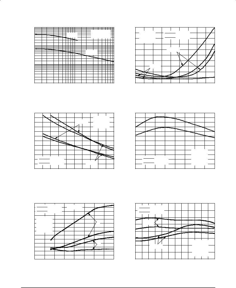
There are two limitations on the power handling ability of a transistor: average junction temperature and second breakdown. Safe operating area curves indicate IC ±VCE limits of the transistor that must be observed for reliable operation; i.e., the transistor must not be subjected to greater dissipation than the curves indicate. The data of Figure 23 is based
on TC = 25°C; TJ(pk) is variable depending on power level. Second breakdown pulse limits are valid for duty cycles to
10% but must be derated when TC > 25°C. Second breakdown limitations do not derate the same as thermal limitations. Allowable current at the voltages shown on Figure 23 may be found at any case temperature by using the appropriate curve on Figure 25.
TJ(pk) may be calculated from the data in Figure 26. At any case temperatures, thermal limitations will reduce the power
that can be handled to values less than the limitations imposed by second breakdown. For inductive loads, high voltage and current must be sustained simultaneously during turn±off with the base to emitter junction reverse biased. The safe level is specified as a reverse biased safe operating area (Figure 24). This rating is verified under clamped conditions so that the device is never subjected to an avalanche mode.
Motorola Bipolar Power Transistor Device Data |
9 |

BUL44D2
TYPICAL THERMAL RESPONSE
|
|
1 |
|
|
|
|
|
TRANSIENTTHERMAL RESISTANCE |
|
|
0.5 |
|
|
|
|
|
|
0.2 |
|
|
|
|
|
(NORMALIZED) |
|
0.1 |
|
|
|
|
|
0.1 |
0.05 |
|
P(pk) |
RθJC(t) = r(t) RθJC |
|
||
|
|
|
|
RθJC = 2.5°C/W MAX |
|
||
|
0.02 |
|
|
D CURVES APPLY FOR POWER |
|
||
|
|
|
t1 |
PULSE TRAIN SHOWN |
|
||
|
SINGLE PULSE |
|
READ TIME AT t1 |
|
|||
|
|
t |
|
||||
r(t), |
|
|
|
|
2 |
TJ(pk) ± TC = P(pk) RθJC(t) |
|
|
|
|
|
DUTY CYCLE, D = t1/t2 |
|
||
|
|
0.01 |
|
|
|
|
|
|
|
0.01 |
0.1 |
1 |
10 |
100 |
1000 |
t, TIME (ms)
Figure 26. Typical Thermal Response (ZθJC(t)) for BUL44D2
TYPICAL STATIC CHARACTERISTICS
|
1100 |
|
|
|
1000 |
TJ = 25°C |
|
(VOLTS) |
900 |
BVCER (VOLTS) @ 10 mA |
|
|
|
||
800 |
|
|
|
|
|
|
|
BVCER |
700 |
|
|
|
|
|
|
|
600 |
|
|
|
500 |
BVCER(sus) @ 200 mA |
|
|
|
|
|
|
400 |
|
|
|
10 |
100 |
1000 |
|
|
RBE (Ω) |
|
Figure 27. BVCER
|
440 |
|
|
|
|
(ns) |
420 |
|
|
dI/dt = 10 A/μs |
|
TIME |
|
|
|
||
400 |
|
|
TC = 25°C |
|
|
RECOVERY |
|
|
|
|
|
380 |
|
|
|
|
|
360 |
|
|
|
|
|
, FORWARD |
|
|
|
|
|
340 |
|
|
|
|
|
|
|
|
|
|
|
fr |
320 |
|
|
|
|
t |
|
|
|
|
|
|
|
|
|
|
|
|
300 |
|
|
1.5 |
|
|
0 |
0.5 |
1 |
2 |
IF, FORWARD CURRENT (AMP)
Figure 28. Forward Recovery Time tfr
10 |
Motorola Bipolar Power Transistor Device Data |