

MOTOROLA
SEMICONDUCTOR TECHNICAL DATA
High Voltage Power Transistors
DPAK For Surface Mount Applications
Designed for line operated audio output amplifier, switchmode power supply drivers and other switching applications.
•Lead Formed for Surface Mount Applications in Plastic Sleeves (No Suffix)
•Straight Lead Version in Plastic Sleeves (ª±1º Suffix)
•Lead Formed Version in 16 mm Tape and Reel (ªT4º Suffix)
•Electrically Similar to Popular TIP47, and TIP50
•250 and 400 V (Min) Ð V CEO(sus)
•1 A Rated Collector Current
MAXIMUM RATINGS
Rating |
Symbol |
MJD47 |
|
MJD50 |
Unit |
|
|
|
|
|
|
Collector±Emitter Voltage |
VCEO |
250 |
|
400 |
Vdc |
Collector±Base Voltage |
VCB |
350 |
|
500 |
Vdc |
Emitter±Base Voltage |
VEB |
|
5 |
Vdc |
|
Collector Current Ð Continuous |
IC |
|
1 |
Adc |
|
Peak |
|
|
2 |
|
|
|
|
|
|
|
|
Base Current |
IB |
|
0.6 |
Adc |
|
Total Power Dissipation @ TC = 25_C |
PD |
|
15 |
Watts |
|
Derate above 25_C |
|
|
0.12 |
W/_C |
|
|
|
|
|
|
|
Total Power Dissipation* @ TA = 25_C |
PD |
|
1.56 |
Watts |
|
Derate above 25_C |
|
0.0125 |
W/_C |
||
|
|
|
|
||
Operating and Storage Junction |
TJ, Tstg |
± 65 to +150 |
_C |
||
Temperature Range |
|
|
|
|
|
|
|
|
|
|
|
THERMAL CHARACTERISTICS
Characteristic |
|
Symbol |
|
Max |
|
|
|
Unit |
|
|
|
|
|
|
|
|
|
|
|
|
|
Thermal Resistance, Junction to Case |
|
RθJC |
|
8.33 |
|
|
|
_C/W |
|
|
Thermal Resistance, Junction to Ambient* |
RθJA |
|
80 |
|
|
|
_C/W |
|
||
Lead Temperature for Soldering Purpose |
|
TL |
|
260 |
|
|
|
_C |
|
|
ELECTRICAL CHARACTERISTICS (TC = 25_C unless otherwise noted) |
|
|
|
|
||||||
|
|
|
|
|
|
|
|
|
||
Characteristic |
|
|
Symbol |
Min |
Max |
|
|
Unit |
|
|
|
|
|
|
|
|
|
|
|
|
|
OFF CHARACTERISTICS |
|
|
|
|
|
|
|
|
|
|
|
|
|
|
|
|
|
|
|||
Collector±Emitter Sustaining Voltage (1) MJD47 |
VCEO(sus) |
250 |
Ð |
|
|
Vdc |
|
|||
(IC = 30 mAdc, IB = 0) |
MJD50 |
|
|
400 |
Ð |
|
|
|
|
|
Collector Cutoff Current |
|
|
ICEO |
|
|
|
|
mAdc |
|
|
(VCE = 150 Vdc, IB = 0) |
MJD47 |
|
|
Ð |
0.2 |
|
|
|
|
|
(VCE = 300 Vdc, IB = 0) |
MJD50 |
|
|
Ð |
0.2 |
|
|
|
|
|
* When surface mounted on minimum pad sizes recommended. |
|
|
(continued) |
|||||||
(1) Pulse Test: Pulse Width v 300 μs, Duty Cycle v 2%. |
|
|
|
|
|
|
||||
Preferred devices are Motorola recommended choices for future use and best overall value.
REV 1
Order this document by MJD47/D
MJD47*
MJD50*
*Motorola Preferred Device
NPN SILICON
POWER TRANSISTORS
1 AMPERE
250, 400 VOLTS
15 WATTS
CASE 369A±13
CASE 369±07
MINIMUM PAD SIZES RECOMMENDED FOR SURFACE MOUNTED APPLICATIONS
0.190 |
4.826 |
|
|
|
|
|
|
0.165 |
4.191 |
|
|
0.07 |
1.8 |
|
|
|
|
0.118 |
3.0 |
0.243 |
0.063 |
1.6 |
|
|
6.172 |
|
inches |
||
|
|
|
||
|
|
|
|
mm |
Motorola, Inc. 1995

MJD47 MJD50
ELECTRICAL CHARACTERISTICS ± continued (TC = 25_C unless otherwise noted)
Characteristic |
|
Symbol |
Min |
Max |
Unit |
|
|
|
|
|
|
OFF CHARACTERISTICS Ð continued |
|
|
|
|
|
|
|
|
|
|
|
Collector Cutoff Current |
|
ICES |
|
|
mAdc |
(VCE = 350 Vdc, VBE = 0) |
MJD47 |
|
Ð |
0.1 |
|
(VCE = 500 Vdc, VBE = 0) |
MJD50 |
|
Ð |
0.1 |
|
Emitter Cutoff Current |
|
IEBO |
Ð |
1 |
mAdc |
(VBE = 5 Vdc, IC = 0) |
|
|
|
|
|
ON CHARACTERISTICS (1) |
|
|
|
|
|
|
|
|
|
|
|
DC Current Gain |
|
hFE |
|
|
Ð |
(IC = 0.3 Adc, VCE = 10 Vdc) |
|
|
30 |
150 |
|
(IC = 1 Adc, VCE = 10 Vdc) |
|
|
10 |
Ð |
|
Collector±Emitter Saturation Voltage |
|
VCE(sat) |
Ð |
1 |
Vdc |
(IC = 1 Adc, IB = 0.2 Adc) |
|
|
|
|
|
Base±Emitter On Voltage |
|
VBE(on) |
Ð |
1.5 |
Vdc |
(IC = 1 Adc, VCE = 10 Vdc) |
|
|
|
|
|
DYNAMIC CHARACTERISTICS |
|
|
|
|
|
|
|
|
|
|
|
Current Gain Ð Bandwidth Product |
|
fT |
10 |
Ð |
MHz |
(IC = 0.2 Adc, VCE = 10 Vdc, f = 2 MHz) |
|
|
|
|
|
Small±Signal Current Gain |
|
hfe |
25 |
Ð |
Ð |
(IC = 0.2 Adc, VCE = 10 Vdc, f = 1 kHz) |
|
|
|
|
|
(1) Pulse Test: Pulse Width v 300 μs, Duty Cycle v 2%. |
|
|
|
|
|
TYPICAL CHARACTERISTICS
PD, POWER DISSIPATION (WATTS)
TA TC 2.5 25
2 20
1.5 15
1 10
0.5 5
0 0
25
|
|
|
|
|
|
|
|
|
|
|
|
TURN±ON PULSE |
VCC |
|
|
|
|
|
|
|
|
|
|
|
|
|
|
||||||||||||||||||||||
|
|
|
|
|
|
|
|
|
|
|
|
|
|
|
|
|
|
|
|
|
RC |
|
|
|
|
|
|
|
|
|
|
|
|
|
|||||||||||||||
|
|
|
|
|
|
|
|
|
|
APPROX |
|
|
|
|
|
|
|
|
|
|
|
|
|
|
|
|
|
|
|
|
|
|
|
|
|||||||||||||||
|
|
|
|
|
|
|
|
|
|
+11 V |
|
Vin |
|
|
|
|
|
|
|
|
|
|
|
|
|
|
|
|
|
|
|
SCOPE |
|||||||||||||||||
|
|
|
|
|
|
|
|
|
|
Vin 0 |
|
|
|
|
|
RB |
|
|
|
|
|
|
|
|
|
|
|
||||||||||||||||||||||
|
|
|
|
|
|
|
|
|
|
51 |
|
|
|
|
|
|
|
|
|
|
|
|
|
|
|
|
|
|
|
||||||||||||||||||||
|
|
|
|
|
|
|
|
|
|
|
|
|
|
|
|
|
|
|
|
|
|
|
|
|
|
|
|
|
|
||||||||||||||||||||
|
|
TA (SURFACE |
MOUNT) |
|
|
|
|
|
VEB(off) |
|
|
|
|
|
|
|
|
t1 |
|
|
|
|
|
|
|
|
|
|
|
|
|
|
|
|
|
|
|
|
|
|
|
|
|||||||
|
|
|
|
|
|
|
|
|
|
|
|
|
|
|
|
|
|
|
|
|
|
|
|
|
|
|
|
|
|
|
|
|
|
|
|||||||||||||||
|
|
|
|
|
|
|
|
|
|
|
|
|
|
|
|
|
|
|
|
|
|
|
|
|
|
|
|
|
|
|
|
||||||||||||||||||
|
|
|
|
|
|
|
|
|
|
|
|
|
|
|
|
|
|
|
|
|
|
|
|
|
|
|
|
|
|
|
|
|
|
|
|
|
|
|
|
|
|||||||||
T |
C |
|
|
|
|
|
|
|
|
|
|
|
|
|
|
|
|
|
|
|
|
|
t3 |
|
|
|
|
Cjd << Ceb |
± 4 V |
||||||||||||||||||||
|
|
|
|
|
|
|
|
|
|
|
|
|
|
|
|
|
|
|
|
|
|
||||||||||||||||||||||||||||
|
|
|
|
|
|
|
|
APPROX |
|
t1 ≤ 7 ns |
|
|
|
|
|
|
|
|
|
|
|
|
|
||||||||||||||||||||||||||
|
|
|
|
|
|
|
|
|
|
+11 V |
|
|
|
|
|
|
|
|
|
|
|
|
|
|
|||||||||||||||||||||||||
|
|
|
|
|
|
|
|
|
|
|
|
|
|
|
|
|
|
|
|
|
|
|
|
|
|
|
10 < t2 < 500 μs |
|
|
|
|
|
|
|
|
|
|
|
|
|
|||||||||
|
|
|
|
|
|
|
|
|
|
V |
|
t3 < 15 ns |
|
|
|
|
|
|
|
|
|
|
|
|
|
||||||||||||||||||||||||
|
|
|
|
|
|
|
|
|
|
in |
|
|
|
|
|
|
|
|
|
|
|
|
|
|
|
|
|
|
|
|
|
|
|
||||||||||||||||
|
|
|
|
|
|
|
|
|
|
|
|
|
|
|
|
|
|
|
|
|
|
|
|
|
|
|
|
DUTY CYCLE ≈ 2% |
|||||||||||||||||||||
|
|
|
|
|
|
|
|
|
|
|
|
|
|
|
|
|
|
|
t2 |
|
|
|
|
|
|
APPROX ±9 V |
|
|
|
|
|
|
|
|
|
|
|
|
|
||||||||||
|
|
|
|
|
|
|
|
|
|
|
|
|
|
|
|
|
|
|
|
|
|
|
|
|
|
|
|
|
|
|
|
|
|
|
|
|
|||||||||||||
50 |
75 |
100 |
|
125 |
150 |
|
|
|
|
|
|
|
|
|
|
|
|
|
|
|
|
|
|
|
|
RB and RC VARIED TO OBTAIN |
|||||||||||||||||||||||
|
|
|
|
|
|
|
|
|
|
|
|
|
|
|
|
|
|||||||||||||||||||||||||||||||||
|
TURN±OFF PULSE |
|
|
|
|
|
|
|
|||||||||||||||||||||||||||||||||||||||||
|
|
|
T, TEMPERATURE (°C) |
|
|
|
|
|
|
|
|
|
|
|
DESIRED CURRENT LEVELS. |
||||||||||||||||||||||||||||||||||
|
|
|
|
|
|
|
|
|
|
|
|
|
|
|
|
|
|
|
|
|
|
|
|
|
|
|
|
|
|
||||||||||||||||||||
|
|
Figure 1. Power Derating |
|
|
|
|
Figure 2. Switching Time Equivalent Circuit |
||||||||||||||||||||||||||||||||||||||||||
2 |
Motorola Bipolar Power Transistor Device Data |
|
|
|
|
|
|
|
|
|
|
|
|
|
|
|
|
MJD47 |
|
MJD50 |
|
|
200 |
|
|
|
|
|
|
|
|
|
1.4 |
|
|
|
|
|
|
|
|
|
100 |
|
|
|
|
|
VCE = 10 V |
|
|
1.2 |
|
|
|
|
|
|
|
|
|
|
TJ = 150°C |
|
|
|
|
|
|
|
|
|
|
|
|
|
|
|
|||
GAINCURRENTDC, |
10 |
|
|
|
|
|
|
(VOLTS)VOLTAGEV, |
|
|
|
|
|
|
|
|
|
||
|
60 |
|
|
|
|
|
|
|
|
|
1 |
|
|
|
|
|
|
|
|
|
40 |
|
|
|
|
|
|
|
|
|
|
|
|
|
|
|
|
|
|
|
25°C |
|
|
|
|
|
|
|
0.8 |
|
VBE(sat) @ IC/IB = 5 V |
|
|
|
|
||||
|
|
|
|
|
|
|
|
|
|
|
|
|
|
|
|
|
|
|
|
|
20 |
± 55°C |
|
|
|
|
|
|
|
|
|
|
|
VBE(on) @ VCE = 4 V |
|
|
|||
|
|
|
|
|
|
|
|
|
0.6 |
|
|
|
|
|
|||||
|
|
|
|
|
|
|
|
|
|
|
|
|
|
|
|
|
|
|
|
FE |
|
|
|
|
|
|
|
|
|
|
0.4 |
|
|
|
TJ = 25°C |
|
|
|
|
h |
6 |
|
|
|
|
|
|
|
|
|
|
|
|
|
|
|
|
|
|
|
|
|
|
|
|
|
|
|
|
|
|
|
|
|
|
|
|
|
|
|
4 |
|
|
|
|
|
|
|
|
|
0.2 |
|
|
VCE(sat) @ IC/IB = 5 V |
|
|
|
|
|
|
|
|
|
|
|
|
|
|
|
|
|
|
|
|
|
|
|
||
|
2 |
0.04 |
0.06 |
0.1 |
0.2 |
0.4 |
0.6 |
1 |
2 |
|
0 |
0.04 |
0.06 |
0.1 |
0.2 |
0.4 |
0.6 |
1 |
2 |
|
0.02 |
|
0.02 |
||||||||||||||||
|
|
|
IC, COLLECTOR CURRENT (AMPS) |
|
|
|
|
|
IC, COLLECTOR CURRENT (AMPS) |
|
|
||||||||
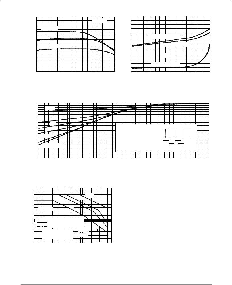
Figure 3. DC Current Gain |
Figure 4. ªOnº Voltages |
|
|
1 |
|
|
|
|
|
|
|
|
|
|
|
|
|
|
|
|
|
|
|
|
|
0.7 |
D = 0.5 |
|
|
|
|
|
|
|
|
|
|
|
|
|
|
|
|
|
|
|
RESISTANCE(NORMALIZED) |
0.5 |
|
|
|
|
|
|
|
|
|
|
|
|
|
|
|
|
|
|
|
r(t), TRANSIENT THERMAL |
0.3 |
0.2 |
|
|
|
|
|
|
|
|
|
|
|
|
|
|
|
|
|
|
|
0.2 |
0.1 |
|
|
|
|
|
|
|
|
|
|
|
|
|
|
|
|
|
|
||
|
|
|
|
|
|
|
|
|
|
|
|
|
P(pk) |
|
|
|
|
||||
0.1 |
0.05 |
|
|
|
|
|
|
|
RθJC(t) = r(t) RθJC |
|
|
|
|
|
|
||||||
|
|
|
|
|
|
|
|
RθJC = 8.33°C/W MAX |
|
|
|
|
|
|
|
|
|||||
0.07 |
|
|
|
|
|
|
|
|
|
|
|
|
|
|
|
|
|||||
0.02 |
|
|
|
|
|
|
|
D CURVES APPLY FOR POWER |
|
|
|
|
|
|
|||||||
0.05 |
|
0.01 |
|
|
|
|
|
|
PULSE TRAIN SHOWN |
|
|
|
t1 |
|
|
|
|
||||
|
|
|
|
|
|
|
|
READ TIME AT t1 |
|
|
|
|
|
|
|
|
|||||
0.03 |
SINGLE PULSE |
|
|
|
|
|
|
|
|
|
|
t2 |
|
|
|
|
|||||
|
|
0.02 |
|
|
|
|
|
|
|
|
TJ(pk) ± TC = P(pk) θJC(t) |
|
|
|
DUTY CYCLE, D = t1/t2 |
|
|
||||
|
|
|
|
|
|
|
|
|
|
|
|
|
|
|
|
|
|
||||
|
|
0.01 |
0.02 0.03 |
0.05 |
0.1 |
0.2 |
0.3 |
0.5 |
1 |
2 |
3 |
5 |
10 |
20 |
30 |
50 |
100 |
200 |
300 |
500 |
|
|
|
0.01 |
1 k |
||||||||||||||||||
t, TIME (ms)
Figure 5. Thermal Response
|
5 |
|
|
|
|
|
|
|
(AMP) |
2 |
|
1 ms |
|
100 μs |
|
|
|
1 |
|
|
500 μs |
|
|
|
||
|
|
|
|
|
|
|
||
CURRENT |
0.5 |
TC ≤ 25°C |
dc |
|
|
|
|
|
|
|
|
|
|
||||
0.2 |
|
|
|
|
|
|||
|
|
|
|
|
|
|
||
,COLLECTOR |
|
|
|
|
|
|
|
|
0.1 |
|
SECOND BREAKDOWN LIMIT |
|
|
|
|||
0.05 |
|
THERMAL LIMIT @ 25°C |
|
|
|
|||
|
WIRE BOND LIMIT |
|
|
|
|
|
||
|
|
|
|
|
|
|
||
0.02 |
|
|
|
MJD47 |
|
|
|
|
C |
CURVES APPLY BELOW |
|
|
|
||||
I |
|
MJD50 |
|
|
|
|||
|
0.01 |
RATED VCEO |
|
|
|
|
||
|
0.005 |
10 |
20 |
50 |
100 |
200 |
300 |
500 |
|
5 |
|||||||
VCE, COLLECTOR±EMITTER VOLTAGE (VOLTS)
Figure 6. Active Region Safe Operating Area
There are two limitations on the power handling ability of a transistor: average junction temperature and second breakdown. Safe operating area curves indicate IC ± VCE limits of the transistor that must be observed for reliable operation; i.e., the transistor must not be subjected to greater dissipation than the curves indicate.
The data of Figure 6 is based on TJ(pk) = 150_C; TC is variable depending on conditions. Second breakdown pulse
limits are valid for duty cycles to 10% provided TJ(pk) v 150_C. TJ(pk) may be calculated from the data in Figure 5. At high case temperatures, thermal limitations will re-
duce the power that can be handled to values less than the limitations imposed by second breakdown.
Motorola Bipolar Power Transistor Device Data |
3 |

MJD47 |
MJD50 |
|
|
|
|
|
|
|
|
|
|
|
|
|
|
|
1 |
|
|
|
|
|
|
|
5 |
|
|
|
|
|
|
|
0.5 |
|
|
|
TJ = 25°C |
|
|
|
|
|
|
|
t |
|
|
|
|
|
|
VCC = 200 V |
|
|
2 |
|
|
|
s |
|
|
||
|
|
|
|
|
|
|
|
|
|
|
|
|
|||
|
|
|
|
tr |
IC/IB = 5 |
|
|
|
|
|
|
|
|
|
|
μs) |
0.2 |
|
|
|
|
|
μs) |
1 |
|
|
|
|
TJ = 25°C |
|
|
|
|
|
|
|
|
|
|
|
|
|
|
|
|||
( |
|
|
|
td |
|
|
|
( |
|
|
|
|
|
VCC = 200 V |
|
TIME |
0.1 |
|
|
|
|
|
TIME |
0.5 |
|
|
|
|
|
||
|
|
|
|
|
|
|
|
|
|
|
|
IC/IB = 5 |
|
||
t, |
0.05 |
|
|
|
|
|
|
t, |
|
|
|
|
|
|
|
|
|
|
|
|
|
|
|
0.2 |
|
|
|
tf |
|
|
|
|
|
|
|
|
|
|
|
|
|
|
|
|
|
||
|
0.02 |
|
|
|
|
|
|
|
0.1 |
|
|
|
|
|
|
|
0.01 |
|
|
|
|
|
|
|
0.05 |
|
|
|
|
|
|
|
0.02 |
0.05 |
0.1 |
0.2 |
0.5 |
1 |
2 |
|
0.02 |
0.05 |
0.1 |
0.2 |
0.5 |
1 |
2 |
IC, COLLECTOR CURRENT (AMPS) |
IC, COLLECTOR CURRENT (AMPS) |
Figure 7. Turn±On Time |
Figure 8. Turn-Off Time |
4 |
Motorola Bipolar Power Transistor Device Data |

MJD47 MJD50
PACKAGE DIMENSIONS
|
|
|
±T± |
SEATING |
|
|
|
|
PLANE |
|
B |
|
C |
|
V |
R |
|
E |
|
|
4 |
|
|
Z |
|
|
|
A |
|
S |
|
|
|
|
|
|
|
|
|
1 |
2 |
3 |
|
U |
|
|
|
K |
|
|
|
|
|
|
F |
|
|
J |
|
|
|
L |
H |
|
|
|
|
|
D 2 PL
G |
0.13 (0.005) M T |
NOTES:
1.DIMENSIONING AND TOLERANCING PER ANSI Y14.5M, 1982.
2.CONTROLLING DIMENSION: INCH.
|
INCHES |
MILLIMETERS |
||
DIM |
MIN |
MAX |
MIN |
MAX |
A |
0.235 |
0.250 |
5.97 |
6.35 |
B |
0.250 |
0.265 |
6.35 |
6.73 |
C |
0.086 |
0.094 |
2.19 |
2.38 |
D |
0.027 |
0.035 |
0.69 |
0.88 |
E |
0.033 |
0.040 |
0.84 |
1.01 |
F |
0.037 |
0.047 |
0.94 |
1.19 |
G |
0.180 BSC |
4.58 BSC |
||
H |
0.034 |
0.040 |
0.87 |
1.01 |
J |
0.018 |
0.023 |
0.46 |
0.58 |
K |
0.102 |
0.114 |
2.60 |
2.89 |
L |
0.090 BSC |
2.29 BSC |
||
R |
0.175 |
0.215 |
4.45 |
5.46 |
S |
0.020 |
0.050 |
0.51 |
1.27 |
U |
0.020 |
±±± |
0.51 |
±±± |
V |
0.030 |
0.050 |
0.77 |
1.27 |
Z |
0.138 |
±±± |
3.51 |
±±± |
STYLE 1:
PIN 1. BASE
2.COLLECTOR
3.EMITTER
4.COLLECTOR
|
|
|
CASE 369A±13 |
|
|
|
|
|
|
|
|
|
|
|
ISSUE W |
|
|
|
|
|
|
|
|
|
B |
|
C |
NOTES: |
|
|
|
|
|
|
|
|
|
|
|
|
|
|
|
|
|
||
V |
R |
|
E |
1. DIMENSIONING AND TOLERANCING PER ANSI |
|||||||
|
2. |
Y14.5M, 1982. |
|
|
|
||||||
|
|
|
|
CONTROLLING DIMENSION: INCH. |
|
||||||
|
4 |
|
|
|
|
|
|
INCHES |
MILLIMETERS |
||
|
|
|
|
DIM |
MIN |
MAX |
MIN |
MAX |
|||
|
|
|
|
|
|||||||
|
|
A |
|
|
A |
|
0.235 |
0.250 |
5.97 |
6.35 |
|
|
|
|
|
B |
|
0.250 |
0.265 |
6.35 |
6.73 |
||
1 |
2 |
3 |
|
|
C |
|
0.086 |
0.094 |
2.19 |
2.38 |
|
S |
|
|
|
|
D |
|
0.027 |
0.035 |
0.69 |
0.88 |
|
|
|
|
|
E |
|
0.033 |
0.040 |
0.84 |
1.01 |
||
±T± |
|
|
|
|
F |
|
0.037 |
0.047 |
0.94 |
1.19 |
|
|
|
|
|
G |
|
0.090 BSC |
2.29 BSC |
||||
SEATING |
|
K |
|
|
|
||||||
|
|
|
H |
|
0.034 |
0.040 |
0.87 |
1.01 |
|||
PLANE |
|
|
|
|
J |
|
0.018 |
0.023 |
0.46 |
0.58 |
|
|
|
|
|
|
|
||||||
|
|
|
|
|
K |
|
0.350 |
0.380 |
8.89 |
9.65 |
|
|
|
|
J |
|
R |
|
0.175 |
0.215 |
4.45 |
5.46 |
|
F |
|
|
|
S |
|
0.050 |
0.090 |
1.27 |
2.28 |
||
|
|
H |
|
V |
|
0.030 |
0.050 |
0.77 |
1.27 |
||
|
|
|
|
|
|||||||
|
|
D 3 PL |
|
|
STYLE 1: |
|
|
|
|
||
|
G |
0.13 (0.005) M |
T |
|
|
|
|
|
|||
|
|
|
PIN 1. |
BASE |
|
|
|||||
|
|
|
|
|
|
|
2. |
COLLECTOR |
|
|
|
|
|
|
|
|
|
|
3. |
EMITTER |
|
|
|
|
|
|
|
|
|
|
4. |
COLLECTOR |
|
|
|
CASE 369±07
ISSUE K
Motorola Bipolar Power Transistor Device Data |
5 |

MJD47 MJD50
Motorola reserves the right to make changes without further notice to any products herein. Motorola makes no warranty, representation or guarantee regarding the suitability of its products for any particular purpose, nor does Motorola assume any liability arising out of the application or use of any product or circuit, and specifically disclaims any and all liability, including without limitation consequential or incidental damages. ªTypicalº parameters can and do vary in different applications. All operating parameters, including ªTypicalsº must be validated for each customer application by customer's technical experts. Motorola does not convey any license under its patent rights nor the rights of others. Motorola products are not designed, intended, or authorized for use as components in systems intended for surgical implant into the body, or other applications intended to support or sustain life, or for any other application in which the failure of the Motorola product could create a situation where personal injury or death may occur. Should Buyer purchase or use Motorola products for any such unintended or unauthorized application, Buyer shall indemnify and hold Motorola and its officers, employees, subsidiaries, affiliates, and distributors harmless against all claims, costs, damages, and expenses, and reasonable attorney fees arising out of, directly or indirectly, any claim of personal injury or death associated with such unintended or unauthorized use, even if such claim alleges that Motorola was negligent regarding the design or manufacture of the part. Motorola and  are registered trademarks of Motorola, Inc. Motorola, Inc. is an Equal Opportunity/Affirmative Action Employer.
How to reach us: |
|
USA / EUROPE: Motorola Literature Distribution; |
JAPAN: Nippon Motorola Ltd.; Tatsumi±SPD±JLDC, Toshikatsu Otsuki, |
P.O. Box 20912; Phoenix, Arizona 85036. 1±800±441±2447 |
6F Seibu±Butsuryu±Center, 3±14±2 Tatsumi Koto±Ku, Tokyo 135, Japan. 03±3521±8315 |
MFAX: RMFAX0@email.sps.mot.com ± TOUCHTONE (602) 244±6609 HONG KONG: Motorola Semiconductors H.K. Ltd.; 8B Tai Ping Industrial Park, |
|
INTERNET: http://Design±NET.com |
51 Ting Kok Road, Tai Po, N.T., Hong Kong. 852±26629298 |
◊ MJD47/D
*MJD47/D*