

MOTOROLA
SEMICONDUCTOR TECHNICAL DATA
Order this document by MJL21193/D
Silicon Power Transistors
The MJL21193 and MJL21194 utilize Perforated Emitter technology and are specifically designed for high power audio output, disk head positioners and linear applications.
•Total Harmonic Distortion Characterized
•High DC Current Gain ± hFE = 25 Min @ IC = 8 Adc
•Excellent Gain Linearity
•High SOA: 2.25 A, 80 V, 1 Second
PNP
MJL21193*
NPN
MJL21194*
*Motorola Preferred Device
16 AMPERE
COMPLEMENTARY SILICON POWER TRANSISTORS 250 VOLTS
200 WATTS
CASE 340G±02
TO±3PBL
MAXIMUM RATINGS
Rating |
Symbol |
Value |
Unit |
|
|
|
|
Collector±Emitter Voltage |
VCEO |
250 |
Vdc |
Collector±Base Voltage |
VCBO |
400 |
Vdc |
Emitter±Base Voltage |
VEBO |
5 |
Vdc |
Collector±Emitter Voltage ± 1.5 V |
VCEX |
400 |
Vdc |
Collector Current Ð Continuous |
IC |
16 |
Adc |
Collector Current Ð Peak (1) |
|
30 |
|
Base Current ± Continuous |
IB |
5 |
Adc |
Total Power Dissipation @ TC = 25°C |
PD |
200 |
Watts |
Derate Above 25°C |
|
1.43 |
W/°C |
|
|
|
|
Operating and Storage Junction Temperature Range |
TJ, Tstg |
± 65 to +150 |
°C |
THERMAL CHARACTERISTICS
Characteristic |
|
|
Symbol |
Max |
Unit |
|
|
|
|
|
|
Thermal Resistance, Junction to Case |
|
|
RθJC |
0.7 |
°C/W |
ELECTRICAL CHARACTERISTICS (TC = 25°C unless otherwise noted) |
|
|
|
|
|
Characteristic |
Symbol |
Min |
Typical |
Max |
Unit |
|
|
|
|
|
|
OFF CHARACTERISTICS |
|
|
|
|
|
|
|
|
|
|
|
Collector±Emitter Sustaining Voltage |
VCEO(sus) |
250 |
Ð |
Ð |
Vdc |
(IC = 100 mAdc, IB = 0) |
|
|
|
|
|
Collector Cutoff Current |
ICEO |
Ð |
Ð |
100 |
μAdc |
(VCE = 200 Vdc, IB = 0) |
|
|
|
|
|
(1) Pulse Test: Pulse Width = 5.0 μs, Duty Cycle ≤ 10%. |
|
|
|
|
(continued) |
Preferred devices are Motorola recommended choices for future use and best overall value.
Motorola, Inc. 1995
MJL21193 |
MJL21194 |
|
|
|
|
|
|
|
|
ELECTRICAL CHARACTERISTICS (TC = 25°C unless otherwise noted) |
|
|
|
|
|
||
|
|
Characteristic |
|
Symbol |
Min |
Typical |
Max |
Unit |
|
|
|
|
|
|
|
|
|
|
OFF CHARACTERISTICS |
|
|
|
|
|
|
|
|
|
|
|
|
|
|
|
|
|
Emitter Cutoff Current |
|
IEBO |
Ð |
Ð |
100 |
μAdc |
|
|
(VCE = 5 Vdc, IC = 0) |
|
|
|
|
|
|
|
|
Collector Cutoff Current |
|
ICEX |
Ð |
Ð |
100 |
μAdc |
|
|
(VCE = 250 Vdc, VBE(off) = 1.5 Vdc) |
|
|
|
|
|
|
|
|
SECOND BREAKDOWN |
|
|
|
|
|
|
|
|
|
|
|
|
|
|
||
|
Second Breakdown Collector Current with Base Forward Biased |
IS/b |
|
|
|
Adc |
||
|
(VCE = 50 Vdc, t = 1 s (non±repetitive) |
|
|
4.0 |
Ð |
Ð |
|
|
|
(VCE = 80 Vdc, t = 1 s (non±repetitive) |
|
|
2.25 |
Ð |
Ð |
|
|
|
ON CHARACTERISTICS |
|
|
|
|
|
|
|
|
|
|
|
|
|
|
|
|
|
DC Current Gain |
|
hFE |
|
|
|
|
|
|
(IC = 8 Adc, VCE = 5 Vdc) |
|
|
25 |
Ð |
75 |
|
|
|
(IC = 16 Adc, IB = 5 Adc) |
|
|
8 |
Ð |
Ð |
|
|
|
Base±Emitter On Voltage |
|
VBE(on) |
Ð |
Ð |
2.2 |
Vdc |
|
|
(IC = 8 Adc, VCE = 5 Vdc) |
|
|
|
|
|
|
|
|
Collector±Emitter Saturation Voltage |
|
VCE(sat) |
|
|
|
Vdc |
|
|
(IC = 8 Adc, IB = 0.8 Adc) |
|
|
Ð |
Ð |
1.4 |
|
|
|
(IC = 16 Adc, IB = 3.2 Adc) |
|
|
Ð |
Ð |
4 |
|
|
|
DYNAMIC CHARACTERISTICS |
|
|
|
|
|
|
|
|
|
|
|
|
|
|
|
|
|
Total Harmonic Distortion at the Output |
|
THD |
|
|
|
% |
|
|
VRMS = 28.3 V, f = 1 kHz, PLOAD = 100 WRMS |
hFE |
|
|
|
|
|
|
|
|
|
unmatched |
|
Ð |
0.8 |
Ð |
|
|
(Matched pair hFE = 50 @ 5 A/5 V) |
hFE |
|
|
|
|
|
|
|
|
|
matched |
|
Ð |
0.08 |
Ð |
|
|
|
|
|
|
|
|
|
|
|
Current Gain Bandwidth Product |
|
fT |
4 |
Ð |
Ð |
MHz |
|
|
(IC = 1 Adc, VCE = 10 Vdc, ftest = 1 MHz) |
|
|
|
|
|
|
|
|
Output Capacitance |
|
Cob |
Ð |
Ð |
500 |
pF |
|
|
(VCB = 10 Vdc, IE = 0, ftest = 1 MHz) |
|
|
|
|
|
|
|
|
(1) Pulse Test: Pulse Width = 300 μs, Duty Cycle ≤2% |
|
|
|
|
|
|
|
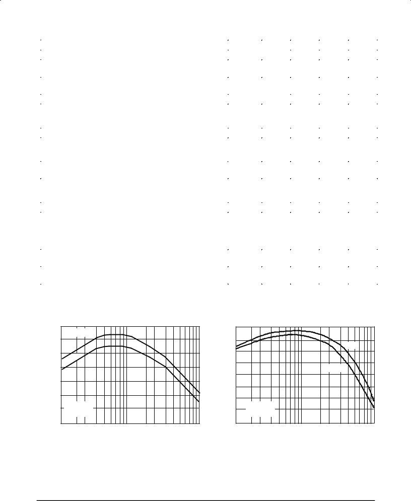
PNP MJL21193
(MHz) |
6.5 |
VCE = 10 V |
|
6.0 |
|
||
PRODUCT |
|
|
|
5.5 |
5 V |
|
|
|
|
||
GAIN BANDWIDTH |
|
|
|
5.0 |
|
|
|
4.5 |
|
|
|
4.0 |
|
|
|
, CURRENT |
3.5 |
TJ = 25°C |
|
|
ftest = 1 MHz |
|
|
3.0 |
|
|
|
T |
|
|
|
f |
1.0 |
10 |
|
|
0.1 |
IC COLLECTOR CURRENT (AMPS)
Figure 1. Typical Current Gain
Bandwidth Product
|
|
NPN MJL21194 |
|
(MHz) |
8.0 |
|
|
|
|
|
|
PRODUCT |
7.0 |
|
|
6.0 |
|
10 V |
|
|
|
||
|
|
|
|
BANDWIDTH |
5.0 |
VCE = 5 V |
|
4.0 |
|
||
|
|
||
3.0 |
|
|
|
GAIN |
|
|
|
2.0 |
|
|
|
, CURRENT |
|
|
|
1.0 |
TJ = 25°C |
|
|
ftest = 1 MHz |
|
||
|
|
||
0 |
|
|
|
T |
|
|
|
f |
1.0 |
10 |
|
|
0.1 |
IC COLLECTOR CURRENT (AMPS)
Figure 2. Typical Current Gain
Bandwidth Product
2 |
Motorola Bipolar Power Transistor Device Data |

1000
GAIN |
|
CURRENTDC, |
100 |
|
|
FE |
|
h |
|
|
10 |
|
0.1 |
1000
GAIN |
|
CURRENTDC, |
100 |
|
|
FE |
|
h |
|
|
10 |
|
0.1 |
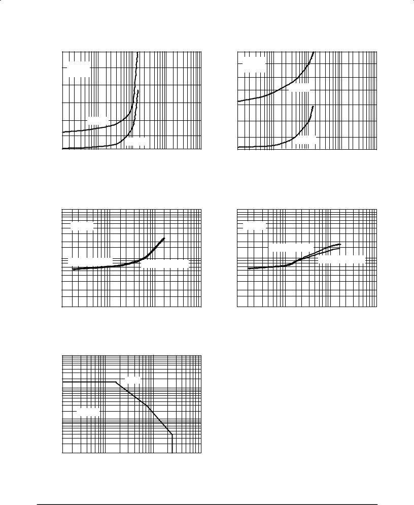
MJL21193 MJL21194
TYPICAL CHARACTERISTICS
PNP MJL21193
TJ = 100°C
25°C
± 25°C
VCE = 20 V
1.0 10 100
IC COLLECTOR CURRENT (AMPS)
Figure 3. DC Current Gain, VCE = 20 V
PNP MJL21193
TJ = 100°C
25°C
± 25°C
VCE = 5 V
1.0 10 100
IC COLLECTOR CURRENT (AMPS)
Figure 5. DC Current Gain, VCE = 5 V
NPN MJL21194
1000
GAIN |
TJ = 100°C |
CURRENT |
25°C |
|
|
|
100 |
, DC |
± 25°C |
|
|
FE |
|
h |
|
VCE = 20 V
10
0.1 1.0 10 100 IC COLLECTOR CURRENT (AMPS)
Figure 4. DC Current Gain, VCE = 20 V
NPN MJL21194
1000
GAIN |
|
|
TJ = 100°C |
|
CURRENT |
|
|
25°C |
|
|
|
|
|
|
|
100 |
|
|
|
, DC |
|
|
|
± 25°C |
|
|
|
|
|
FE |
|
|
|
|
h |
|
|
|
|
|
|
VCE = 20 V |
|
|
|
10 |
|
|
|
|
0.1 |
1.0 |
10 |
100 |
IC COLLECTOR CURRENT (AMPS)
Figure 6. DC Current Gain, VCE = 5 V
|
|
|
PNP MJL21193 |
|
|
|
|
30 |
|
|
|
|
|
|
25 |
|
1.5 A |
|
IB = 2 A |
|
(A) |
|
|
|
(A) |
||
|
|
|
|
|||
|
|
|
|
|
||
CURRENT |
20 |
|
|
|
1 A |
CURRENT |
|
|
|
|
|
||
COLLECTOR, |
|
|
|
|
COLLECTOR, |
|
15 |
|
|
|
0.5 A |
||
|
|
|
|
|
||
|
|
|
|
|
|
|
|
10 |
|
|
|
|
|
C |
5.0 |
|
|
|
|
C |
I |
|
|
|
|
I |
|
|
|
|
|
|
TJ = 25°C |
|
|
0 |
|
|
|
|
|
|
0 |
5.0 |
10 |
15 |
20 |
25 |
|
|
VCE, COLLECTOR±EMITTER VOLTAGE (VOLTS) |
|
|||
NPN MJL21194
35
IB = 2 A
30
1.5 A
25
|
1 A |
20 |
|
15 |
0.5 A |
10 |
|
5.0
|
|
|
|
TJ = 25°C |
|
0 |
|
|
|
|
|
0 |
5.0 |
10 |
15 |
20 |
25 |
VCE, COLLECTOR±EMITTER VOLTAGE (VOLTS)
Figure 7. Typical Output Characteristics |
Figure 8. Typical Output Characteristics |
Motorola Bipolar Power Transistor Device Data |
3 |
MJL21193 MJL21194
TYPICAL CHARACTERISTICS
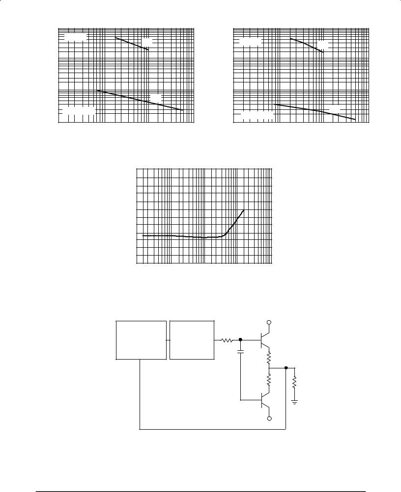
SATURATION VOLTAGE (VOLTS)
VBE(on)
, BASE±EMITTER VOLTAGE (VOLTS)
|
PNP MJL21193 |
|
|
|
NPN MJL21194 |
|
||
3.0 |
|
|
|
|
1.4 |
|
|
|
2.5 |
TJ = 25°C |
|
|
(VOLTS) |
1.2 |
TJ = 25°C |
|
|
|
|
|
IC/IB = 10 |
|
|
|||
|
IC/IB = 10 |
|
|
1.0 |
|
|
|
|
|
|
|
|
|
|
|
||
|
|
|
|
|
|
|
|
|
2.0 |
|
|
|
VOLTAGE |
0.8 |
|
VBE(sat) |
|
1.5 |
|
|
|
|
|
|||
|
|
|
|
|
|
|
||
|
|
|
|
SATURATION |
0.6 |
|
|
|
1.0 |
VBE(sat) |
|
|
0.4 |
|
|
|
|
|
|
|
|
|
|
|||
0.5 |
|
VCE(sat) |
|
|
0.2 |
|
VCE(sat) |
|
0 |
|
|
|
0 |
|
|
||
0.1 |
1.0 |
10 |
100 |
|
0.1 |
1.0 |
10 |
100 |
|
IC, COLLECTOR CURRENT (AMPS) |
|
|
|
IC, COLLECTOR CURRENT (AMPS) |
|
||
|
Figure 9. Typical Saturation Voltages |
|
|
|
Figure 10. Typical Saturation Voltages |
|
||
|
PNP MJL21193 |
|
|
|
NPN MJL21194 |
|
||
10 |
|
|
|
(VOLTS) |
10 |
|
|
|
|
TJ = 25°C |
|
|
|
TJ = 25°C |
|
|
|
|
|
|
VOLTAGE |
|
|
|
||
|
|
|
|
|
VCE = 20 V (SOLID) |
|
||
|
|
|
|
BASE±EMITTER, |
|
|
||
1.0 |
VCE = 20 V (SOLID) |
VCE = 5 V (DASHED) |
|
1.0 |
|
VCE = 5 V (DASHED) |
|
|
|
|
|
|
|||||
|
|
|
|
|
|
|||
|
|
|
|
|
|
|
||
|
|
|
|
BE(on) |
|
|
|
|
0.1 |
|
|
|
V |
0.1 |
|
|
|
|
|
|
|
|
|
|
||
0.1 |
1.0 |
10 |
100 |
|
0.1 |
1.0 |
10 |
100 |
|
IC, COLLECTOR CURRENT (AMPS) |
|
|
|
IC, COLLECTOR CURRENT (AMPS) |
|
||
|
Figure 11. Typical Base±Emitter Voltage |
|
|
|
Figure 12. Typical Base±Emitter Voltage |
|
||
|
100 |
|
|
|
(AMPS) |
|
|
1 SEC |
|
CURRENT |
|
|
|
|
10 |
|
|
|
|
|
|
|
|
|
, COLLECTOR |
1.0 |
TC = 25°C |
|
|
|
|
|
||
|
|
|
|
|
C |
|
|
|
|
I |
|
|
|
|
|
0.1 |
|
|
|
|
1.0 |
10 |
100 |
1000 |
|
|
VCE, COLLECTOR±EMITTER VOLTAGE (VOLTS) |
|
|
Figure 13. Active Region Safe Operating Area
There are two limitations on the power handling ability of a transistor; average junction temperature and secondary breakdown. Safe operating area curves indicate IC ± VCE limits of the transistor that must be observed for reliable operation; i.e., the transistor must not be subjected to greater dissipation than the curves indicate.
The data of Figure 13 is based on TJ(pk) = 200°C; TC is variable depending on conditions. At high case tempera-
tures, thermal limitations will reduce the power than can be handled to values less than the limitations imposed by second breakdown.
4 |
Motorola Bipolar Power Transistor Device Data |
|
10000 |
|
|
|
|
|
TC = 25°C |
Cib |
|
|
|
|
|
|
CAPACITANCE (pF) |
1000 |
|
|
|
C, |
|
|
|
Cob |
|
|
|
|
|
|
|
f(test) = 1 MHz) |
|
|
|
100 |
|
|
|
|
0.1 |
1.0 |
10 |
100 |
VR, REVERSE VOLTAGE (VOLTS)
Figure 14. MJL21193 Typical Capacitance
C, CAPACITANCE (pF)
|
MJL21193 |
MJL21194 |
10000 |
|
|
TC = 25°C |
Cib |
|
|
|
1000
Cob
f(test) = 1 MHz)
100
0.1 1.0 10 10
VR, REVERSE VOLTAGE (VOLTS)
Figure 15. MJL21194 Typical Capacitance
|
|
1.2 |
|
|
|
|
|
|
1.1 |
|
|
|
|
, TOTAL HARMONIC |
DISTORTION (%) |
1.0 |
|
|
|
|
0.9 |
|
|
|
|
||
0.8 |
|
|
|
|
||
HD |
|
|
|
|
|
|
|
|
|
|
|
|
|
T |
|
|
|
|
|
|
|
|
0.7 |
|
|
|
|
|
|
0.6 |
|
|
|
|
|
|
10 |
100 |
1000 |
10000 |
100000 |
FREQUENCY (Hz)
Figure 16. Typical Total Harmonic Distortion
|
|
+50 V |
AUDIO PRECISION |
|
|
MODEL ONE PLUS |
SOURCE |
50 Ω |
TOTAL HARMONIC |
AMPLIFIER |
DUT |
DISTORTION |
|
|
ANALYZER |
|
0.5 Ω |
|
|
0.5 Ω |
8.0 |
Ω |
|
||
DUT |
|
|
±50 V |
|
|
Figure 17. Total Harmonic Distortion Test Circuit
Motorola Bipolar Power Transistor Device Data |
5 |
MJL21193 MJL21194
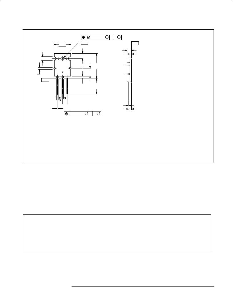
PACKAGE DIMENSIONS
|
|
0.25 (0.010) M |
T B M |
|
±B± |
±Q± |
±T± |
|
|
|
|
|
|
|
C |
|
|
U |
E |
|
N |
|
|
|
|
|
|
|
|
A |
|
R |
1 2 3 |
L |
|
|
|
±Y± 
 P
P
K
W
F 2 PL
 G
G 
J
D 3 PL |
H |
|
0.25 (0.010) M Y Q S
NOTES:
1.DIMENSIONING AND TOLERANCING PER ANSI Y14.5M, 1982.
2.CONTROLLING DIMENSION: MILLIMETER.
|
MILLIMETERS |
INCHES |
||
DIM |
MIN |
MAX |
MIN |
MAX |
A |
2.8 |
2.9 |
1.102 |
1.142 |
B |
19.3 |
20.3 |
0.760 |
0.800 |
C |
4.7 |
5.3 |
0.185 |
0.209 |
D |
0.93 |
1.48 |
0.037 |
0.058 |
E |
1.9 |
2.1 |
0.075 |
0.083 |
F |
2.2 |
2.4 |
0.087 |
0.102 |
G |
5.45 BSC |
0.215 BSC |
||
H |
2.6 |
3.0 |
0.102 |
0.118 |
J |
0.43 |
0.78 |
0.017 |
0.031 |
K |
17.6 |
18.8 |
0.693 |
0.740 |
L |
11.0 |
11.4 |
0.433 |
0.449 |
N |
3.95 |
4.75 |
0.156 |
0.187 |
P |
2.2 |
2.6 |
0.087 |
0.102 |
Q |
3.1 |
3.5 |
0.122 |
0.137 |
R |
2.15 |
2.35 |
0.085 |
0.093 |
U |
6.1 |
6.5 |
0.240 |
0.256 |
W |
2.8 |
3.2 |
0.110 |
0.125 |
STYLE 2:
PIN 1. BASE
2.COLLECTOR
3.EMITTER
CASE 340G±02
TO±3PBL
ISSUE E
Motorola reserves the right to make changes without further notice to any products herein. Motorola makes no warranty, representation or guarantee regarding the suitability of its products for any particular purpose, nor does Motorola assume any liability arising out of the application or use of any product or circuit, and specifically disclaims any and all liability, including without limitation consequential or incidental damages. ªTypicalº parameters can and do vary in different applications. All operating parameters, including ªTypicalsº must be validated for each customer application by customer's technical experts. Motorola does not convey any license under its patent rights nor the rights of others. Motorola products are not designed, intended, or authorized for use as components in systems intended for surgical implant into the body, or other applications intended to support or sustain life, or for any other application in which the failure of the Motorola product could create a situation where personal injury or death may occur. Should Buyer purchase or use Motorola products for any such unintended or unauthorized application, Buyer shall indemnify and hold Motorola and its officers, employees, subsidiaries, affiliates, and distributors harmless against all claims, costs, damages, and expenses, and reasonable attorney fees arising out of, directly or indirectly, any claim of personal injury or death associated with such unintended or unauthorized use, even if such claim alleges that Motorola was negligent regarding the design or manufacture of the part. Motorola and  are registered trademarks of Motorola, Inc. Motorola, Inc. is an Equal Opportunity/Affirmative Action Employer.
How to reach us: |
|
USA / EUROPE: Motorola Literature Distribution; |
JAPAN: Nippon Motorola Ltd.; Tatsumi±SPD±JLDC, Toshikatsu Otsuki, |
P.O. Box 20912; Phoenix, Arizona 85036. 1±800±441±2447 |
6F Seibu±Butsuryu±Center, 3±14±2 Tatsumi Koto±Ku, Tokyo 135, Japan. 03±3521±8315 |
MFAX: RMFAX0@email.sps.mot.com ± TOUCHTONE (602) 244±6609 HONG KONG: Motorola Semiconductors H.K. Ltd.; 8B Tai Ping Industrial Park, |
|
INTERNET: http://Design±NET.com |
51 Ting Kok Road, Tai Po, N.T., Hong Kong. 852±26629298 |
◊ MJL21193/D
*MJL21193/D*