

MOTOROLA
SEMICONDUCTOR TECHNICAL DATA
Order this document by BUH51/D
|
|
|
BUH51 |
|
Advance |
Information |
|
||
|
||||
POWER TRANSISTOR |
||||
SWITCHMODE |
NPN Silicon |
|||
3 AMPERES |
||||
Planar |
Power |
Transistor |
800 VOLTS |
|
50 WATTS |
||||
|
|
|
||
|
|
|
|
|
The BUH51 has an application specific state±of±art die designed for use in 50 Watts Halogen electronic transformers.
This power transistor is specifically designed to sustain the large inrush current during either the start±up conditions or under a short circuit across the load.
This High voltage/High speed product exhibits the following main features:
•Improved Efficiency Due to the Low Base Drive Requirements:
ÐHigh and Flat DC Current Gain h FE
ÐFast Switching
•Robustness Thanks to the Technology Developed to Manufacture this Device
•Motorola ª6 SIGMAº Philosophy Providing Tight and Reproducible Parametric Distributions
MAXIMUM RATINGS
CASE 77±07
TO±225AA TYPE
Rating |
Symbol |
Value |
Unit |
|
|
|
|
Collector±Emitter Sustaining Voltage |
VCEO |
500 |
Vdc |
Collector±Base Breakdown Voltage |
VCBO |
800 |
Vdc |
Collector±Emitter Breakdown Voltage |
VCES |
800 |
Vdc |
Emitter±Base Voltage |
VEBO |
10 |
Vdc |
Collector Current Ð Continuous |
IC |
3 |
Adc |
Ð Peak (1) |
ICM |
8 |
|
Base Current Ð Continuous |
IB |
2 |
Adc |
Base Current Ð Peak (1) |
IBM |
4 |
|
*Total Device Dissipation @ TC = 25_C |
PD |
50 |
Watt |
*Derate above 25°C |
|
0.4 |
W/_C |
|
|
|
|
Operating and Storage Temperature |
TJ, Tstg |
± 65 to 150 |
_C |
THERMAL CHARACTERISTICS
Thermal Resistance |
|
|
_C/W |
Ð Junction to Case |
RqJC |
2.5 |
|
Ð Junction to Ambient |
RqJA |
100 |
|
Maximum Lead Temperature for Soldering Purposes: |
TL |
260 |
_C |
1/8″ from case for 5 seconds |
|
|
|
|
|
|
|
(1) Pulse Test: Pulse Width = 5 ms, Duty Cycle ≤ 10%. |
|
|
|
Designer's and SWITCHMODE are trademarks of Motorola, Inc.
This document contains information on a new product. Specifications and information herein are subject to change without notice.
Motorola, Inc. 1995

BUH51
ELECTRICAL CHARACTERISTICS (TC = 25°C unless otherwise noted)
|
|
Characteristic |
|
Symbol |
Min |
Typ |
Max |
Unit |
||
|
|
|
|
|
|
|
|
|
|
|
OFF CHARACTERISTICS |
|
|
|
|
|
|
|
|
|
|
|
|
|
|
|
|
|
|
|
|
|
Collector±Emitter Sustaining Voltage |
|
|
|
VCEO(sus) |
500 |
550 |
|
Vdc |
||
(IC = 100 mA, L = 25 mH) |
|
|
|
|
|
|
|
|
|
|
Collector±Base Breakdown Voltage |
|
|
|
VCBO |
800 |
950 |
|
Vdc |
||
(ICBO = 1 mA) |
|
|
|
|
|
|
|
|
|
|
Emitter±Base Breakdown Voltage |
|
|
|
VEBO |
10 |
12.5 |
|
Vdc |
||
(IEBO = 1 mA) |
|
|
|
|
|
|
|
|
|
|
Collector Cutoff Current |
|
|
|
|
ICEO |
|
|
100 |
μAdc |
|
(VCE = Rated VCEO, IB = 0) |
|
|
|
|
|
|
|
|
||
Collector Cutoff Current |
|
|
|
@ TC = 25°C |
ICES |
|
|
100 |
μAdc |
|
(VCE = Rated VCES, VEB = 0) |
|
|
@ TC = 125°C |
|
|
|
1000 |
|
||
Collector Base Current |
|
|
|
@ TC = 25°C |
ICBO |
|
|
100 |
μAdc |
|
(VCB = Rated VCBO, VEB = 0) |
|
|
@ TC = 125°C |
|
|
|
1000 |
|
||
Emitter±Cutoff Current |
|
|
|
|
IEBO |
|
|
100 |
μAdc |
|
(VEB = 9 Vdc, IC = 0) |
|
|
|
|
|
|
|
|
|
|
ON CHARACTERISTICS |
|
|
|
|
|
|
|
|
|
|
|
|
|
|
|
|
|
|
|
|
|
Base±Emitter Saturation Voltage |
|
|
@ TC = 25°C |
VBE(sat) |
|
0.92 |
1.1 |
Vdc |
||
(IC = 1 Adc, IB = 0.2 Adc) |
|
|
|
@ TC = 125°C |
|
|
0.8 |
|
|
|
Collector±Emitter Saturation Voltage |
|
|
@ TC = 25°C |
VCE(sat) |
|
0.3 |
0.5 |
Vdc |
||
(IC = 1 Adc, IB = 0.2 Adc) |
|
|
|
@ TC = 125°C |
|
|
0.32 |
0.6 |
|
|
DC Current Gain (IC = 1 Adc, VCE = 1 Vdc) |
@ TC = 25°C |
hFE |
8 |
10 |
|
Ð |
||||
|
|
|
|
|
@ TC = 125°C |
|
6 |
8 |
|
|
DC Current Gain (IC = 2 Adc, VCE = 5 Vdc) |
@ TC = 25°C |
|
5 |
7.5 |
|
Ð |
||||
|
|
|
|
|
@ TC = 125°C |
|
4 |
6.2 |
|
|
DC Current Gain (IC = 0.8 Adc, VCE = 5 Vdc) |
@ TC = 25°C |
|
10 |
14 |
|
Ð |
||||
|
|
|
|
|
@ TC = 125°C |
|
8 |
13 |
|
|
DC Current Gain (IC = 10 mAdc, VCE = 5 Vdc) |
@ TC = 25°C |
|
14 |
20 |
|
Ð |
||||
|
|
|
|
|
@ TC = 125°C |
|
18 |
25 |
|
|
DYNAMIC SATURATION VOLTAGE |
|
|
|
|
|
|
|
|
||
|
|
|
|
|
|
|
|
|
||
Dynamic Saturation |
|
I = 1 Adc, I = 0.2 Adc |
@ TC = 25°C |
VCE(dsat) |
|
1.7 |
|
V |
||
|
|
C |
|
B1 |
|
|
|
|
|
|
Voltage: |
|
VCC = 300 V |
@ T = 125°C |
|
|
6 |
|
V |
||
Determined 3 μs after |
|
|
|
|
C |
|
|
|
|
|
|
|
|
|
@ TC = 25°C |
|
|
5.1 |
|
V |
|
rising IB1 reaches |
|
IC = 2 Adc, IB1 = 0.4 Adc |
|
|
|
|||||
90% of final IB1 |
|
V |
CC |
= 300 V |
° |
|
|
15 |
|
V |
|
|
|
|
@ TC = 125 C |
|
|
|
|||
DYNAMIC CHARACTERISTICS |
|
|
|
|
|
|
|
|
||
|
|
|
|
|
|
|
|
|
|
|
Current Gain Bandwidth |
|
|
|
|
fT |
|
23 |
|
MHz |
|
(IC = 1 Adc, VCE = 10 Vdc, f = 1 MHz) |
|
|
|
|
|
|
|
|||
Output Capacitance |
|
|
|
|
Cob |
|
34 |
100 |
pF |
|
(VCB = 10 Vdc, IE = 0, f = 1 MHz) |
|
|
|
|
|
|
|
|
||
Input Capacitance |
|
|
|
|
Cib |
|
200 |
500 |
pF |
|
(VEB = 8 Vdc, f = 1 MHz) |
|
|
|
|
|
|
|
|
|
|
2 |
Motorola Bipolar Power Transistor Device Data |
|
|
|
|
|
|
|
|
|
|
BUH51 |
|
ELECTRICAL CHARACTERISTICS (TC = 25°C unless otherwise noted) |
|
|
|
|
|
|
|
||||
|
|
|
|
|
|
|
|
|
|
|
|
|
Characteristic |
|
|
Symbol |
|
Min |
Typ |
Max |
|
Unit |
|
|
|
|
|
|
|
|
|
|
|
||
SWITCHING CHARACTERISTICS: Resistive Load (D.C. ≤ 10%, Pulse Width = 40 μs) |
|
|
|
|
|
||||||
|
|
|
|
|
|
|
|
|
|
|
|
Turn±on Time |
I |
= 1 Adc, I |
= 0.2 Adc |
@ TC = 25°C |
ton |
|
|
110 |
150 |
|
ns |
|
° |
|
|
|
125 |
|
|
|
|||
|
C |
B1 |
|
@ TC = 125 C |
|
|
|
|
|
|
|
|
|
IB2 = 0.2 Adc |
|
|
|
|
|
|
|
|
|
Turn±off Time |
|
@ TC = 25°C |
toff |
|
|
3.5 |
4 |
|
μs |
||
|
VCC = 300 Vdc |
|
|
|
|||||||
|
|
|
|
@ TC = 125°C |
|
|
|
4.1 |
|
|
|
Turn±on Time |
I |
= 2 Adc, I |
= 0.4 Adc |
@ TC = 25°C |
ton |
|
|
700 |
1000 |
|
ns |
|
° |
|
|
|
1250 |
|
|
|
|||
|
C |
B1 |
|
@ TC = 125 C |
|
|
|
|
|
|
|
|
|
IB2 = 0.4 Adc |
|
|
|
|
|
|
|
|
|
Turn±off Time |
|
@ TC = 25°C |
toff |
|
|
1.75 |
2 |
|
μs |
||
|
VCC = 300 Vdc |
|
|
|
|||||||
|
|
|
|
@ TC = 125°C |
|
|
|
2.1 |
|
|
|
SWITCHING CHARACTERISTICS: Inductive Load (Vclamp = 300 V, VCC = 15 V, L = 200 μH) |
|
|
|
|
|
||||||
Fall Time |
|
|
|
@ TC = 25°C |
tfi |
|
|
200 |
300 |
|
ns |
|
|
|
|
@ TC = 125°C |
|
|
|
320 |
|
|
|
Storage Time |
|
IC = 1 Adc |
@ TC = 25°C |
tsi |
|
|
3.4 |
3.75 |
|
μs |
|
|
IB1 = 0.2 Adc |
|
|
|
|||||||
|
|
@ TC = 125°C |
|
|
|
4 |
|
|
|
||
|
|
IB2 = 0.2 Adc |
|
|
|
|
|
|
|||
Crossover Time |
|
|
|
@ TC = 25°C |
tc |
|
|
350 |
500 |
|
ns |
|
|
|
|
@ TC = 125°C |
|
|
|
640 |
|
|
|
Fall Time |
|
|
|
@ TC = 25°C |
tfi |
|
|
140 |
200 |
|
ns |
|
|
IC = 2 Adc |
@ TC = 125°C |
|
|
|
300 |
|
|
|
|
Storage Time |
|
@ TC = 25°C |
tsi |
|
|
2.3 |
2.75 |
|
μs |
||
|
IB1 = 0.4 Adc |
|
|
|
|||||||
|
|
@ TC = 125°C |
|
|
|
2.8 |
|
|
|
||
|
|
IB2 = 0.4 Adc |
|
|
|
|
|
|
|||
Crossover Time |
|
|
|
@ TC = 25°C |
tc |
|
|
400 |
600 |
|
ns |
|
|
|
|
@ TC = 125°C |
|
|
|
725 |
|
|
|
TYPICAL STATIC CHARACTERISTICS
|
100 |
|
|
|
|
|
|
|
|
|
|
|
VCE = 1 V |
GAIN |
|
|
TJ = 125°C |
|
|
|
|
|
|
|
|
|
|
CURRENT |
10 |
TJ = ± 20°C |
|
|
|
|
|
|
TJ = 25°C |
|
|
|
|
, DC |
|
|
|
|
|
|
FE |
|
|
|
|
|
|
h |
|
|
|
|
|
|
|
1 |
|
0.01 |
|
|
|
|
0.001 |
0.1 |
1 |
10 |
||
|
|
|
IC, COLLECTOR CURRENT (AMPS) |
|
||
Figure 1. DC Current Gain @ 1 Volt
|
100 |
|
|
|
|
|
|
|
|
|
|
|
VCE = 3 V |
GAIN |
|
|
TJ = 125°C |
|
|
|
|
|
|
|
|
|
|
, DC CURRENT |
10 |
TJ = ± 20°C |
TJ = 25°C |
|
|
|
|
|
|
|
|
|
|
FE |
|
|
|
|
|
|
h |
|
|
|
|
|
|
|
1 |
|
0.01 |
|
|
|
|
0.001 |
0.1 |
1 |
10 |
||
IC, COLLECTOR CURRENT (AMPS)
Figure 2. DC Current Gain @ 3 Volt
Motorola Bipolar Power Transistor Device Data |
3 |

BUH51
TYPICAL STATIC CHARACTERISTICS
|
100 |
|
|
|
|
|
|
|
|
|
|
|
VCE = 5 V |
GAIN |
|
TJ = 125°C |
|
|
|
|
|
|
|
|
|
|
|
, DC CURRENT |
10 |
TJ = ± 20°C |
|
TJ = 25°C |
|
|
|
|
|
|
|
|
|
FE |
|
|
|
|
|
|
h |
|
|
|
|
|
|
|
1 |
|
0.01 |
|
|
|
|
0.001 |
0.1 |
1 |
10 |
||
IC, COLLECTOR CURRENT (AMPS)
Figure 3. DC Current Gain @ 5 Volt
|
10 |
|
|
|
|
|
IC/IB = 10 |
|
|
|
|
(VOLTS) |
|
|
|
|
|
, VOLTAGE |
1 |
|
|
|
TJ = 25°C |
|
|
|
|
||
|
|
|
|
|
|
CE |
|
|
TJ = ± 20°C |
|
|
V |
|
|
|
|
|
|
TJ = 125°C |
|
|
|
|
|
0.1 |
|
|
|
|
|
0.001 |
0.01 |
0.1 |
1 |
10 |
|
|
IC, COLLECTOR CURRENT (AMPS) |
|
||
Figure 5. Collector±Emitter Saturation Voltage
|
1.5 |
|
|
|
|
|
|
|
|
IC/IB = 10 |
|
|
|
||
(VOLTS) |
1 |
|
|
|
|
|
|
|
|
|
|
|
|
|
|
VOLTAGE |
TJ = ± 20°C |
|
|
|
|||
0.5 |
T |
J |
= 25°C |
|
|
|
|
, |
|
|
|
|
|
||
BE |
|
|
|
|
|
|
|
|
|
|
TJ = 125°C |
|
|
|
|
V |
|
|
|
|
|
|
|
|
|
|
|
|
|
|
|
|
0 |
|
|
|
|
|
|
|
0.001 |
|
|
0.01 |
0.1 |
1 |
10 |
|
|
|
|
IC, COLLECTOR CURRENT (AMPS) |
|
||
Figure 7. Base±Emitter Saturation Region
|
10 |
|
|
|
|
|
|
IC/IB = 5 |
|
TJ = 125°C |
|
(VOLTS) |
|
|
|
|
|
1 |
|
|
|
|
|
|
|
TJ = 25°C |
|
|
|
VOLTAGE |
|
|
|
|
|
|
|
TJ = ± 20°C |
|
|
|
, |
0.1 |
|
|
|
|
CE |
|
|
|
|
|
|
|
|
|
|
|
V |
|
|
|
|
|
|
0.01 |
0.01 |
|
|
|
|
0.001 |
0.1 |
1 |
10 |
|
|
|
IC, COLLECTOR CURRENT (AMPS) |
|
||
Figure 4. Collector±Emitter Saturation Voltage
|
1.5 |
|
|
|
|
|
|
IC/IB = 5 |
|
|
|
(VOLTS) |
1 |
|
TJ = ± 20°C |
|
|
|
|
|
|
||
VOLTAGE |
|
|
|
|
|
0.5 |
TJ = 25°C |
|
|
|
|
, |
|
TJ = 125°C |
|
|
|
BE |
|
|
|
||
V |
|
|
|
|
|
|
0 |
|
|
|
|
|
0.001 |
0.01 |
0.1 |
1 |
10 |
IC, COLLECTOR CURRENT (AMPS)
Figure 6. Base±Emitter Saturation Region
|
2 |
|
|
|
|
|
|
|
TJ = 25°C |
|
|
|
|
4 A |
(VOLTS) |
1.5 |
|
3 A |
|
|
|
2 A |
|
|
|
|
|
|
|
VOLTAGE, |
1 |
1 A |
|
|
|
|
|
||
|
|
|
|
|
CE |
|
|
|
|
V |
0.5 |
|
|
|
|
|
|
|
|
|
VCE(sat) |
|
|
|
|
(IC = 500 mA) |
|
|
|
|
0 |
|
|
|
|
0.01 |
0.1 |
1 |
10 |
IB, BASE CURRENT (A)
Figure 8. Collector Saturation Region
4 |
Motorola Bipolar Power Transistor Device Data |
BUH51
TYPICAL STATIC CHARACTERISTICS
|
1000 |
|
|
|
|
TJ = 25°C |
|
|
|
f(test) = 1 MHz |
|
(pF) |
|
Cib |
|
C, CAPACITANCE |
100 |
|
|
|
|
|
|
|
|
Cob |
|
|
10 |
|
|
|
1 |
10 |
100 |
|
|
VR, REVERSE VOLTAGE (VOLTS) |
|
Figure 9. Capacitance
|
1000 |
|
|
|
|
|
900 |
|
|
TJ = 25°C |
|
|
|
|
|
|
|
(VOLTS) |
800 |
|
|
|
|
700 |
|
|
|
|
|
BVCER |
|
|
|
|
|
600 |
|
BVCER @ 10 mA |
|
|
|
|
|
|
|
|
|
|
500 |
BVCER(sus) @ 200 mA, 25 mH |
|
|
|
|
|
|
|
|
|
|
400 |
|
|
|
|
|
10 |
100 |
1000 |
10000 |
100000 |
|
|
|
RBE (Ω) |
|
|
Figure 10. Resistive Breakdown
TYPICAL SWITCHING CHARACTERISTICS
|
2500 |
|
|
|
|
|
|
|
IB1 = IB2 |
|
|
|
|
|
2000 |
VCC = 300 V |
IC/IB = 5 |
|
||
|
PW = 40 |
μ |
s |
|
||
|
|
|
|
|
||
t, TIME (ns) |
1500 |
|
|
|
|
|
1000 |
|
|
|
|
|
|
|
|
|
|
|
|
|
|
500 |
|
|
|
|
TJ = 125°C |
|
|
|
|
|
|
|
|
0 |
|
|
|
|
TJ = 25°C |
|
0 |
|
1 |
2 |
3 |
|
|
|
|
||||
IC, COLLECTOR CURRENT (AMPS)
|
10 |
|
|
|
|
|
|
|
IB1 = IB2 |
|
8 |
|
IC/IB = 5 |
VCC = 300 V |
|
|
PW = 40 μs |
||
μs) |
6 |
|
|
|
t, TIME ( |
4 |
|
|
|
|
|
|
|
|
|
2 |
TJ = 125°C |
|
|
|
|
|
|
|
|
|
TJ = 25°C |
|
|
|
0 |
|
|
|
|
0 |
1 |
2 |
3 |
IC, COLLECTOR CURRENT (AMPS)
Figure 11. Resistive Switching, ton |
Figure 12. Resistive Switch Time, toff |
7 |
|
|
IB1 = IB2 |
|
4 |
|
|
|
|
|
|
||
|
|
IC/IB = 5 |
VCC = 15 V |
|
|
|
|
|
VZ |
= 300 V |
|
|
|
|
|
|
|
3 |
||
|
|
|
LC = 200 μH |
|
||
5 |
|
|
|
|
||
|
|
|
|
|
|
|
μs) |
|
|
|
|
μs) |
|
( |
|
|
|
|
( |
2 |
t, TIME |
|
|
|
|
t, TIME |
|
|
|
|
|
|
||
3 |
|
|
|
|
|
|
|
|
|
|
|
|
1 |
|
TJ = 125°C |
|
|
|
|
|
1 |
TJ = 25°C |
|
|
|
|
0 |
|
|
2 |
|
|
||
0 |
1 |
|
|
3 |
|
|
|
|
IC/IB = 10 |
IB1 = IB2 |
|
|
|
VCC = 15 V |
|
|
|
VZ = 300 V |
|
|
|
LC = 200 μH |
|
TJ = 125°C |
|
|
|
TJ = 25°C |
|
|
0.5 |
1 |
1.5 |
2 |
IC, COLLECTOR CURRENT (AMPS) |
IC, COLLECTOR CURRENT (AMPS) |
Figure 13. Inductive Storage Time, tsi |
Figure 13 Bis. Inductive Storage Time, tsi |
Motorola Bipolar Power Transistor Device Data |
5 |

BUH51
TYPICAL SWITCHING CHARACTERISTICS
|
800 |
IB1 = IB2 |
|
|
|
|
|
|
|
|
|
||
|
|
VCC = 15 V |
|
tc |
|
|
|
|
V |
= 300 V |
|
|
|
|
600 |
Z |
= 200 μH |
|
|
|
|
L |
|
|
|
||
|
|
C |
|
|
|
|
(ns) |
|
|
|
|
|
tc |
t, TIME |
400 |
|
|
|
|
|
|
|
|
|
|
tfi |
|
|
|
|
|
|
|
|
|
200 |
|
|
|
|
|
|
|
|
TJ = 125°C |
|
|
tfi |
|
|
|
TJ = 25°C |
|
|
|
|
0 |
0.5 |
1 |
1.5 |
2 |
2.5 |
|
|
|||||
IC, COLLECTOR CURRENT (AMPS)
Figure 14. Inductive Storage Time,
|
|
tc & tfi @ IC/IB = 5 |
|
||
|
4 |
|
|
|
|
(μs) |
3 |
|
|
|
|
STORAGE TIME |
|
|
IC = 0.8 A |
|
|
|
|
|
|
||
2 |
IC = 2 A |
|
|
|
|
, |
|
I |
= I |
|
|
si |
|
|
|||
t |
|
|
B1 |
B2 |
|
|
|
TJ = 125°C |
VCC = 15 V |
|
|
|
|
VZ = 300 V |
|
||
|
|
TJ = 25°C |
|
||
|
1 |
LC = 200 μH |
|
||
|
2 |
4 |
6 |
8 |
10 |
hFE, FORCED GAIN
Figure 16. Inductive Storage Time
|
1000 |
IB1 = IB2 |
|
|
|
|
|
|
|
|
|
||
|
|
VCC = 15 V |
|
|
|
|
|
800 |
VZ = 300 V |
|
|
|
|
|
|
LC |
= 200 μH |
|
|
tc |
|
|
|
|
|
|
|
t, TIME (ns) |
600 |
|
|
|
|
|
400 |
|
|
|
tfi |
|
|
|
|
|
|
|
|
|
|
200 |
|
|
|
|
TJ = 125°C |
|
|
|
|
|
|
|
|
0 |
|
|
|
|
TJ = 25°C |
|
0.5 |
1 |
1.5 |
2 |
2.5 |
|
|
|
|||||
IC, COLLECTOR CURRENT (AMPS)
Figure 15. Inductive Storage Time,
|
|
|
|
tc & tfi @ IC/IB = 10 |
|
|
||
|
450 |
IBoff = IB2 |
|
|
|
|
|
|
|
400 |
|
|
|
|
|
|
|
|
VCC = 15 V |
|
|
|
|
|
|
|
|
|
|
|
|
|
|
|
|
|
350 |
VZ = 300 V |
|
|
|
|
|
|
(ns) |
300 |
LC = 200 μH |
|
|
|
|
|
|
|
|
|
|
|
|
|
||
|
|
|
|
|
|
|
|
|
TIME |
250 |
|
|
|
|
|
|
|
|
|
|
|
|
|
|
|
|
, FALL |
200 |
|
|
|
|
|
|
|
150 |
|
|
|
|
|
|
|
|
fi |
|
|
|
|
|
|
|
|
t |
|
|
|
|
|
|
|
|
|
100 |
|
|
|
|
IC = 0.8 A |
|
|
|
50 |
IC = 2 A |
|
TJ = 125°C |
|
|
|
|
|
|
|
|
|
|
|||
|
0 |
|
|
TJ = 25°C |
|
|
|
|
|
|
5 |
|
|
8 |
9 |
|
|
|
3 |
4 |
6 |
7 |
10 |
|||
hFE, FORCED GAIN
Figure 17. Inductive Fall Time
|
800 |
|
TJ = 125°C |
|
|
|
|
|
|
|
|
|
|
IC = 2 A |
|
||
|
700 |
|
TJ = 25°C |
|
|
|
||
(ns) |
600 |
|
|
|
|
|
|
|
TIME |
|
|
|
|
|
|
|
|
500 |
|
|
|
|
|
IB1 = IB2 |
|
|
, CROSSOVER |
|
|
|
|
|
VCC = 15 V |
|
|
|
|
|
|
|
|
VZ = 300 V |
|
|
400 |
|
|
|
|
|
LC = 200 μH |
|
|
300 |
|
|
|
|
|
|
|
|
c |
|
|
|
|
|
|
|
|
t |
|
|
|
|
|
|
|
|
|
200 |
|
|
|
|
|
IC = 0.8 A |
|
|
100 |
|
|
|
|
|
|
|
|
3 |
4 |
5 |
6 |
7 |
8 |
9 |
10 |
hFE, FORCED GAIN
Figure 18. Inductive Crossover Time
6 |
Motorola Bipolar Power Transistor Device Data |

BUH51
TYPICAL SWITCHING CHARACTERISTICS
VCE |
dyn 1 μs |
dyn 3 μs |
0 V |
90% IB |
1 μs |
3 μs |
IB |
TIME |
Figure 19. Dynamic Saturation Voltage
Measurements
10 |
|
|
|
|
|
|
|
|
9 |
IC |
|
|
|
|
90% IC |
|
|
8 |
|
|
|
t |
|
tfi |
|
|
|
|
|
|
|
|
|
||
7 |
|
|
|
si |
|
|
|
|
|
|
|
|
|
|
|
|
|
6 |
|
|
10% Vclamp |
|
|
10% IC |
|
|
5 |
Vclamp |
|
|
t |
|
|||
|
|
|
|
|
|
c |
|
|
4 |
|
|
|
|
|
|
|
|
3 |
IB |
90% IB1 |
|
|
|
|
|
|
2 |
|
|
|
|
|
|
|
|
1 |
|
|
|
|
|
|
|
|
0 |
1 |
2 |
3 |
4 |
5 |
6 |
7 |
8 |
0 |
||||||||
|
|
|
|
TIME |
|
|
|
|
Figure 20. Inductive Switching Measurements
|
|
|
Table 1. Inductive Load Switching Drive Circuit |
|
|
|||
+15 V |
|
|
|
|
|
|
|
|
|
|
|
|
|
100 |
μF |
IC PEAK |
|
1 μF |
150 Ω |
100 Ω |
|
MTP8P10 |
|
|
||
|
|
|
|
|
||||
|
3 W |
3 W |
|
|
|
|
VCE PEAK |
|
|
|
|
|
|
|
|
||
|
|
|
|
|
MTP8P10 |
VCE |
|
|
MPF930 |
|
|
|
MUR105 |
RB1 |
IB1 |
|
|
|
MPF930 |
|
|
|
|
|
||
+10 V |
|
|
|
Iout |
I |
|
|
|
|
|
|
|
|
|
B |
|
|
|
|
|
|
|
A |
|
|
|
50 Ω |
|
|
|
|
RB2 |
|
IB2 |
|
|
|
|
MJE210 |
|
|
|
||
|
|
|
|
|
|
|
||
|
|
|
|
|
V(BR)CEO(sus) |
Inductive Switching |
RBSOA |
|
COMMON |
|
150 |
Ω |
|
MTP12N10 |
|||
|
|
|
L = 10 mH |
L = 200 μH |
L = 500 μH |
|||
|
|
3 W |
|
|
|
|||
|
500 μF |
|
|
|
RB2 = ∞ |
RB2 = 0 |
RB2 = 0 |
|
|
|
|
|
|
||||
|
|
|
|
|
|
VCC = 20 Volts |
VCC = 15 Volts |
VCC = 15 Volts |
|
|
|
|
|
1 μF |
IC(pk) = 100 mA |
RB1 selected for |
RB1 selected for |
±Voff |
|
|
|
|
|
|
desired IB1 |
desired IB1 |
|
|
|
|
|
|
|
|
|
TYPICAL THERMAL RESPONSE
|
1 |
|
|
|
|
|
|
|
|
|
|
|
|
SECOND BREAKDOWN |
|
||
FACTOR |
0.8 |
|
|
|
|
DERATING |
|
|
0.6 |
|
|
|
|
|
|
|
|
DERATING |
|
|
|
|
|
|
|
|
|
THERMAL DERATING |
|
|
|
|
|||
0.4 |
|
|
|
|
|
|
|
|
POWER |
|
|
|
|
|
|
|
|
0.2 |
|
|
|
|
|
|
|
|
|
|
|
|
|
|
|
|
|
|
0 |
40 |
60 |
80 |
100 |
120 |
140 |
160 |
|
20 |
|||||||
|
|
|
TC, CASE TEMPERATURE (°C) |
|
|
|||
Figure 21. Forward Bias Power Derating
Motorola Bipolar Power Transistor Device Data |
7 |

BUH51
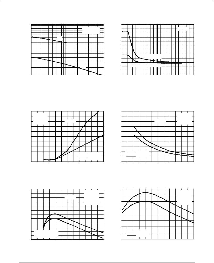
There are two limitations on the power handling ability of a transistor: average junction temperature and second breakdown. Safe operating area curves indicate IC ±VCE limits of the transistor that must be observed for reliable operation; i.e., the transistor must not be subjected to greater dissipation than the curves indicate. The data of Figure 22 is based
on TC = 25°C; TJ(pk) is variable depending on power level. Second breakdown pulse limits are valid for duty cycles to
10% but must be derated when TC > 25°C. Second breakdown limitations do not derate the same as thermal limitations. Allowable current at the voltages shown on Figure 22 may be found at any case temperature by using the appropriate curve on Figure 21.
TJ(pk) may be calculated from the data in Figure 24. At any case temperatures, thermal limitations will reduce the power
that can be handled to values less than the limitations imposed by second breakdown. For inductive loads, high voltage and current must be sustained simultaneously during turn±off with the base to emitter junction reverse biased. The safe level is specified as a reverse biased safe operating area (Figure 23). This rating is verified under clamped conditions so that the device is never subjected to an avalanche mode.
|
100 |
|
|
(AMPS) |
10 |
|
1 μs |
CURRENT |
|
|
|
|
1 ms |
10 μs |
|
1 |
5 ms |
|
|
, COLLECTOR |
|
DC |
EXTENDED |
|
|
||
|
|
SOA |
|
0.1 |
|
|
|
|
|
|
|
C |
|
|
|
I |
|
|
|
|
0.01 |
|
|
|
10 |
100 |
1000 |
VCE, COLLECTOR±EMITTER VOLTAGE (VOLTS)
Figure 22. Forward Bias Safe Operating Area
|
4 |
|
|
|
|
|
|
|
(AMPS) |
|
|
|
|
GAIN ≥ |
4 |
TC ≤ 125°C |
|
|
|
|
|
LC = 500 |
μH |
|||
|
|
|
|
|
|
|||
3 |
|
|
|
|
|
|
|
|
CURRENT |
2 |
|
|
|
|
|
|
|
COLLECTOR |
|
|
|
|
|
|
|
|
1 |
|
|
|
|
|
± 5 V |
|
|
, |
|
|
|
|
|
|
|
|
C |
|
|
|
|
|
|
|
|
I |
|
|
|
|
|
|
|
|
|
0 |
|
|
0 V |
|
±1.5 V |
|
|
|
|
|
|
|
|
|
|
|
|
200 |
300 |
400 |
500 |
600 |
700 |
800 |
900 |
|
|
VCE, COLLECTOR±EMITTER VOLTAGE (VOLTS) |
|
|||||
Figure 23. Reverse Bias Safe Operating Area
TYPICAL THERMAL RESPONSE
|
|
1 |
|
|
|
|
|
|
TRANSIENT THERMAL RESISTANCE |
|
|
0.5 |
|
|
|
|
|
|
|
0.2 |
|
|
|
|
|
|
(NORMALIZED) |
|
0.1 |
|
|
P(pk) |
RθJC(t) = r(t) RθJC |
|
|
0.1 |
0.05 |
|
|
|
||||
|
|
|
RθJC = 2.5°C/W MAX |
|
||||
|
|
|
|
|
|
|||
|
0.02 |
|
|
|
D CURVES APPLY FOR POWER |
|
||
|
|
|
t1 |
PULSE TRAIN SHOWN |
|
|||
|
|
|
|
READ TIME AT t1 |
|
|||
|
SINGLE PULSE |
|
|
t2 |
|
|||
|
|
|
|
DUTY CYCLE, D = t1/t2 |
TJ(pk) ± TC = P(pk) RθJC(t) |
|
||
r(t), |
|
|
|
|
|
|
|
|
|
|
0.01 |
|
|
|
|
|
|
|
|
0.01 |
0.1 |
1 |
10 |
100 |
1000 |
|
t, TIME (ms)
Figure 24. Typical Thermal Response (ZθJC(t)) for BUH51
8 |
Motorola Bipolar Power Transistor Device Data |

BUH51
PACKAGE DIMENSIONS
±B± |
|
||
U |
|
F |
C |
Q |
|
|
M |
|
|
±A± |
|
|
|
|
|
1 |
2 |
3 |
|
H |
|
K |
|
|
|
|
|
V |
J |
G |
R |
S |
0.25 (0.010) M A M B M |
D 2 PL |
|
NOTES:
1.DIMENSIONING AND TOLERANCING PER ANSI Y14.5M, 1982.
2.CONTROLLING DIMENSION: INCH.
|
INCHES |
MILLIMETERS |
||
DIM |
MIN |
MAX |
MIN |
MAX |
A |
0.425 |
0.435 |
10.80 |
11.04 |
B |
0.295 |
0.305 |
7.50 |
7.74 |
C |
0.095 |
0.105 |
2.42 |
2.66 |
D |
0.020 |
0.026 |
0.51 |
0.66 |
F |
0.115 |
0.130 |
2.93 |
3.30 |
G |
0.094 BSC |
2.39 BSC |
||
H |
0.050 |
0.095 |
1.27 |
2.41 |
J |
0.015 |
0.025 |
0.39 |
0.63 |
K |
0.575 |
0.655 |
14.61 |
16.63 |
M |
5 |
TYP |
5 |
TYP |
Q |
0.148 |
0.158 |
3.76 |
4.01 |
R |
0.045 |
0.055 |
1.15 |
1.39 |
S |
0.025 |
0.035 |
0.64 |
0.88 |
U |
0.145 |
0.155 |
3.69 |
3.93 |
V |
0.040 |
±±± |
1.02 |
±±± |
0.25 (0.010) M A M B M |
STYLE 1: |
|
|
PIN 1. |
EMITTER |
|
2. |
COLLECTOR |
|
3. |
BASE |
CASE 77±08
TO±225AA TYPE
ISSUE V
Motorola Bipolar Power Transistor Device Data |
9 |

BUH51
Motorola reserves the right to make changes without further notice to any products herein. Motorola makes no warranty, representation or guarantee regarding the suitability of its products for any particular purpose, nor does Motorola assume any liability arising out of the application or use of any product or circuit, and specifically disclaims any and all liability, including without limitation consequential or incidental damages. ªTypicalº parameters can and do vary in different applications. All operating parameters, including ªTypicalsº must be validated for each customer application by customer's technical experts. Motorola does not convey any license under its patent rights nor the rights of others. Motorola products are not designed, intended, or authorized for use as components in systems intended for surgical implant into the body, or other applications intended to support or sustain life, or for any other application in which the failure of the Motorola product could create a situation where personal injury or death may occur. Should Buyer purchase or use Motorola products for any such unintended or unauthorized application, Buyer shall indemnify and hold Motorola and its officers, employees, subsidiaries, affiliates, and distributors harmless against all claims, costs, damages, and expenses, and reasonable attorney fees arising out of, directly or indirectly, any claim of personal injury or death associated with such unintended or unauthorized use, even if such claim alleges that Motorola was negligent regarding the design or manufacture of the part. Motorola and  are registered trademarks of Motorola, Inc. Motorola, Inc. is an Equal Opportunity/Affirmative Action Employer.
How to reach us: |
|
USA / EUROPE: Motorola Literature Distribution; |
JAPAN: Nippon Motorola Ltd.; Tatsumi±SPD±JLDC, Toshikatsu Otsuki, |
P.O. Box 20912; Phoenix, Arizona 85036. 1±800±441±2447 |
6F Seibu±Butsuryu±Center, 3±14±2 Tatsumi Koto±Ku, Tokyo 135, Japan. 03±3521±8315 |
MFAX: RMFAX0@email.sps.mot.com ± TOUCHTONE (602) 244±6609 HONG KONG: Motorola Semiconductors H.K. Ltd.; 8B Tai Ping Industrial Park, |
|
INTERNET: http://Design±NET.com |
51 Ting Kok Road, Tai Po, N.T., Hong Kong. 852±26629298 |
◊ BUH51/D
*BUH51/D*