

MOTOROLA
SEMICONDUCTOR TECHNICAL DATA
Order this document by MJW21192/D
Complementary Silicon Plastic
Power Transistors
Specifically designed for power audio output, or high power drivers in audio amplifiers.
•DC Current Gain Specified up to 8.0 Amperes at Temperature
•All On Characteristics at Temperature
•High SOA: 20 A, 18 V, 100 ms
•TO±247AE Package
MAXIMUM RATINGS
|
|
MJW21191 |
|
Rating |
Symbol |
MJW21192 |
Unit |
|
|
|
|
Collector±Emitter Voltage |
VCEO |
150 |
Vdc |
Collector±Base Voltage |
VCB |
150 |
Vdc |
Emitter±Base Voltage |
VEB |
5.0 |
Vdc |
Collector Current Ð Continuous |
IC |
8.0 |
Adc |
Ð Peak |
|
16 |
|
|
|
|
|
Base Current |
IB |
2.0 |
Adc |
Total Power Dissipation @ TC = 25_C |
PD |
100 |
Watts |
Derate above 25_C |
|
0.65 |
W/_C |
|
|
|
|
Operating and Storage Junction |
TJ, Tstg |
± 65 to + 150 |
_C |
Temperature Range |
|
|
|
|
|
|
|
THERMAL CHARACTERISTICS
Characteristic |
Symbol |
Max |
Unit |
|
|
|
|
Thermal Resistance, Junction to Case |
RθJC |
0.65 |
_C/W |
Thermal Resistance, Junction to Ambient |
RθJA |
50 |
_C/W |
NPN
MJW21192
PNP
MJW21191
8.0 AMPERES
POWER TRANSISTORS COMPLEMENTARY SILICON
150 VOLTS
100 WATTS
CASE 340K±01 |
TO±247AE |
C, CAPACITANCE (pF)
1000
PNP
NPN
100
10
1.0
1.0 |
10 |
100 |
1000 |
VR, REVERSE VOLTAGE (V)
Figure 1. Typical Capacitance @ 25°C
Motorola, Inc. 1997
Motorola Bipolar Power Transistor Device Data

MJW21192 |
MJW21191 |
|
|
|
|
|
|
ELECTRICAL CHARACTERISTICS (TC = 25_C unless otherwise noted) |
|
|
|
|
|
|
|
|
|
|
|
|
|
|
Characteristic |
Symbol |
Min |
Max |
Unit |
|
|
|
|
|
|
|
|
OFF CHARACTERISTICS |
|
|
|
|
|
|
|
|
|
|
|
|
|
Collector±Emitter Sustaining Voltage (1) |
VCEO(sus) |
|
|
Vdc |
|
|
(IC = 10 mAdc, IB = 0) |
|
150 |
Ð |
|
|
|
Collector Cutoff Current |
ICES |
|
|
μAdc |
|
|
(VCB = 250 Vdc, IE = 0) |
|
Ð |
10 |
|
|
|
Emitter Cutoff Current |
IEBO |
|
|
μAdc |
|
|
(VBE = 5.0 Vdc, IC = 0) |
|
Ð |
10 |
|
|
|
ON CHARACTERISTICS (1) |
|
|
|
|
|
|
|
|
|
|
|
|
|
DC Current Gain |
hFE |
|
|
Ð |
|
|
(IC = 4.0 Adc, VCE = 2.0 Vdc) |
|
15 |
Ð |
100 |
|
|
(IC = 8.0 Adc, VCE = 2.0 Vdc) |
|
5.0 |
Ð |
|
|
|
Collector±Emitter Saturation Voltage |
VCE(sat) |
|
|
Vdc |
|
|
(IC = 4.0 Adc, IB = 0.4 Adc) |
|
Ð |
1.0 |
|
|
|
(IC = 8.0 Adc, IB = 1.6 Adc) |
|
Ð |
2.0 |
|
|
|
Base±Emitter On Voltage |
VBE(on) |
Ð |
2.0 |
Vdc |
|
|
(IC = 4.0 Adc, VCE = 2.0 Vdc) |
|
|
|
|
|
|
DYNAMIC CHARACTERISTICS |
|
|
|
|
|
|
|
|
|
|
|
|
|
Current Gain Ð Bandwidth Product (2) |
fT |
4.0 |
Ð |
MHz |
|
|
(IC = 1.0 Adc, VCE = 10 Vdc, ftest = 1.0 MHz) |
|
|
|
|
|
(1)Pulse Test: Pulse Width v 300 μs, Duty Cycle v 2.0%.
(2)fT = hfe•ftest.
|
|
1.0 |
|
|
|
|
|
|
|
|
DUTY |
|
|
|
D = 0.5 |
|
|
|
|
|
|
|
|
|
|
|
|
|
|
|
|
|
|
CYCLE, |
|
|
RESISTANCE (NORMALIZED) |
|
|
|
|
|
|
|
|
P(pk) |
D = t1/t2 |
TRANSIENT THERMAL |
|
0.2 |
|
|
|
|
|
|
|
|
|
0.1 |
0.1 |
|
|
|
|
|
|
t1 |
|
||
|
|
|
|
|
|
|
t2 |
|
|||
|
0.05 |
|
|
|
|
|
ZθJC(t) = r(t) RθJC |
|
|||
|
|
|
|
|
|
RθJC = 1.65°C/W MAX |
|
||||
|
|
|
|
|
|
|
|
||||
|
|
|
|
|
|
|
D CURVES APPLY FOR POWER |
||||
|
0.02 |
|
|
|
|
|
PULSE TRAIN SHOWN |
|
|||
|
|
|
|
|
|
|
|
|
READ TIME AT t1 |
|
|
|
|
0.01 |
0.01 |
|
|
|
|
|
TJ(pk) ± TC = P(pk) ZθJC(t) |
||
|
|
0.00001 |
0.0001 |
0.001 |
0.01 |
0.1 |
1.0 |
10 |
100 |
1000 |
|
|
|
|
|||||||||
t, TIME (s)
Figure 2. Thermal Response
2 |
Motorola Bipolar Power Transistor Device Data |

There are two limitations on the power handling ability of a transistor: average junction temperature and second breakdown. Safe operating area curves indicate IC ± VCE limits of the transistor that must be observed for reliable operation, i.e., the transistor must not be subjected to greater dissipation then the curves indicate.
MJW21192 MJW21191
The data of Figures 3 and 4 is based on TJ(pk) = 150_C; TC is variable depending on conditions. Second breakdown
pulse limits are valid for duty cycles to 10% provided TJ(pk) < 150_C. TJ(pk) may be calculated from the data in Figure 2. At high case temperatures, thermal limitations will reduce the
power that can be handled to values less than the limitations imposed by second breakdown.
|
|
NPN Ð MJW21192 |
|
|
|
100 |
|
|
|
(AMPS) |
|
|
10 ms |
|
|
100 ms |
|
|
|
CURRENT |
10 |
|
|
|
|
250 ms |
|
|
|
|
|
|
|
|
, COLLECTOR |
1.0 |
|
|
|
|
|
|
|
|
C |
|
|
|
|
I |
|
|
|
|
|
0.1 |
|
|
|
|
1.0 |
10 |
100 |
1000 |
|
|
VCE, COLLECTOR±EMITTER VOLTAGE (VOLTS) |
|
|
Figure 3. NPN Ð MJW21192
Safe Operating Area
|
PNP Ð MJW21191 |
|
(AMPS) |
100 |
|
10 ms |
||
|
||
CURRENT |
100 ms |
|
10 |
||
|
||
COLLECTOR, |
250 ms |
|
1.0 |
||
|
||
C |
|
|
I |
|
|
|
0.1 |
1.0 |
10 |
100 |
1000 |
|
VCE, COLLECTOR±EMITTER VOLTAGE (VOLTS) |
|
|
Figure 4. PNP Ð MJW21191
Safe Operating Area
|
|
|
|
TYPICAL CHARACTERISTICS |
|
|
|
|
|||
|
|
|
NPN Ð MJW21192 |
|
|
|
|
|
PNP Ð MJW21191 |
|
|
|
1000 |
|
|
|
|
|
1000 |
|
|
|
|
|
|
|
|
|
|
|
100°C |
50°C |
|
|
|
|
|
° |
|
|
|
|
|
|
|
|
|
GAIN |
100°C |
50 C |
|
|
|
GAIN |
|
|
|
|
|
|
|
|
|
|
|
|
|
|
|||
100 |
|
|
|
|
100 |
|
|
|
|
||
,DC CURRENT |
|
|
|
|
,DC CURRENT |
|
|
|
|
||
|
|
|
|
|
25°C |
|
|
|
|
||
25°C |
|
|
|
|
|
|
|
|
|
||
10 |
|
|
|
|
10 |
|
|
|
|
||
FE |
|
|
|
|
FE |
|
|
|
|
||
|
|
|
|
|
|
|
|
|
|
||
h |
|
|
|
|
|
h |
|
|
|
|
|
|
1.0 |
0.1 |
|
10 |
100 |
|
1.0 |
0.1 |
|
10 |
|
|
0.01 |
1.0 |
|
0.01 |
1.0 |
100 |
|||||
IC, COLLECTOR CURRENT (AMPS) |
IC, COLLECTOR CURRENT (AMPS) |
Figure 5. NPN Ð MJW21192 |
Figure 6. PNP Ð MJW21191 |
VCE = 2.0 V DC Current Gain |
VCE = 2.0 V DC Current Gain |
Motorola Bipolar Power Transistor Device Data |
3 |

MJW21192 |
MJW21191 |
|
|
|
|||
|
|
|
|
NPN Ð MJW21192 |
|
|
|
|
1000 |
|
|
|
|
|
1000 |
GAIN |
|
|
50°C |
|
|
GAIN |
|
100 |
100°C |
|
|
|
100 |
||
,DC CURRENT |
|
|
|
|
,DC CURRENT |
||
|
25°C |
|
|
|
|
||
10 |
|
|
|
|
10 |
||
FE |
|
|
|
|
FE |
||
|
|
|
|
|
|
||
h |
|
|
|
|
|
h |
|
|
1.0 |
0.01 |
0.1 |
1.0 |
10 |
100 |
1.0 |
|
|
|
|||||
|
|
PNP Ð MJW21191 |
|
|
|
|
50°C |
|
|
100°C |
|
|
|
|
25°C |
|
|
|
|
0.01 |
0.1 |
1.0 |
10 |
100 |
IC, COLLECTOR CURRENT (AMPS) |
I , COLLECTOR CURRENT (AMPS) |
|
C |
Figure 7. NPN Ð MJW21192 |
Figure 8. PNP Ð MJW21191 |
VCE = 5.0 V DC Current Gain |
VCE = 5.0 V DC Current Gain |
|
1.0 |
|
|
(VOLTS) |
|
|
100°C |
|
|
25°C |
|
|
|
|
|
V, VOLTAGE |
0.1 |
|
|
|
|
|
|
|
0.01 |
|
|
|
0.1 |
1.0 |
10 |
IC, COLLECTOR CURRENT (AMPS)
|
|
Figure 9. NPN Ð MJW21192 |
|
|
|
VCE(sat) IC/IB = 5.0 |
|
|
1.0 |
|
|
|
|
|
100°C |
(VOLTS) |
|
|
25°C |
|
|
|
|
V, VOLTAGE |
0.1 |
|
|
|
|
|
|
|
0.01 |
|
|
|
0.1 |
1.0 |
10 |
IC, COLLECTOR CURRENT (AMPS)
Figure 11. NPN Ð MJW21192
VCE(sat) IC/IB = 10
|
1.0 |
|
|
(VOLTS) |
|
|
|
V, VOLTAGE |
0.1 |
|
|
100°C |
|
|
|
|
25°C |
|
|
|
0.01 |
|
|
|
0.1 |
1.0 |
10 |
IC, COLLECTOR CURRENT (AMPS)
|
|
Figure 10. PNP Ð MJW21191 |
|
|
|
VCE(sat) IC/IB = 5.0 |
|
|
10 |
|
|
V,VOLTAGE (VOLTS) |
1.0 |
|
|
0.1 |
|
|
|
|
100°C |
|
|
|
25°C |
|
|
|
0.01 |
|
|
|
0.1 |
1.0 |
10 |
IC, COLLECTOR CURRENT (AMPS)
Figure 12. PNP Ð MJW21191
VCE(sat) IC/IB = 10
4 |
Motorola Bipolar Power Transistor Device Data |

|
|
|
NPN Ð MJW21192 |
|
|
|
10 |
|
|
|
|
(VOLTS) |
|
|
|
|
|
VOLTAGE |
1.0 |
50°C |
|
|
|
25°C |
|
|
|
||
|
|
|
|
||
V, |
|
|
|
|
|
|
100°C |
|
|
|
|
|
0.1 |
0.01 |
0.1 |
|
|
|
0.001 |
1.0 |
10 |
IC, COLLECTOR CURRENT (AMPS)
Figure 13. NPN Ð MJW21192
VCE = 2.0 V VBE(on) Curve
|
|
|
MJW21192 |
MJW21191 |
|
|
|
|
PNP Ð MJW21191 |
|
|
|
10 |
|
|
|
|
(VOLTS) |
|
|
|
|
|
VOLTAGE |
1.0 |
50°C |
|
|
|
25°C |
|
|
|
||
V, |
|
|
|
|
|
|
100°C |
|
|
|
|
|
0.1 |
0.01 |
0.1 |
|
|
|
0.001 |
1.0 |
10 |
||
IC, COLLECTOR CURRENT (AMPS)
Figure 14. PNP Ð MJW21191
VCE = 2.0 V VBE(on) Curve
Motorola Bipolar Power Transistor Device Data |
5 |
MJW21192 MJW21191
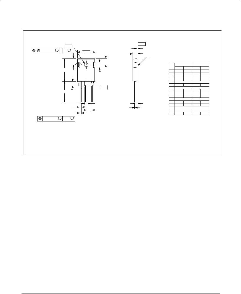
PACKAGE DIMENSIONS
|
±Q± |
|
|
±T± |
|
|
|
|
|
|
|
|
|
E |
|
|
|
|
|
||
0.25 (0.010) M T |
B |
M |
±B± |
|
NOTES: |
|
|
|
|
|
|
C |
|
|
|
|
|||||
|
|
|
|
|
1. DIMENSIONING AND TOLERANCING PER ANSI |
|||||
|
|
|
|
|
4 |
Y14.5M, 1982. |
|
|
|
|
|
|
U |
|
|
L |
2. CONTROLLING DIMENSION: MILLIMETER. |
||||
|
|
|
|
|
|
|
|
|
||
|
|
|
|
|
|
|
MILLIMETERS |
INCHES |
||
|
A |
|
|
|
|
DIM |
MIN |
MAX |
MIN |
MAX |
|
|
|
|
R |
A |
19.7 |
20.3 |
0.776 |
0.799 |
|
|
|
|
|
|
B |
15.3 |
15.9 |
0.602 |
0.626 |
|
|
|
|
|
|
|
|||||
|
|
1 |
2 |
3 |
|
C |
4.7 |
5.3 |
0.185 |
0.209 |
|
|
|
D |
1.0 |
1.4 |
0.039 |
0.055 |
|||
|
|
|
|
|
|
|||||
|
|
|
|
|
|
E |
1.27 REF |
0.050 REF |
||
|
|
|
|
|
±Y± |
F |
2.0 |
2.4 |
0.079 |
0.094 |
|
|
P |
|
|
G |
5.5 BSC |
0.216 BSC |
|||
|
K |
|
|
|
H |
2.2 |
2.6 |
0.087 |
0.102 |
|
|
|
|
|
|
||||||
|
|
|
|
|
J |
0.4 |
0.8 |
0.016 |
0.031 |
|
|
|
|
|
|
|
|||||
|
|
|
|
|
|
K |
14.2 |
14.8 |
0.559 |
0.583 |
|
|
|
|
|
|
L |
5.5 NOM |
0.217 NOM |
||
|
|
|
|
V |
H |
P |
3.7 |
4.3 |
0.146 |
0.169 |
|
|
F |
|
Q |
3.55 |
3.65 |
0.140 |
0.144 |
||
|
|
G |
|
J |
R |
5.0 NOM |
0.197 NOM |
|||
|
|
|
|
|||||||
|
|
D |
|
|
U |
5.5 BSC |
0.217 BSC |
|||
|
|
|
|
|
V |
3.0 |
3.4 |
0.118 |
0.134 |
|
0.25 (0.010) M |
Y |
Q S |
|
|
|
|
|
|
|
|
CASE 340K±03 (TO±247AE)
ISSUE A
6 |
Motorola Bipolar Power Transistor Device Data |

MJW21192 MJW21191
Motorola reserves the right to make changes without further notice to any products herein. Motorola makes no warranty, representation or guarantee regarding the suitability of its products for any particular purpose, nor does Motorola assume any liability arising out of the application or use of any product or circuit, and specifically disclaims any and all liability, including without limitation consequential or incidental damages. ªTypicalº parameters which may be provided in Motorola data sheets and/or specifications can and do vary in different applications and actual performance may vary over time. All operating parameters, including ªTypicalsº must be validated for each customer application by customer's technical experts. Motorola does not convey any license under its patent rights nor the rights of others. Motorola products are not designed, intended, or authorized for use as components in systems intended for surgical implant into the body, or other applications intended to support or sustain life, or for any other application in which the failure of the Motorola product could create a situation where personal injury or death may occur. Should Buyer purchase or use Motorola products for any such unintended or unauthorized application, Buyer shall indemnify and hold Motorola and its officers, employees, subsidiaries, affiliates, and distributors harmless against all claims, costs, damages, and expenses, and reasonable attorney fees arising out of, directly or indirectly, any claim of personal injury or death associated with such unintended or unauthorized use, even if such claim alleges that Motorola was negligent regarding the design or manufacture of the part. Motorola and  are registered trademarks of Motorola, Inc. Motorola, Inc. is an Equal Opportunity/Affirmative Action Employer.
Motorola Bipolar Power Transistor Device Data |
7 |

MJW21192 MJW21191
|
Mfax is a trademark of Motorola, Inc. |
How to reach us: |
|
USA / EUROPE / Locations Not Listed: Motorola Literature Distribution; |
JAPAN: Nippon Motorola Ltd.: SPD, Strategic Planning Office, 4±32±1, |
P.O. Box 5405, Denver, Colorado 80217. 303±675±2140 or 1±800±441±2447 |
Nishi±Gotanda, Shinagawa±ku, Tokyo 141, Japan. 81±3±5487±8488 |
Mfax : RMFAX0@email.sps.mot.com ± TOUCHTONE 602±244±6609 |
ASIA/PACIFIC: Motorola Semiconductors H.K. Ltd.; 8B Tai Ping Industrial Park, |
± US & Canada ONLY 1±800±774±1848 51 Ting Kok Road, Tai Po, N.T., Hong Kong. 852±26629298
INTERNET: http://motorola.com/sps
8 |
◊ |
Motorola Bipolar Power Transistor Device Data |
|
MJW21192/D |