

MOTOROLA
SEMICONDUCTOR TECHNICAL DATA
Order this document by MAC8S/D
Advance Information
TRIACS
Silicon Bidirectional Thyristors
Designed for industrial and consumer applications for full wave control of ac loads such as appliance controls, heater controls, motor controls, and other power switching applications.
•Sensitive Gate Allows Triggering by Microcontrollers and other Logic Circuits
•High Immunity to dv/dt Ð 25 V/ ms Minimum at 110_C
•High Commutating di/dt Ð 8.0 A/ms Minimum at 110 _C
•Minimum and Maximum Values of IGT, VGT and IH Specified for ease of Design
•On-State Current Rating of 8 Amperes RMS at 70_C
•High Surge Current Capability Ð 70 Amperes
•Blocking Voltage to 800 Volts
•Rugged, Economical TO220AB Package
MAXIMUM RATINGS (TJ = 25°C unless otherwise noted)
MAC8S SERIES
TRIACS
8 AMPERES RMS
400 THRU 800
VOLTS
MT2
MT1 
MT2 

G
CASE 221A±06 (TO-220AB)
STYLE 4
Parameter |
|
Symbol |
Value |
Unit |
|
|
|
|
|
Peak Repetitive Off-State Voltage (1) |
|
VDRM |
|
Volts |
(TJ = ±40 to 110°C, Sine Wave, 50 to 60Hz, Gate Open) |
MAC8SD |
|
400 |
|
|
MAC8SM |
|
600 |
|
|
MAC8SN |
|
800 |
|
|
|
|
|
|
On-State RMS Current |
|
IT(RMS) |
8 |
A |
(Full Cycle Sine Wave, 60Hz, TJ = 70°C) |
|
|
|
|
Peak Non-repetitive Surge Current |
|
ITSM |
70 |
A |
(One Half Cycle, 60Hz, TJ = 110°C) |
|
|
|
|
Circuit Fusing Consideration |
|
I2t |
20 |
A2sec |
(t = 8.3 ms) |
|
|
|
|
|
|
|
|
|
Peak Gate Power |
|
PGM |
16 |
Watts |
(Pulse Width ≤ 1.0ms, TC = 70°C) |
|
|
|
|
Average Gate Power |
|
PG(AV) |
0.35 |
Watts |
(t = 8.3ms, TC = 70°C) |
|
|
|
|
Operating Junction Temperature Range |
|
TJ |
± 40 to +110 |
°C |
Storage Temperature Range |
|
Tstg |
± 40 to +150 |
°C |
THERMAL CHARACTERISTICS
Thermal Resistance |
|
|
°C/W |
Ð Junction to Case |
RqJC |
2.2 |
|
Ð Junction to Ambient |
RqJA |
62.5 |
|
Maximum Lead Temperature for Soldering Purposes 1/8″ from Case for 5 Seconds |
TL |
260 |
°C |
(1)VDRM for all types can be applied on a continuous basis. Blocking voltages shall not be tested with a constant current source such that the voltage ratings of the devices are exceeded.
REV 0
Motorola, Inc. 1995

MAC8S |
SERIES |
|
|
|
|
||
ELECTRICAL CHARACTERISTICS (TJ = 25°C unless otherwise noted) |
|
|
|
|
|||
|
|
|
|
|
|
|
|
Characteristic |
|
|
Symbol |
Min |
Typ |
Max |
Unit |
|
|
|
|
|
|
|
|
OFF CHARACTERISTICS |
|
|
|
|
|
|
|
|
|
|
|
|
|
|
|
Peak Repetitive Blocking Current |
TJ = 25°C |
IDRM |
Ð |
Ð |
0.01 |
mA |
|
(VD = Rated VDRM, Gate Open) |
|
|
|||||
|
TJ = 110°C |
|
Ð |
Ð |
2.0 |
|
|
ON CHARACTERISTICS |
|
|
|
|
|
|
|
|
|
|
|
|
|
|
|
Peak On-State Voltage* (ITM = 11A) |
|
|
VTM |
Ð |
Ð |
1.85 |
Volts |
Continuous Gate Trigger Current (VD = 12 V, RL = 100Ω) |
|
|
IGT |
.8 |
2.0 |
5.0 |
mA |
MT2(+), G(+) |
|
|
|
|
|||
MT2(+), G(±) |
|
|
|
.8 |
3.0 |
5.0 |
|
MT2(±), G(±) |
|
|
|
.8 |
3.0 |
5.0 |
|
|
|
|
|
|
|
|
|
Hold Current (VD = 12V, Gate Open, Initiating Current = 150mA) |
|
IH |
1.0 |
3.0 |
10 |
mA |
|
Latching Current (VD = 24V, IG = 5mA) |
|
|
IL |
2.0 |
5.0 |
15 |
mA |
MT2(+), G(+) |
|
|
|
|
|||
MT2(±), G(±) |
|
|
|
2.0 |
10 |
20 |
|
MT2(+), G(±) |
|
|
|
2.0 |
5.0 |
15 |
|
|
|
|
|
|
|
|
|
Gate Trigger Voltage (Continuous dc) (VD = 12 V, RL = 100Ω) |
|
|
VGT |
0.45 |
0.62 |
1.5 |
Volts |
MT2(+), G(+) |
|
|
|
|
|||
MT2(+), G(±) |
|
|
|
0.45 |
0.60 |
1.5 |
|
MT2(±), G(±) |
|
|
|
0.45 |
0.65 |
1.5 |
|
|
|
|
|
|
|
|
|
DYNAMIC CHARACTERISTICS |
|
|
|
|
|
|
|
|
|
|
|
|
|
|
|
Critical Rate of Rise of Off±State Voltage |
|
|
(dv/dt)c |
8.0 |
10 |
Ð |
A/ms |
(VD = 400V, ITM = 3.5A, Commutating dv/dt = 10Vm/sec, |
|
|
|
|
|
|
|
Gate Open, TJ = 110_C, f= 500 Hz, Snubber: CS = 0.01 mF, RS = 15W, |
|
|
|
|
|
||
see Figure 16.) |
|
|
|
|
|
|
|
|
|
|
|
|
|
|
|
Critical Rate of Rise of Off-State Voltage |
|
|
dv/dt |
25 |
75 |
Ð |
V/ms |
(VD = Rate VDRM, Exponential Waveform, RGK = 510W, TJ = 110°C) |
|
|
|
|
|
||
* Indicates Pulse Test: Pulse Width ≤ 2.0 ms, Duty Cycle ≤ 2%. |
|
|
|
|
|
|
|
ALLOWABLE CASE TEMPERATURE C)(° |
110 |
|
|
|
|
|
|
AVERAGE POWER DISSIPATION (WATTS) |
25 |
100 |
|
|
|
|
|
|
20 |
||
|
|
|
|
|
a = 30 and 60° |
|
|||
90 |
|
|
|
|
|
|
15 |
||
|
|
α |
|
|
|
|
|
||
80 |
α |
|
|
|
|
|
10 |
||
|
|
|
|
|
|
||||
|
a = CONDUCTION ANGLE |
|
90° |
|
|
|
|||
70 |
|
|
|
180° |
5 |
||||
|
|
|
|
|
|||||
|
|
|
|
|
|
|
|
||
MAXIMUM |
|
|
|
|
|
|
DC |
, |
|
|
|
|
|
|
|
(AV) |
|
||
60 |
|
|
|
|
|
|
0 |
||
|
|
|
|
|
|
P |
|||
0 |
2 |
4 |
6 |
8 |
10 |
12 |
|
||
, |
|
IT(RMS), RMS ON±STATE CURRENT (AMPS) |
|
|
|
||||
C |
|
|
|
|
|||||
T |
|
|
|
|
|
|
|
|
|
Figure 1.0 RMS Current Derating
|
|
|
|
DC |
|
|
|
|
α |
|
180° |
|
|
|
|
|
120° |
|
|
|
|
α |
|
|
|
|
|
|
|
|
90° |
|
|
|
|
|
|
|
|
|
|
|
a = CONDUCTION ANGLE |
|
° |
|
|
|
|
|
|
|
60 |
|
|
|
|
|
|
|
a = 30° |
|
0 |
2 |
4 |
6 |
8 |
10 |
12 |
|
IT(RMS), RMS ON±STATE CURRENT (AMPS) |
|
|
|||
Figure 2.0 Maximum On±State Power Dissipation
Data Sheets |
2 |
Motorola Thyristor Device Data |

(AMPS)CURRENTON±STATEINSTANTANOUS |
|
|
|
|
|
|
|
|
|
MAC8S |
SERIES |
|
|
|
|
|
|||
100 |
Typical @ TJ = 25 °C |
|
|
|
|
|
|
|
(NORMALIZED)RESISTANCETHERMAL |
1 |
|
|
|
|
|
||||
|
|
|
|
|
|
|
|
|
|
|
|
|
|
||||||
|
|
|
|
|
|
|
|
|
|
|
|
|
|
|
|
||||
|
|
|
|
|
|
|
|
|
Maximum @ |
|
|
|
|
|
|
|
|
|
|
|
|
|
|
|
|
|
|
|
TJ = 110°C |
|
|
|
|
|
ZqJC(t) = RqJC(t) r(t) |
|
|
||
|
10 |
|
|
|
|
|
|
|
|
|
|
|
|
|
|
|
|
||
|
|
|
|
|
|
|
|
|
|
|
|
|
|
|
|
|
|
|
|
|
|
|
|
|
|
|
|
|
|
|
|
|
|
0.1 |
|
|
|
|
|
|
1 |
|
|
|
Maximum @ |
|
|
|
|
|
|
|
|
|
|
|
|
|
|
|
|
|
|
|
|
|
|
|
|
|
|
|
|
|
|
|
|
||
|
|
|
|
|
TJ = 25 °C |
|
|
|
|
|
|
TRANSIENT, |
|
|
|
|
|
|
|
I |
0.5 |
1 |
1.5 |
2 |
2.5 |
3 |
3.5 |
4 |
4.5 |
5 |
5.5 |
6 |
0.1 |
1 |
10 |
100 |
1000 |
1@104 |
|
, |
0.1 |
|
|
|
|
|
|
|
|
|
|
|
|
0.01 |
|
|
|
|
|
T |
|
|
|
|
|
|
|
|
|
|
|
|
|
|
|
|
|
|
|
|
|
|
VT, INSTANTANEOUS ON±STATE VOLTAGE (VOLTS) |
|
|
(t) |
|
|
t, TIME (ms) |
|
|
|
|||||||
|
|
|
|
|
R |
|
|
|
|
|
|||||||||
Figure 3.0 On±State Characteristics |
Figure 4.0 Transient Thermal Response |
|
10 |
|
|
|
|
|
|
|
|
|
|
25 |
|
|
|
|
|
|
|
|
|
|
CURRENTHOLDING(mA) |
8 |
|
|
|
|
|
|
|
|
|
CURRENTLATCHING(mA) |
20 |
|
|
|
|
|
|
|
|
|
|
6 |
|
MT2 POSITIVE |
|
|
|
|
|
15 |
|
|
|
|
|
|
|
|
|
|
||||
|
|
|
|
|
|
|
|
|
|
|
|
|
|
|
|
|
|
|
|
|
||
|
|
|
|
|
|
|
MT2 NEGATIVE |
|
|
|
|
|
|
|
|
|
|
|
|
|
|
|
|
4 |
|
|
|
|
|
|
|
|
|
|
10 |
|
Q3 |
|
|
|
|
|
|
|
|
, |
2 |
|
|
|
|
|
|
|
|
|
, |
5 |
|
|
|
|
|
|
|
|
|
|
H |
|
|
|
|
|
|
|
|
|
L |
|
|
|
|
|
|
|
|
|
|
||
I |
|
|
|
|
|
|
|
|
|
|
I |
|
|
|
|
|
|
|
|
|
|
|
|
|
|
|
|
|
|
|
|
|
|
|
|
Q1 |
|
|
|
|
|
|
|
|
|
|
0 |
±25 |
±10 |
5 |
20 |
35 |
50 |
65 |
80 |
95 |
110 |
0 |
±25 |
±10 |
5 |
20 |
35 |
50 |
65 |
80 |
95 |
110 |
|
±40 |
±40 |
||||||||||||||||||||
|
|
|
|
TJ, JUNCTION TEMPERATURE (°C) |
|
|
|
|
|
|
TJ, JUNCTION TEMPERATURE (°C) |
|
|
|
||||||||
Figure 5.0 Typical Holding Current Versus |
Figure 6.0 Typical Latching Current Versus |
Junction Temperature |
Junction Temperature |
|
14 |
|
|
|
|
|
|
|
|
|
|
(mA) |
12 |
|
|
|
|
|
|
|
|
|
|
|
|
|
|
|
|
|
|
|
|
|
|
CURRENT |
10 |
|
|
|
|
|
|
|
|
|
|
8 |
|
|
|
|
|
|
|
|
|
|
|
TRIGGER |
|
|
|
Q3 |
|
|
|
|
|
|
|
|
|
|
|
|
|
|
|
|
|
||
6 |
|
|
|
|
|
|
|
|
|
|
|
|
|
|
Q2 |
|
|
|
|
|
|
|
|
GATE |
4 |
|
|
|
|
|
|
|
|
|
|
|
|
|
|
|
|
|
|
|
|
||
|
|
|
|
|
|
|
|
|
|
|
|
, |
|
|
|
|
|
|
|
|
|
|
|
GT |
2 |
|
|
|
|
|
|
|
|
|
|
I |
|
Q1 |
|
|
|
|
|
|
|
||
|
|
|
|
|
|
|
|
|
|
||
|
0 |
±25 |
±10 |
5 |
20 |
35 |
50 |
65 |
80 |
95 |
110 |
|
±40 |
||||||||||
|
|
|
|
TJ, JUNCTION TEMPERATURE (°C) |
|
|
|
||||
Figure 7.0 Typical Gate Trigger Current Versus
Junction Temperature
|
1 |
|
|
|
|
|
|
|
|
|
|
(VOLTS) |
0.9 |
|
Q1 |
|
|
|
|
|
|
|
|
|
|
|
|
|
|
|
|
|
|
||
|
Q3 |
|
|
|
|
|
|
|
|
|
|
VOLTAGE |
0.8 |
|
|
|
|
|
|
|
|
|
|
|
|
|
|
|
|
|
|
|
|
||
0.7 |
|
|
|
|
|
|
|
|
|
|
|
TRIGGER |
0.6 |
|
|
|
|
|
|
|
|
|
Q3 |
|
|
|
|
|
|
|
|
|
|
|
|
GATE |
0.5 |
|
|
|
|
Q2 |
|
|
|
|
|
|
|
|
|
|
|
|
|
|
|
|
|
, |
0.4 |
|
|
|
|
|
|
|
Q1 |
|
|
GT |
|
|
|
|
|
|
|
|
|
||
|
|
|
|
|
|
|
|
|
|
|
|
V |
|
|
|
|
|
|
|
|
|
|
|
|
0.3 |
±25 |
±10 |
5 |
20 |
35 |
50 |
65 |
80 |
95 |
110 |
|
±40 |
||||||||||
|
|
|
TJ, JUNCTION TEMPERATURE (°C) |
|
|
|
|||||
Figure 8.0 Typical Gate Trigger Voltage Versus
Junction Temperature
Motorola Thyristor Device Data |
3 |
Data Sheets |
|
|
|
|
|
|
|
|
|
MAC8S |
SERIES |
|
|
|
|
|
|
|
|
|
200 |
|
|
|
|
|
|
|
|
|
|
130 |
|
|
|
|
|
|
|
|
180 |
|
|
|
|
|
|
|
TJ = 110°C |
|
|
|
|
|
|
RG ± MT1 = 510W |
|
|||
|
|
|
|
|
|
|
|
|
|
120 |
|
|
|
|
|
|
|
|
|
|
|
|
|
|
|
|
|
|
|
|
|
|
|
|
TJ = 100°C |
|
|
|
|
160 |
V |
PK |
= 400V |
|
|
|
|
|
|
|
|
|
|
|
|
|
|
|
|
STATICdv/dt (V/mS) |
|
|
|
|
|
|
|
|
|
|
110 |
|
|
|
|
|
|
|
|
|
|
|
|
|
|
|
|
|
|
STATICdv/dt (V/S)m |
|
|
|
|
|
|
|
|
|
140 |
|
|
|
|
600V |
|
|
|
|
|
|
|
|
|
|
|
|
|
|
120 |
800V |
|
|
|
|
|
|
|
|
|
|
|
|
|
|
110°C |
|
|
|
|
|
|
|
|
|
|
|
|
|
100 |
|
|
|
|
|
|
|
||
|
|
|
|
|
|
|
|
|
|
|
|
|
|
|
|
|
|
||
|
|
|
|
|
|
|
|
|
|
|
|
|
|
|
|
|
|
|
|
100 |
|
|
|
|
|
|
|
|
|
|
|
|
|
|
|
|
|
|
|
|
|
|
|
|
|
|
|
|
|
|
90 |
|
|
|
|
|
120°C |
|
|
80 |
|
|
|
|
|
|
|
|
|
|
|
|
|
|
|
|
|
|
|
|
|
|
|
|
|
|
|
|
|
|
|
|
|
|
|
|
|
|
|
60 |
|
|
|
|
|
|
|
|
|
|
80 |
|
|
|
|
|
|
|
|
100 |
200 |
|
300 |
400 |
500 |
600 |
700 |
800 |
900 |
1000 |
400 |
450 |
500 |
550 |
600 |
650 |
700 |
750 |
800 |
|
|
|
RGK, GATE±MT1 RESISTANCE (OHMS) |
|
|
|
|
|
VPK, Peak Voltage (Volts) |
|
|
|
|||||||
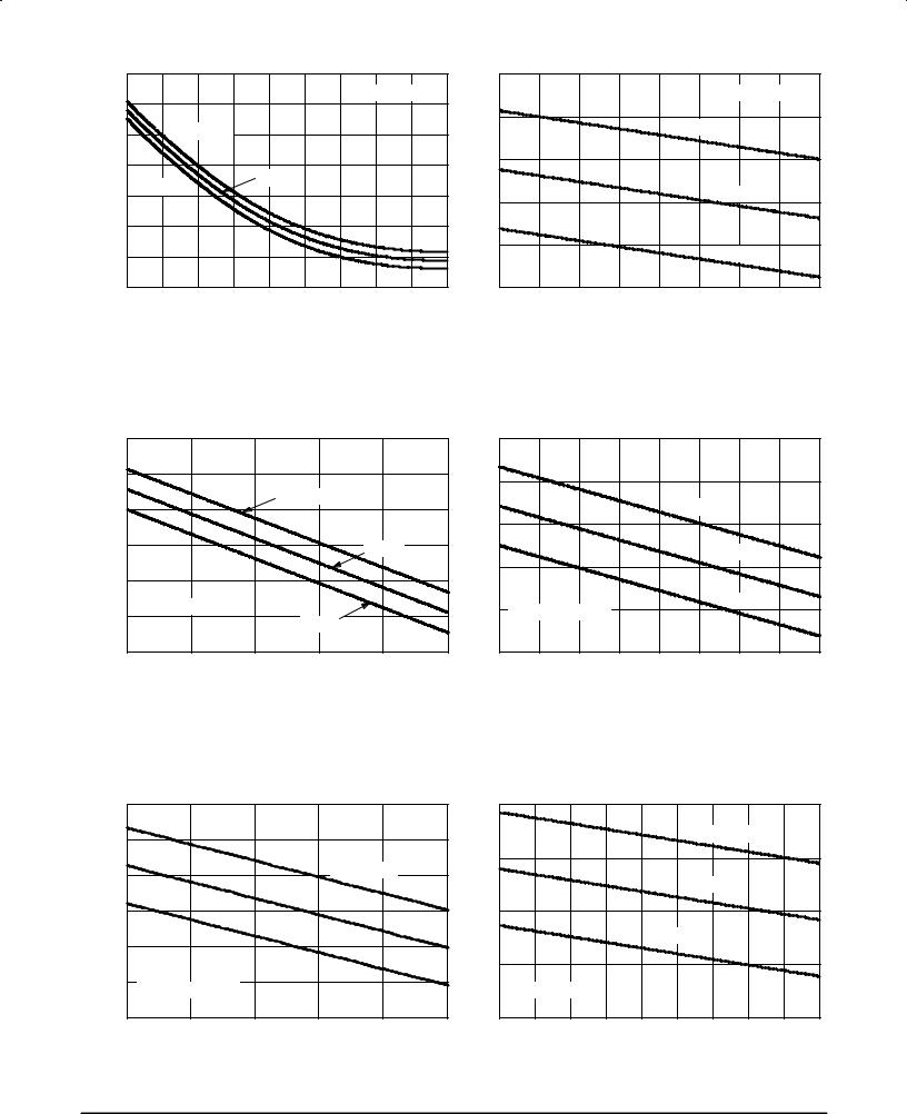
Figure 9.0 Typical Exponential Static dv/dt Versus |
Figure 10.0 Typical Exponential Static dv/dt Versus |
Gate±MT1 Resistance, MT2(+) |
Peak Voltage, MT2(+) |
|
130 |
|
|
|
|
|
350 |
|
|
|
|
|
|
|
|
|
120 |
|
|
|
|
|
300 |
|
|
|
|
|
|
|
|
|
|
|
|
|
|
|
|
|
|
|
|
|
|
|
|
dv/dtSTATIC(V/mS) |
110 |
|
|
VPK = 400V |
|
|
|
|
|
|
TJ = 100°C |
|
|
|
|
|
|
|
|
|
|
|
|
|
|
|
|
||||
|
|
|
|
|
|
250 |
|
|
|
|
|
|
|
|
|
100 |
|
|
|
600V |
|
dv/dtSTATIC(V/S)m |
|
|
|
|
110°C |
|
|
||
|
|
|
|
|
|
|
|
|
|
|
|
||||
|
|
|
|
|
|
|
|
|
|
|
|
|
|||
|
90 |
|
|
|
|
|
200 |
|
|
|
|
|
|
|
|
|
|
|
|
|
|
|
|
|
|
|
|
|
|
|
|
|
|
RG ± MT1 = 510W |
|
|
|
150 |
|
|
W |
|
|
120°C |
|
|
|
|
80 |
|
|
|
|
|
|
|
|
|
|
||||
|
|
|
800V |
|
|
|
RG ± MT1 = 510 |
|
|
|
|
|
|||
|
|
|
|
|
|
|
|
|
|
|
|
|
|
|
|
|
70100 |
105 |
110 |
115 |
120 |
125 |
100 |
|
|
|
|
|
|
|
|
|
400 |
450 |
500 |
550 |
600 |
650 |
700 |
750 |
800 |
||||||
|
|
|
TJ, Junction Temperature (°C) |
|
|
|
|
|
VPK, Peak Voltage |
(Volts) |
|
|
|
||
Figure 11.0 Typical Exponential Static dv/dt Versus |
Figure 12.0 Typical Exponential Static dv/dt Versus |
Junction Temperature, MT2(+) |
Peak Voltage, MT2(±) |
|
350 |
|
|
|
|
|
|
300 |
|
|
|
|
|
|
|
|
|
|
300 |
|
|
|
|
|
|
|
|
|
|
|
|
VPK = 400V |
|
|
|
|
|
|
|
|
|
|
|
|
|
|
|
|
|
|
|
|
|
|
|
|
|
|
VPK = 400V |
|
|
250 |
|
|
|
|
|
|
|
|
|
S) |
250 |
|
|
|
|
S) |
|
|
|
|
|
|
600V |
|
|
|
|
(V/m |
|
|
|
|
|
(V/m |
|
|
|
|
|
|
|
|
|
||
|
|
|
600V |
|
|
|
|
|
|
|
|
|
|
|
|||
|
|
|
|
|
|
|
|
|
|
|
|
|
|
|
|||
dv/dt |
200 |
|
|
|
|
|
dv/dt |
200 |
|
|
|
|
|
|
|
|
|
|
|
|
|
|
|
|
|
|
|
|
|
|
|
|
|
||
STATIC |
|
|
|
800V |
|
|
STATIC |
|
|
|
|
|
800V |
|
|
|
|
150 |
|
|
|
|
|
|
|
|
|
|
|
|
|
|
|
||
|
|
|
|
|
|
150 |
|
|
|
|
|
|
|
|
|
||
|
|
|
|
|
|
|
|
|
|
|
|
|
|
|
|
|
|
|
100 |
RG ± MT1 = 510W |
|
|
|
|
|
TJ = 110°C |
|
|
|
|
|
|
|
||
|
|
|
|
|
|
|
|
|
|
|
|
|
|
||||
|
50 |
105 |
110 |
115 |
120 |
125 |
|
100 |
200 |
300 |
400 |
500 |
600 |
700 |
800 |
900 |
1000 |
|
100 |
|
100 |
||||||||||||||
|
|
|
TJ, Junction Temperature (°C) |
|
|
|
|
|
RGK, GATE±MT1 RESISTANCE (OHMS) |
|
|
||||||
Figure 13.0 Typical Exponential Static dv/dt Versus |
Figure 14.0 Typical Exponential Static dv/dt Versus |
Junction Temperature, MT2(±) |
Gate±MT1 Resistance, MT2(±) |
Data Sheets |
4 |
Motorola Thyristor Device Data |

MAC8S SERIES
s) |
|
|
|
|
|
|
|
|
m |
|
|
|
|
|
|
|
|
(V/ |
|
|
|
|
|
|
|
|
VOLTAGE |
100 |
|
|
|
|
|
|
|
|
|
|
VPK = 400V |
|
|
|
||
COMMUTATING |
|
|
|
|
|
|
||
|
|
|
|
|
90°C |
|
||
10 |
|
|
|
|
|
|
||
OF |
|
|
|
|
100°C |
|
||
|
|
|
|
|
|
|||
RISE |
|
|
1 |
|
|
|
|
|
OF |
|
f = |
|
|
|
|
||
|
2 tw |
|
|
|
|
|||
RATE |
|
tw |
6f ITM |
110°C |
|
|
|
|
|
|
|
|
|
||||
|
(di/dt)c = 1000 |
|
|
|
||||
, CRITICAL |
|
VDRM |
|
|
|
|
|
|
1 |
5 |
10 |
15 |
20 |
25 |
30 |
||
1 |
||||||||
(di/dt)c, CRITICAL RATE OF CHANGE OF COMMUTATING CURRENT (A/ms) |
||||||||
c |
||||||||
(dv/dt) |
Figure 15.0 |
Critical Rate of Rise of |
|
|
||||
|
|
Commutating Voltage |
|
|
||||
|
|
|
|
|
||||
|
|
|
|
|
|
|
|
|
|
|
|
|
|
|
|
|
|
|
|
|
|
|
|
|
|
|
|
|
|
|
|
|
|
|
|
|
|
|
|
|
|
|
|
|
|
|
|
|
|
|
|
|
|
|
|
|
|
|
|
|
|
|
|
|
|
20 mHY |
|
|
|
|
|
|
|
1N4007 |
|
|
|
|
|
|
|||
400 V |
|
|
|
|
|
|
|
|
|
|
LL |
|
|
|
|
|
|
|
|
|
|
|
|
|
|
|
|
RMS |
|
|
|
|
|
|
|
|
|
|
|
|
|
|
|
|
|
|
|
|
|
|
|
|
|
|
|
ADJUST FOR |
|
|
|
|
|
|
|
|
|
|
|
MEASURE |
|
|
15W |
|
|
|
|
|
|
||||||
ITM, 60 Hz VAC |
|
|
|
|
|
|
|
|
|
|
|
|
I |
|
|
|
RS |
|
|
|
|
|
|
||||
|
|
|
|
|
|
|
|
CONTROL |
|
|
|
|
|
|
|
|
|
|
|
|
|
||||||
|
|
|
TRIGGER |
CHARGE |
|
|
|
|
|
|
|
|
|
|
|
|
|
|
|
± |
|
|
|
|
|
||
|
|
|
|
|
|
|
|
|
|
|
|
|
|
|
|
|
|
|
|
|
|
|
|
||||
CHARGE |
CONTROL |
|
|
|
|
|
|
|
|
|
|
CS |
|
|
0.01 mF |
|
|
|
|
400 V |
|||||||
|
|
|
|
|
|
|
|
|
|
|
|
|
+ |
|
|
|
|
||||||||||
|
|
|
|
|
|
|
|
|
|
|
|
|
|
|
|
|
|
|
|||||||||
|
|
|
|
|
|
|
|
|
|
TRIGGER |
|
|
|
2 |
|
|
ADJUST FOR |
|
|
|
|
|
|||||
|
|
|
|
|
|
|
|
|
|
|
|
|
|
|
|
|
|
|
|
||||||||
|
|
|
|
|
|
|
|
|
|
|
|
|
|
|
|
|
|
|
|
|
|
|
|||||
|
|
|
|
NON-POLAR |
|
|
1N914 |
G |
1 |
|
|
|
|
dv/dt(c) |
|
|
|
|
|
|
|||||||
|
|
|
|
|
5 mF |
|
|
|
|
|
|
|
|
|
|
|
|
|
|
|
|
|
|
|
|
||
|
|
|
|
|
|
|
|
|
|
|
|
|
|
|
|
|
|
|
|
|
|
|
|
|
|
|
|
|
|
|
|
|
|
|
|
|
|
|
|
|
|
|
|
|
|
|
|
|
|
|
|
|
|
|
|
|
|
|
|
|
CL |
|
|
|
|
|
|
|
|
|
|
|
|
|
|
|
|
|
|
|
|
||
|
|
|
|
|
|
|
|
|
|
|
|
|
|
|
|
|
|
|
|
|
|
||||||
|
|
|
|
|
|
|
|
|
|
|
|
|
|
|
|
|
|
|
|
|
|
|
|
|
|
||
|
|
|
Note: Component values are for verification of rated (dv/dt)c. See AN1048 for additional information. |
|
|
|
|
|
|
||||||||||||||||||
Figure 16.0 Simplified Test Circuit to Measure the Critical Rate of Rise of Commutating Voltage
Motorola Thyristor Device Data |
5 |
Data Sheets |

MAC8S SERIES
NOTES
Data Sheets |
6 |
Motorola Thyristor Device Data |

MAC8S SERIES
NOTES
Motorola Thyristor Device Data |
7 |
Data Sheets |

|
|
|
|
MAC8S |
SERIES |
|
|
|
|
|
|
|
|
|
|
PACKAGE DIMENSIONS |
|
|
|
|
|
||
|
|
|
|
±T± PLANESEATING |
|
NOTES: |
|
|
|
|
|
|
|
|
|
|
1. DIMENSIONING AND TOLERANCING PER ANSI |
||||||
|
|
|
|
C |
|
|
Y14.5M, 1982. |
|
|
|
|
|
B |
F |
|
|
2. |
CONTROLLING DIMENSION: INCH. |
|
||||
|
|
|
T |
S |
|
3. DIMENSION Z DEFINES A ZONE WHERE ALL |
|||||
|
|
|
|
|
BODY AND LEAD IRREGULARITIES ARE |
||||||
4 |
|
|
|
|
|
|
ALLOWED. |
|
|
|
|
|
|
|
|
|
|
|
|
|
|
|
|
|
|
|
|
|
|
|
|
INCHES |
MILLIMETERS |
||
Q |
|
A |
|
|
|
|
DIM |
MIN |
MAX |
MIN |
MAX |
|
|
|
|
|
A |
0.570 |
0.620 |
14.48 |
15.75 |
||
|
|
|
|
|
|
|
|||||
1 |
2 |
3 |
U |
|
|
|
B |
0.380 |
0.405 |
9.66 |
10.28 |
|
|
|
C |
0.160 |
0.190 |
4.07 |
4.82 |
||||
H |
|
|
|
|
|
|
|||||
|
|
|
|
|
|
D |
0.025 |
0.035 |
0.64 |
0.88 |
|
|
|
K |
|
|
STYLE 4: |
|
F |
0.142 |
0.147 |
3.61 |
3.73 |
|
|
|
|
|
G |
0.095 |
0.105 |
2.42 |
2.66 |
||
Z |
|
|
|
|
PIN 1. |
MAIN TERMINAL 1 |
H |
0.110 |
0.155 |
2.80 |
3.93 |
|
|
|
|
|
2. |
MAIN TERMINAL 2 |
J |
0.018 |
0.025 |
0.46 |
0.64 |
|
|
|
|
|
3. |
GATE |
|||||
|
|
|
|
|
K |
0.500 |
0.562 |
12.70 |
14.27 |
||
|
|
|
|
|
4. |
MAIN TERMINAL 2 |
|||||
L |
|
|
|
R |
L |
0.045 |
0.060 |
1.15 |
1.52 |
||
|
|
|
|
|
|||||||
|
|
|
|
|
N |
0.190 |
0.210 |
4.83 |
5.33 |
||
|
|
|
|
|
|
|
|||||
V |
|
|
|
J |
|
|
Q |
0.100 |
0.120 |
2.54 |
3.04 |
G |
|
|
|
|
|
|
R |
0.080 |
0.110 |
2.04 |
2.79 |
|
|
|
|
|
|
S |
0.045 |
0.055 |
1.15 |
1.39 |
|
|
|
D |
|
|
|
|
T |
0.235 |
0.255 |
5.97 |
6.47 |
|
|
|
CASE 221A±06 |
|
U |
0.000 |
0.050 |
0.00 |
1.27 |
||
|
N |
|
|
|
|||||||
|
|
|
|
V |
0.045 |
±±± |
1.15 |
±±± |
|||
|
|
|
|
(TO-220AB) |
|
Z |
±±± |
0.080 |
±±± |
2.04 |
|
|
|
|
|
|
|
|
|
|
|
||
Motorola reserves the right to make changes without further notice to any products herein. Motorola makes no warranty, representation or guarantee regarding the suitability of its products for any particular purpose, nor does Motorola assume any liability arising out of the application or use of any product or circuit, and specifically disclaims any and all liability, including without limitation consequential or incidental damages. ªTypicalº parameters can and do vary in different applications. All operating parameters, including ªTypicalsº must be validated for each customer application by customer's technical experts. Motorola does not convey any license under its patent rights nor the rights of others. Motorola products are not designed, intended, or authorized for use as components in systems intended for surgical implant into the body, or other applications intended to support or sustain life, or for any other application in which the failure of the Motorola product could create a situation where personal injury or death may occur. Should Buyer purchase or use Motorola products for any such unintended or unauthorized application, Buyer shall indemnify and hold Motorola and its officers, employees, subsidiaries, affiliates, and distributors harmless against all claims, costs, damages, and expenses, and reasonable attorney fees arising out of, directly or indirectly, any claim of personal injury or death associated with such unintended or unauthorized use, even if such claim alleges that Motorola was negligent regarding the design or manufacture of the part. Motorola and  are registered trademarks of Motorola, Inc. Motorola, Inc. is an Equal Opportunity/Affirmative Action Employer.
To order literature by mail:
USA/EUROPE: Motorola Literature Distribution; P.O. Box 20912; Phoenix, Arizona 85036.
JAPAN: Nippon Motorola Ltd.; 4±32±1, Nishi±Gotanda, Shinagawa±ku, Tokyo 141, Japan.
ASIA PACIFIC: Motorola Semiconductors H.K. Ltd.; Silicon Harbour Center, No. 2 Dai King Street, Tai Po Industrial Estate, Tai Po, N.T., Hong Kong.
To order literature electronically:
MFAX: RMFAX0@email.sps.mot.com ±TOUCHTONE (602) 244±6609 INTERNET: http://Design±NET.com
|
|
|
|
|
◊ |
MAC8S/D |
|
*MAC8S/D*