

MOTOROLA
SEMICONDUCTOR TECHNICAL DATA
Order this document by 2N6504/D
Thyristors
Silicon Controlled Rectifiers
. . . designed primarily for half-wave ac control applications, such as motor controls, heating controls and power supply crowbar circuits.
•Glass Passivated Junctions with Center Gate Fire for Greater Parameter Uniformity and Stability
•Small, Rugged, Thermowatt Constructed for Low Thermal Resistance, High Heat Dissipation and Durability
•Blocking Voltage to 800 Volts
•300 A Surge Current Capability
MAXIMUM RATINGS (TJ = 25°C unless otherwise noted.)
2N6504 thru 2N6509*
*Motorola preferred devices
SCRs
25 AMPERES RMS
50 thru 800 VOLTS
G
A 

 K
K
CASE 221A-04 (TO-220AB)
STYLE 3
|
Rating |
|
Symbol |
Value |
Unit |
|
|
|
|
|
|
|
|
* Peak Forward and Reverse Blocking Voltage(1) |
V |
DRM |
, V |
|
Volts |
|
(Gate Open, TJ = 25 to 125°C) |
2N6504 |
|
RRM |
50 |
|
|
|
|
|
|
|||
|
2N6505 |
|
|
|
100 |
|
|
2N6506 |
|
|
|
200 |
|
|
2N6507 |
|
|
|
400 |
|
|
2N6508 |
|
|
|
600 |
|
|
2N6509 |
|
|
|
800 |
|
|
|
|
|
|
|
|
Forward Current (TC = 85°C) |
|
|
IT(RMS) |
25 |
Amps |
|
(180° Conduction Angle) |
|
|
IT(AV) |
16 |
|
|
Peak Non-repetitive Surge Current Ð |
8.3 ms |
|
ITSM |
300 |
Amps |
|
(1/2 Cycle, Sine Wave) |
1.5 ms |
|
|
|
350 |
|
|
|
|
|
|
|
|
Forward Peak Gate Power |
|
|
PGM |
20 |
Watts |
|
Forward Average Gate Power |
|
|
PG(AV) |
0.5 |
Watt |
|
Forward Peak Gate Current |
|
|
IGM |
2 |
Amps |
|
Operating Junction Temperature Range |
|
TJ |
±40 to +125 |
°C |
||
Storage Temperature Range |
|
|
Tstg |
±40 to +150 |
°C |
|
*THERMAL CHARACTERISTICS |
|
|
|
|
|
|
|
|
|
|
|
||
Characteristic |
|
Symbol |
Max |
Unit |
||
|
|
|
|
|
|
|
Thermal Resistance, Junction to Case |
|
|
RθJC |
1.5 |
°C/W |
|
*Indicates JEDEC Registered Data. |
|
|
|
|
|
|
1.VDRM and VRRM for all types can be applied on a continuous basis. Ratings apply for zero or negative gate voltage; however, positive gate voltage shall not be applied concurrent with negative potential on the anode. Blocking voltages shall not be tested with a constant current
source such that the voltage ratings of the devices are exceeded.
Preferred devices are Motorola recommended choices for future use and best overall value.
REV 1
Motorola, Inc. 1995
2N6504 thru 2N6509
ELECTRICAL CHARACTERISTICS (TC = 25°C unless otherwise noted.)
Characteristic |
|
Symbol |
Min |
Typ |
Max |
Unit |
|
|
|
|
|
|
|
* Peak Forward or Reverse Blocking Current |
TJ = 25°C |
IDRM, IRRM |
Ð |
Ð |
10 |
μA |
(VAK = Rated VDRM or VRRM, Gate Open) |
|
|||||
|
TJ = 125°C |
|
Ð |
Ð |
2 |
mA |
(1) |
|
VTM |
Ð |
Ð |
1.8 |
Volts |
* Forward ªOnº Voltage |
|
|||||
(ITM = 50 A) |
|
|
|
|
|
|
* Gate Trigger Current (Continuous dc) |
TC = 25°C |
IGT |
Ð |
Ð |
40 |
mA |
(Anode Voltage = 12 Vdc, RL = 100 Ohms) |
TC = ±40°C |
|
Ð |
25 |
75 |
|
* Gate Trigger Voltage (Continuous dc) |
|
VGT |
Ð |
1 |
1.5 |
Volts |
(Anode Voltage = 12 Vdc, RL = 100 Ohms, TC = ±40°C) |
|
|
|
|
|
|
Gate Non-Trigger Voltage |
|
VGD |
0.2 |
Ð |
Ð |
Volts |
(Anode Voltage = Rated VDRM, RL = 100 Ohms, TJ = 125°C) |
|
|
|
|
|
|
* Holding Current |
|
IH |
Ð |
35 |
40 |
mA |
(Anode Voltage = 12 Vdc, TC = ±40°C) |
|
|
|
|
|
|
* Turn-On Time |
|
tgt |
Ð |
1.5 |
2 |
μs |
(ITM = 25 A, IGT = 50 mAdc) |
|
|
|
|
|
|
Turn-Off Time (VDRM = rated voltage) |
|
tq |
Ð |
15 |
Ð |
μs |
(ITM = 25 A, IR = 25 A) |
|
|
|
|||
(ITM = 25 A, IR = 25 A, TJ = 125°C) |
|
|
Ð |
35 |
Ð |
|
Critical Rate of Rise of Off-State Voltage |
|
dv/dt |
Ð |
50 |
Ð |
V/μs |
(Gate Open, Rated VDRM, Exponential Waveform) |
|
|
|
|
|
|
*Indicates JEDEC Registered Data. |
|
|
|
|
|
|
1. Pulse Test: Pulse Width p 300 μs, Duty Cycle p 2%. |
|
|
|
|
|
|
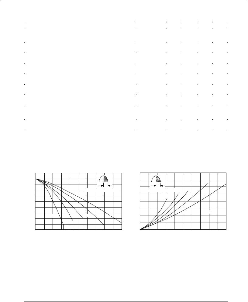
FIGURE 1 Ð AVERAGE CURRENT DERATING
°C) |
130 |
|
|
|
|
|
( |
|
|
|
|
|
|
TEMPERATURE |
110 |
|
|
|
|
|
|
120 |
|
|
|
α |
|
|
|
|
|
α = CONDUCTION ANGLE |
||
CASE |
90 |
|
|
|
|
|
MAXIMUM, |
|
|
|
|
|
|
|
100 |
|
|
|
|
|
|
|
α = 30° |
60° |
90° |
180° |
dc |
C |
|
|
|
|
|
|
T |
|
|
|
|
|
|
|
80 |
|
|
|
|
|
|
0 |
4.0 |
8.0 |
12 |
16 |
20 |
IT(AV), ON-STATE FORWARD CURRENT (AMPS)
FIGURE 2 Ð MAXIMUM ON-STATE POWER DISSIPATION
(WATTS) |
32 |
|
|
|
|
|
|
24 |
α |
|
|
|
180° |
|
|
|
|
|
|
|
|
||
|
|
|
|
|
|
|
|
POWER |
|
α = CONDUCTION ANGLE |
60° |
90° |
|
dc |
|
|
|
|
|||||
|
|
|
|
||||
AVERAGE, |
|
|
α = 30° |
|
|
TJ = 125°C |
|
16 |
|
|
|
|
|
||
|
|
|
|
|
|
|
|
(AV) |
8.0 |
|
|
|
|
|
|
|
|
|
|
|
|
|
|
P |
|
|
|
|
|
|
|
|
0 |
|
|
|
|
|
|
|
0 |
4.0 |
8.0 |
|
12 |
16 |
20 |
|
|
IT(AV), AVERAGE ON-STATE FORWARD CURRENT (AMPS) |
|
||||
2 |
Motorola Thyristor Device Data |
2N6504 thru 2N6509
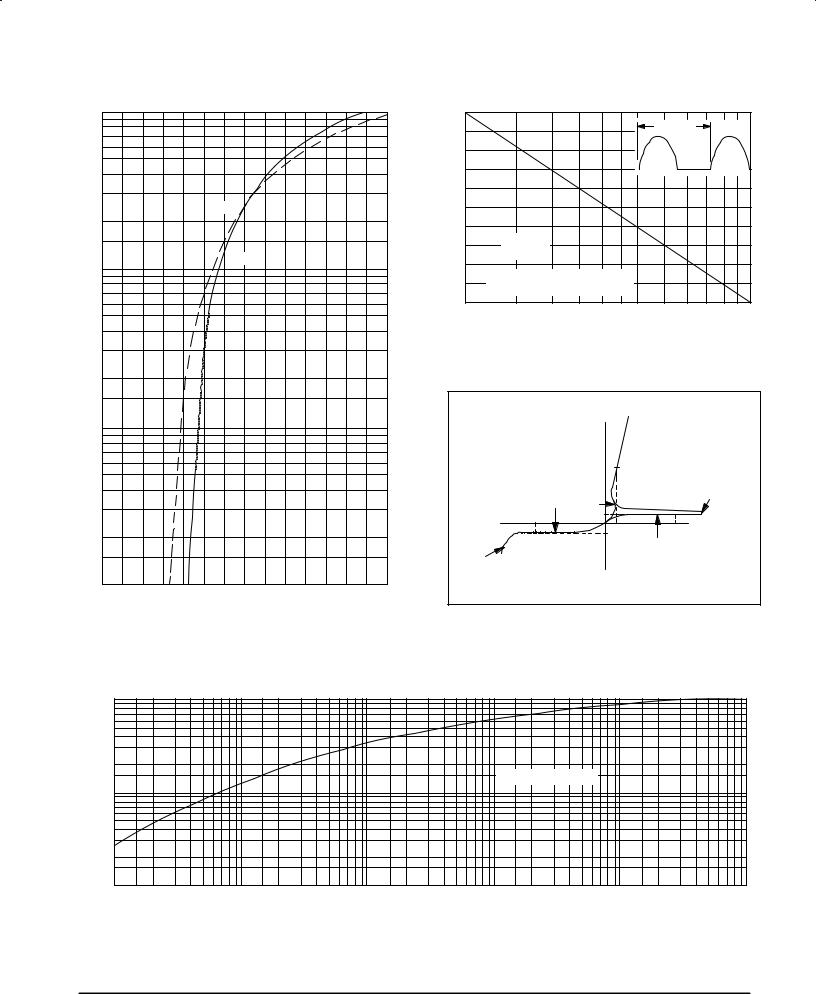
FIGURE 3 Ð MAXIMUM FORWARD VOLTAGE |
FIGURE 4 Ð MAXIMUM NON-REPETITIVE SURGE CURRENT |
100
70
50
30
20
(AMPS) |
10 |
|
CURRENT |
||
7.0 |
||
|
||
FORWARD |
5.0 |
|
3.0 |
||
INSTANTANEOUS |
||
1.0 |
||
|
2.0 |
|
, |
|
|
F |
|
|
i |
0.7 |
|
|
||
|
0.5 |
0.3
0.2
0.1
0
|
|
300 |
|
|
|
|
|
|
|
(AMP) |
|
|
|
|
1 CYCLE |
|
|
|
275 |
|
|
|
|
|
|
|
|
CURRENT |
250 |
|
|
|
|
|
|
125°C |
SURGE |
225 |
|
|
|
|
|
|
25°C |
PEAK, |
|
f = 60 Hz |
|
|
|
|
|
|
|
|
TC = 85°C |
|
|
|
|
|
|
TSM |
200 |
|
|
|
|
|
|
|
|
SURGE IS PRECEDED AND |
|
|
|
|
||
|
|
|
|
|
|
|
||
|
I |
|
FOLLOWED BY RATED CURRENT |
|
|
|
|
|
|
|
175 |
|
|
|
|
||
|
|
2.0 |
3.0 |
4.0 |
6.0 |
8.0 |
10 |
|
|
|
1.0 |
||||||
|
|
|
|
NUMBER OF CYCLES |
|
|
|
|
FIGURE 5 Ð CHARACTERISTICS AND SYMBOLS
|
|
|
|
|
|
|
|
+I |
|
|
|
|
|
|
|
|
|
REVERSE |
IT |
|
FORWARD |
|
|
|
|
|
|
|
|
|
BREAKOVER |
|
|
|
|
|
|
|
|
BLOCKING |
|
VT |
POINT |
|
|
|
|
|
|
|
REGION |
IH |
|
|
|
|
|
|
|
|
|
|
|
||
|
|
|
|
|
|
|
±V |
IDRM |
|
+V |
|
|
|
|
|
|
|
VRRM |
I |
RRM |
VDRM |
|
|
|
|
|
|
|
|
|
||
|
|
|
|
|
|
|
|
|
FORWARD |
|
|
|
|
|
|
|
|
|
|
|
|
|
|
|
|
|
|
|
REVERSE |
|
|
BLOCKING |
|
|
|
|
|
|
|
±I |
|
REGION |
|
|
|
|
|
|
|
|
AVALANCHE |
|
||
|
|
|
|
|
|
|
|
|
||
0.4 |
0.8 |
1.2 |
1.6 |
2.0 |
2.4 |
2.8 |
REGION |
|
|
|
|
vF, INSTANTANEOUS VOLTAGE (VOLTS) |
|
|
|
|
|
|
|||
TRANSIENT THERMAL RESISTANCE |
(NORMALIZED) |
r(t), |
|
FIGURE 6 Ð THERMAL RESPONSE
1.0
0.7
0.5
0.3
0.2
ZθJC(t) = RθJC •r(t)
0.1
0.07
0.05
0.03
0.02
0.01
0.1 |
0.2 0.3 |
0.5 |
1.0 |
2.0 3.0 |
5.0 |
10 |
20 30 |
50 |
100 |
200 300 500 |
1.0 k |
2.0 k 3.0 k 5.0 k |
10 k |
t, TIME (ms)
Motorola Thyristor Device Data |
3 |
2N6504 thru 2N6509
TYPICAL TRIGGER CHARACTERISTICS
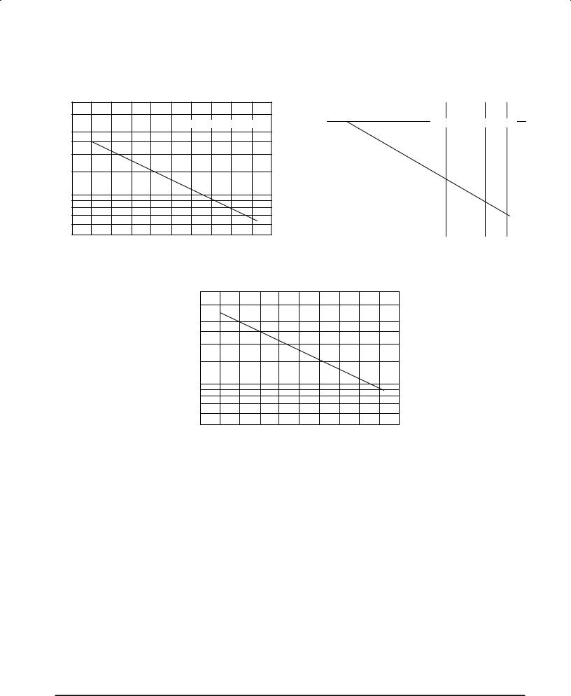
FIGURE 7 Ð GATE TRIGGER CURRENT |
FIGURE 8 Ð GATE TRIGGER VOLTAGE |
GT
I , GATE TRIGGER CURRENT (mA)
50
40
OFF-STATE VOLTAGE = 12 V
30
20
10
7.0
5.0 ±60 ±40 ±20 0 20 40 60 80 100 120 140
TJ, JUNCTION TEMPERATURE (°C)
V , GATE TRIGGER VOLTAGE (VOLTS) GT
1.1 |
|
|
|
|
|
|
|
|
|
|
|
|
|
|
|
|
|
|
|
1.0 |
|
|
|
|
|
|
|
|
|
|
|
OFF- |
STATE |
VOLTAGE = 12 V |
|
|
|||
0.9 |
|
|
|
|
|
|
|
|
|
|
|
|
|
|
|
|
|
|
|
|
|
|
|
|
|
|
|
|
|
|
|
|
|
|
|
|
|
|
|
|
|
|
|
|
|
|
|
|
|
|
|
|
|
|
|
|
|
|
|
0.8 |
|
|
|
|
|
|
|
|
|
|
|
|
|
|
|
|
|
|
|
|
|
|
|
|
|
|
|
|
|
|
|
|
|
|
|
|
|
|
|
|
|
|
|
|
|
|
|
|
|
|
|
|
|
|
|
|
|
|
|
0.7 |
|
|
|
|
|
|
|
|
|
|
|
|
|
|
|
|
|
|
|
|
|
|
|
|
|
|
|
|
|
|
|
|
|
|
|
|
|
|
|
|
|
|
|
|
|
|
|
|
|
|
|
|
|
|
|
|
|
|
|
0.6 |
|
|
|
|
|
|
|
|
|
|
|
|
|
|
|
|
|
|
|
|
|
|
|
|
|
|
|
|
|
|
|
|
|
|
|
|
|
|
|
|
|
|
|
|
|
|
|
|
|
|
|
|
|
|
|
|
|
|
|
0.5 |
|
|
|
|
|
|
|
|
|
|
|
|
|
|
|
|
|
|
|
|
|
|
|
|
|
|
|
|
|
|
|
|
|
|
|
|
|
|
|
|
|
|
|
|
|
|
|
|
|
|
|
|
|
|
|
|
|
|
|
0.4 |
|
|
|
|
|
|
|
|
|
|
|
|
|
|
|
|
|
|
|
|
|
|
|
|
|
|
|
|
|
|
|
|
|
|
|
|
|
|
|
±60 |
±40 |
±20 |
0 |
20 |
40 |
60 |
80 |
100 |
120 |
140 |
|||||||||
|
|
|
|
|
|
TJ, JUNCTION TEMPERATURE (°C) |
|
|
|
|
|||||||||
FIGURE 9 Ð HOLDING CURRENT
IH, HOLDING CURRENT (mA)
50
40
30
20
10
7.0
5.0
±60 |
±40 |
±20 |
0 |
20 |
40 |
60 |
80 |
100 |
120 |
140 |
TJ, JUNCTION TEMPERATURE (°C)
4 |
Motorola Thyristor Device Data |
2N6504 thru 2N6509
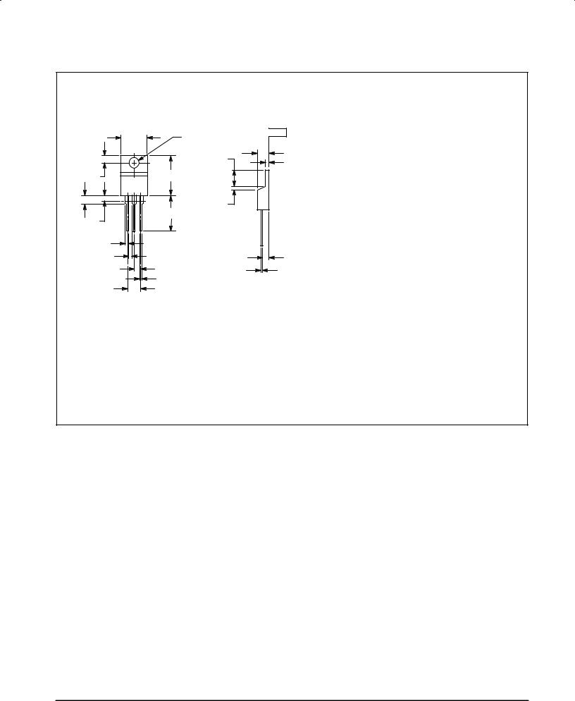
PACKAGE DIMENSIONS
|
B |
±T± |
PLANESEATING |
|
|
F |
|
|
|
|
|
C |
|
|
|
|
T |
S |
|
|
|
4 |
|
|
Q |
|
|
|
|
|
A |
|
|
|
1 |
2 |
3 |
|
|
H |
|
|
STYLE 3: |
|
|
U |
PIN 1. |
CATHODE |
|
|
|
|||
|
|
K |
2. |
ANODE |
Z |
|
3. |
GATE |
|
|
|
|||
|
|
4. |
ANODE |
|
L |
|
|
|
|
V |
|
|
R |
|
G |
|
J |
|
|
|
|
D |
|
|
|
N |
|
|
|
NOTES:
1.DIMENSIONING AND TOLERANCING PER ANSI Y14.5M, 1982.
2.CONTROLLING DIMENSION: INCH.
3.DIMENSION Z DEFINES A ZONE WHERE ALL BODY AND LEAD IRREGULARITIES ARE ALLOWED.
|
INCHES |
MILLIMETERS |
||
DIM |
MIN |
MAX |
MIN |
MAX |
A |
0.570 |
0.620 |
14.48 |
15.75 |
B |
0.380 |
0.405 |
9.66 |
10.28 |
C |
0.160 |
0.190 |
4.07 |
4.82 |
D |
0.025 |
0.035 |
0.64 |
0.88 |
F |
0.142 |
0.147 |
3.61 |
3.73 |
G |
0.095 |
0.105 |
2.42 |
2.66 |
H |
0.110 |
0.155 |
2.80 |
3.93 |
J |
0.014 |
0.022 |
0.36 |
0.55 |
K |
0.500 |
0.562 |
12.70 |
14.27 |
L |
0.045 |
0.055 |
1.15 |
1.39 |
N |
0.190 |
0.210 |
4.83 |
5.33 |
Q |
0.100 |
0.120 |
2.54 |
3.04 |
R |
0.080 |
0.110 |
2.04 |
2.79 |
S |
0.045 |
0.055 |
1.15 |
1.39 |
T |
0.235 |
0.255 |
5.97 |
6.47 |
U |
0.000 |
0.050 |
0.00 |
1.27 |
V |
0.045 |
±±± |
1.15 |
±±± |
Z |
±±± |
0.080 |
±±± |
2.04 |
CASE 221A-04 (TO±220AB)
Motorola Thyristor Device Data |
5 |

2N6504 thru 2N6509
Motorola reserves the right to make changes without further notice to any products herein. Motorola makes no warranty, representation or guarantee regarding the suitability of its products for any particular purpose, nor does Motorola assume any liability arising out of the application or use of any product or circuit, and specifically disclaims any and all liability, including without limitation consequential or incidental damages. ªTypicalº parameters can and do vary in different applications. All operating parameters, including ªTypicalsº must be validated for each customer application by customer's technical experts. Motorola does not convey any license under its patent rights nor the rights of others. Motorola products are not designed, intended, or authorized for use as components in systems intended for surgical implant into the body, or other applications intended to support or sustain life, or for any other application in which the failure of the Motorola product could create a situation where personal injury or death may occur. Should Buyer purchase or use Motorola products for any such unintended or unauthorized application, Buyer shall indemnify and hold Motorola and its officers, employees, subsidiaries, affiliates, and distributors harmless against all claims, costs, damages, and expenses, and reasonable attorney fees arising out of, directly or indirectly, any claim of personal injury or death associated with such unintended or unauthorized use, even if such claim alleges that Motorola was negligent regarding the design or manufacture of the part. Motorola and  are registered trademarks of Motorola, Inc. Motorola, Inc. is an Equal Opportunity/Affirmative Action Employer.
Literature Distribution Centers:
USA: Motorola Literature Distribution; P.O. Box 20912; Phoenix, Arizona 85036.
EUROPE: Motorola Ltd.; European Literature Centre; 88 Tanners Drive, Blakelands, Milton Keynes, MK14 5BP, England. JAPAN: Nippon Motorola Ltd.; 4-32-1, Nishi-Gotanda, Shinagawa-ku, Tokyo 141, Japan.
ASIA PACIFIC: Motorola Semiconductors H.K. Ltd.; Silicon Harbour Center, No. 2 Dai King Street, Tai Po Industrial Estate, Tai Po, N.T., Hong Kong.
◊ |
2N6504/D |
*2N6504/D*