

MOTOROLA
SEMICONDUCTOR TECHNICAL DATA
Order this document by MCR12DCM/D
Silicon Controlled Rectifiers
Reverse Blocking Thyristors
Designed for high volume, low cost, industrial and consumer applications such as motor control; process control; temperature, light and speed control.
• Small Size |
|
• Passivated Die for Reliability and Uniformity |
|
• Low Level Triggering and Holding Characteristics |
A |
• Available in Two Package Styles |
|
Surface Mount Lead Form Ð Case 369A |
|
Miniature Plastic Package Ð Straight Leads Ð Case 369 |
|
ORDERING INFORMATION |
G |
• To Obtain ªDPAKº in Surface Mount Leadform (Case 369A) |
|
Shipped in Sleeves Ð No Suffix, i.e. MCR12DCN |
K |
Shipped in 16 mm Tape and Reel Ð Add ªT4º Suffix to Device Number, |
|
i.e. MCR12DCNT4 |
|
• To Obtain ªDPAKº in Straight Lead Version (Case 369) Shipped in Sleeves Ð Add ª±1º Suffix to Device Number, i.e. MCR12DCN±1
MAXIMUM RATINGS (TJ = 25°C unless otherwise noted)
MCR12DCM
MCR12DCN
Motorola Preferred Devices
SCRs
12 AMPERES RMS
600 thru 800 VOLTS
A
K 

A G
CASE 369A±13
STYLE 4
Rating |
|
Symbol |
Value |
Unit |
|
|
|
|
|
Peak Repetitive Off±State Voltage (1) |
|
V |
|
Volts |
|
|
DRM |
|
|
Peak Repetitive Reverse Voltage |
|
VRRM |
|
|
(TJ = ±40 to 125°C) |
MCR12DCM |
|
600 |
|
|
MCR12DCN |
|
800 |
|
|
|
|
|
|
On±State RMS Current |
|
IT(RMS) |
|
Amps |
(All Conduction Angles; TC = 90°C) |
|
|
12 |
|
Average On±State Current (All Conduction Angles; TC = 90°C) |
IT(AV) |
7.6 |
|
|
Peak Non±Repetitive Surge Current |
|
ITSM |
|
|
(One Half Cycle, 60 Hz, TJ = 125°C) |
|
|
100 |
|
Circuit Fusing Consideration (t = 8.3 msec) |
|
I2t |
41 |
A2sec |
Peak Gate Power |
|
PGM |
|
Watts |
(Pulse Width ≤ 10 msec, TC = 90°C) |
|
|
5.0 |
|
Average Gate Power |
|
PG(AV) |
|
|
(t = 8.3 msec, TC = 90°C) |
|
|
0.5 |
|
Peak Gate Current (Pulse Width ≤ 10 sec,m |
TC = 90°C) |
IGM |
2.0 |
Amps |
Operating Junction Temperature Range |
|
TJ |
±40 to 125 |
°C |
Storage Temperature Range |
|
Tstg |
±40 to 150 |
|
THERMAL CHARACTERISTICS |
|
|
|
|
Characteristic |
Symbol |
Max |
Unit |
|
|
|
|
Thermal Resistance Ð Junction to Case |
RqJC |
2.2 |
°C/W |
Ð Junction to Ambient |
RqJA |
88 |
|
Ð Junction to Ambient (2) |
RqJA |
80 |
|
Maximum Lead Temperature for Soldering Purposes (3) |
T |
260 |
°C |
|
L |
|
|
(1)VDRM for all types can be applied on a continuous basis. Ratings apply for zero or negative gate voltage; positive gate voltage shall not be applied concurrent with negative potential on the anode. Blocking voltages shall not be tested with a constant current source such that the voltage ratings of the device are exceeded.
(2)Surface mounted on minimum recommended pad size.
(3)1/8″ from case for 10 seconds.
Preferred devices are Motorola recommended choices for future use and best overall value.
Motorola Thyristor Device Data
Motorola, Inc. 1997

MCR12DCM MCR12DCN
ELECTRICAL CHARACTERISTICS (TJ = 25°C unless otherwise noted)
Characteristics |
|
Symbol |
Min |
Typ |
Max |
Unit |
|
|
|
|
|
|
|
Peak Forward Blocking Current |
|
IDRM |
|
|
|
mA |
Peak Reverse Blocking Current |
TJ = 25°C |
IRRM |
|
|
|
|
(VAK = Rated VDRM or VRRM, Gate Open) |
|
Ð |
Ð |
0.01 |
|
|
|
TJ = 125°C |
|
Ð |
Ð |
5.0 |
|
Peak On±State Voltage (1) |
|
V |
|
|
|
Volts |
(ITM = 24 A) |
|
TM |
Ð |
1.4 |
2.1 |
|
|
|
|
||||
Gate Trigger Current (Continuous dc) |
|
IGT |
|
|
|
mA |
(VD = 12 V, RL = 100 W, TJ = 25°C) |
|
|
2.0 |
7.0 |
20 |
|
(VD = 12 V, RL = 100 W, TJ = ±40°C) |
|
|
Ð |
Ð |
40 |
|
Gate Trigger Voltage (Continuous dc) |
|
VGT |
|
|
|
Volts |
(VD = 12 V, RL = 100 W, TJ = 25°C) |
|
|
0.5 |
0.65 |
1.0 |
|
(VD = 12 V, RL = 100 W, TJ = ±40°C) |
|
|
Ð |
Ð |
2.0 |
|
(VD = 12 V, RL = 100 W, TJ = 125°C) |
|
|
0.2 |
Ð |
Ð |
|
Holding Current |
|
IH |
|
|
|
mA |
(VD = 12 V, IT = 200 mA, TJ = 25°C) |
|
|
4.0 |
22 |
40 |
|
(VD = 12 V, IT = 200 mA, TJ = ±40°C) |
|
|
Ð |
Ð |
80 |
|
Latching Current |
|
IL |
|
|
|
mA |
(VD = 12 V, IG = 20 mA, TJ = 25°C) |
|
|
4.0 |
22 |
40 |
|
(VD = 12 V, IG = 40 mA, TJ = ±40°C) |
|
|
Ð |
Ð |
80 |
|
DYNAMIC CHARACTERISTICS |
|
|
|
|
|
|
Characteristics |
Symbol |
Min |
Typ |
Max |
Unit |
|
|
|
|
|
|
Critical Rate of Rise of Off±State Voltage |
dv/dt |
|
|
|
V/ms |
(VD = Rated VDRM, Exponential Waveform, Gate Open, TJ = 125°C) |
|
50 |
200 |
Ð |
|
(1) Pulse Test; Pulse Width ≤ 2.0 msec, Duty Cycle ≤ 2%.
2 |
Motorola Thyristor Device Data |

°C) |
125 |
|
|
|
|
|
|
|
|
|
|
|
|
|
|
|
|
|
|
( |
|
|
|
|
|
|
|
|
|
TEMPERATURE |
120 |
|
|
|
|
|
|
|
|
115 |
|
|
|
|
|
|
|
|
|
110 |
|
|
|
|
|
|
|
|
|
|
|
|
|
|
|
|
|
|
|
CASE |
105 |
|
|
|
|
|
|
|
|
|
|
|
|
|
|
|
dc |
|
|
ALLOWABLE |
100 |
a |
|
|
|
|
|
|
|
|
|
|
|
|
|
|
|||
95 |
a = Conduction |
|
|
|
|
|
|
||
90 |
Angle |
|
|
|
|
|
|
|
|
MAXIMUM |
|
a = 30° |
60° |
90° |
120° |
180° |
|
||
85 |
|
|
|||||||
1.0 |
2.0 |
3.0 |
|
|
|
|
|
||
0 |
4.0 |
5.0 |
6.0 |
7.0 |
8.0 |
||||
, |
|
|
|
|
|
|
|
|
|
C |
|
IT(AV), AVERAGE ON±STATE CURRENT (AMPS) |
|
||||||
T |
|
|
|||||||
|
|
|
|
|
MCR12DCM |
MCR12DCN |
|||
(WATTS) |
16 |
|
|
|
|
|
|
|
180° |
|
|
|
|
|
|
|
|
||
14 |
|
|
|
|
90° |
120° |
|
|
|
DISSIPATION |
12 |
|
|
|
|
|
|
|
|
|
a |
|
|
60° |
|
|
dc |
||
|
a = Conduction |
|
|
|
|
|
|||
10 |
|
|
|
|
|
|
|||
|
Angle |
|
|
|
|
|
|
||
POWER |
8.0 |
|
a = 30° |
|
|
|
|
|
|
|
|
|
|
|
|
|
|
||
6.0 |
|
|
|
|
|
|
|
|
|
, AVERAGE |
4.0 |
|
|
|
|
|
|
|
|
2.0 |
|
|
|
|
|
|
|
|
|
(AV) |
0 |
|
|
|
|
|
|
|
|
P |
1.0 |
2.0 |
3.0 |
4.0 |
5.0 |
6.0 |
7.0 |
8.0 |
|
|
0 |
||||||||
|
|
IT(AV), AVERAGE ON±STATE CURRENT (AMPS) |
|
||||||
Figure 1. Average Current Derating |
Figure 2. On±State Power Dissipation |
IT, INSTANTANEOUS ON±STATE CURRENT (AMPS)
100 |
TYPICAL @ TJ = 25°C |
|
|
|
|
1.0 |
|
|
|
|
|
|
|
|
|
|
|
|
|
|
|
|
|
||
|
|
|
MAXIMUM @ TJ = 125°C |
(NORMALIZED) |
|
|
|
|
|
|
||
10 |
|
|
|
|
RESISTANCETRANSIENT |
|
|
|
|
|
|
|
|
|
|
|
|
|
|
|
|
|
|
|
|
|
|
|
|
|
|
|
0.1 |
|
|
|
|
|
|
|
MAXIMUM @ TJ = 25°C |
|
|
|
|
|
|
|
S |
r(t) |
|
1.0 |
|
|
|
|
|
|
|
|
|
ZqJC(t) = RqJC(t) |
||
|
|
|
|
|
|
|
|
|
|
|
|
|
|
|
|
|
|
, |
|
|
|
|
|
|
|
|
|
|
|
|
(t) |
|
|
|
|
|
|
|
|
|
|
|
|
r |
|
|
|
|
|
|
|
0.1 |
|
|
|
|
|
|
0.01 |
|
|
|
|
|
0 |
1.0 |
2.0 |
3.0 |
4.0 |
5.0 |
|
0.1 |
1.0 |
10 |
100 |
1000 |
10 K |
|
VT, INSTANTANEOUS ON±STATE VOLTAGE (VOLTS) |
|
|
|
|
t, TIME (ms) |
|
|
||||
Figure 3. On±State Characteristics |
Figure 4. Transient Thermal Response |
IGT, GATE TRIGGER CURRENT (mA)
100
10
1.0 |
|
|
|
|
35 |
|
|
|
|
|
|
±40 |
±25 |
±10 |
5.0 |
20 |
50 |
65 |
80 |
95 |
110 |
125 |
TJ, JUNCTION TEMPERATURE (°C)
Figure 5. Typical Gate Trigger Current versus Junction Temperature
VGT, GATE TRIGGER VOLTAGE (VOLTS)
0.9
0.8
0.7
0.6
0.5
0.4
0.3
0.2
±40 |
±25 |
±10 |
5.0 |
20 |
35 |
50 |
65 |
80 |
95 |
110 |
125 |
|
|
|
TJ, JUNCTION TEMPERATURE (°C) |
|
|
|
|||||
Figure 6. Typical Gate Trigger Voltage versus Junction Temperature
Motorola Thyristor Device Data |
3 |

MCR12DCM MCR12DCN
CURRENT (mA) |
100 |
|
|
|
|
|
|
|
|
|
|
|
|
|
|
|
|
|
|
|
|
|
|
|
10 |
|
|
|
|
|
|
|
|
|
|
|
|
|
|
|
|
|
|
|
|
|
|
|
|
|
|
|
|
|
|
|
|
|
|
|
|
|
|
|
|
|
|
|
|
|
|
|
||
|
|
|
|
|
|
|
|
|
|
|
|
|
|
|
|
|
|
|
|
|
|
|
||
|
|
|
|
|
|
|
|
|
|
|
|
|
|
|
|
|
|
|
|
|
|
|
||
|
|
|
|
|
|
|
|
|
|
|
|
|
|
|
|
|
|
|
|
|
|
|
||
|
|
|
|
|
|
|
|
|
|
|
|
|
|
|
|
|
|
|
|
|
|
|
||
|
|
|
|
|
|
|
|
|
|
|
|
|
|
|
|
|
|
|
|
|
|
|
||
|
|
|
|
|
|
|
|
|
|
|
|
|
|
|
|
|
|
|
|
|
|
|
||
, HOLDING |
|
|
|
|
|
|
|
|
|
|
|
|
|
|
|
|
|
|
|
|
|
|
|
|
|
|
|
|
|
|
|
|
|
|
|
|
|
|
|
|
|
|
|
|
|
|
|
|
|
|
|
|
|
|
|
|
|
|
|
|
|
|
|
|
|
|
|
|
|
|
|
|
|
|
|
|
|
|
|
|
|
|
|
|
|
|
|
|
|
|
|
|
|
|
|
|
|
|
|
|
|
|
|
|
|
|
|
|
|
|
|
|
|
|
|
|
|
|
|
|
|
|
|
|
|
|
|
|
|
|
|
|
|
|
|
|
|
|
|
|
|
|
|
|
|
|
|
|
|
H |
|
|
|
|
|
|
|
|
|
|
|
|
|
|
|
|
|
|
|
|
|
|
|
|
I |
|
|
|
|
|
|
|
|
|
|
|
|
|
|
|
|
|
|
|
|
|
|
|
|
|
1.0 |
|
|
|
|
|
|
|
|
|
|
|
|
|
|
|
|
|
|
|
|
|
|
|
|
|
|
|
|
|
|
|
|
|
|
|
|
|
|
|
|
|
|
|
|
|
|
|
|
|
|
|
|
±10 |
|
|
|
|
35 |
|
|
|
|
80 |
|
|
|
|
|
|
||||
|
±40 |
±25 |
5.0 |
20 |
50 |
65 |
95 |
110 |
125 |
|||||||||||||||
TJ, JUNCTION TEMPERATURE (°C)
Figure 7. Typical Holding Current versus
Junction Temperature
CURRENT (mA) |
100 |
|
|
|
|
|
|
|
|
|
|
|
|
|
|
|
|
|
|
|
|
|
|
|
10 |
|
|
|
|
|
|
|
|
|
|
|
|
|
|
|
|
|
|
|
|
|
|
|
|
|
|
|
|
|
|
|
|
|
|
|
|
|
|
|
|
|
|
|
|
|
|
|
||
|
|
|
|
|
|
|
|
|
|
|
|
|
|
|
|
|
|
|
|
|
|
|
||
|
|
|
|
|
|
|
|
|
|
|
|
|
|
|
|
|
|
|
|
|
|
|
||
|
|
|
|
|
|
|
|
|
|
|
|
|
|
|
|
|
|
|
|
|
|
|
||
|
|
|
|
|
|
|
|
|
|
|
|
|
|
|
|
|
|
|
|
|
|
|
||
|
|
|
|
|
|
|
|
|
|
|
|
|
|
|
|
|
|
|
|
|
|
|
||
|
|
|
|
|
|
|
|
|
|
|
|
|
|
|
|
|
|
|
|
|
|
|
||
, LATCHING |
|
|
|
|
|
|
|
|
|
|
|
|
|
|
|
|
|
|
|
|
|
|
|
|
|
|
|
|
|
|
|
|
|
|
|
|
|
|
|
|
|
|
|
|
|
|
|
|
|
|
|
|
|
|
|
|
|
|
|
|
|
|
|
|
|
|
|
|
|
|
|
|
|
|
|
|
|
|
|
|
|
|
|
|
|
|
|
|
|
|
|
|
|
|
|
|
|
|
|
|
|
|
|
|
|
|
|
|
|
|
|
|
|
|
|
|
|
|
|
|
|
|
|
|
|
|
|
|
|
|
|
|
|
|
|
|
|
|
|
|
|
|
|
|
|
|
|
|
|
|
|
|
|
|
|
|
|
|
|
|
|
|
|
|
|
|
|
|
|
|
|
|
|
|
L |
|
|
|
|
|
|
|
|
|
|
|
|
|
|
|
|
|
|
|
|
|
|
|
|
I |
|
|
|
|
|
|
|
|
|
|
|
|
|
|
|
|
|
|
|
|
|
|
|
|
|
1.0 |
|
|
|
|
|
|
|
|
|
|
|
|
|
|
|
|
|
|
|
|
|
|
|
|
|
|
|
|
|
|
|
|
|
|
|
|
|
|
|
|
|
|
|
|
|
|
|
|
|
|
|
|
|
|
|
|
|
|
|
|
|
|
|
|
|
|
|
|
|
|
|
|
|
|
±40 |
±25 |
±10 |
5.0 |
20 |
35 |
50 |
65 |
80 |
95 |
110 |
125 |
||||||||||||
TJ, JUNCTION TEMPERATURE (°C)
Figure 8. Typical Latching Current versus
Junction Temperature
1000 |
|
|
|
|
|
|
VD = 800 V |
|
|
|
TJ = 125°C |
s) |
|
|
|
m |
|
|
|
STATIC dv/dt (V/ |
|
|
|
100 |
|
|
|
10 |
100 |
1000 |
10 K |
RGK, GATE±CATHODE RESISTANCE (OHMS)
Figure 9. Exponential Static dv/dt versus
Gate±Cathode Resistance
4 |
Motorola Thyristor Device Data |
MCR12DCM MCR12DCN
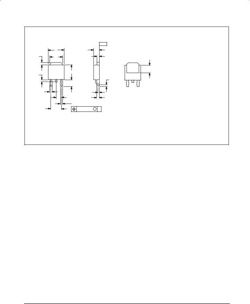
PACKAGE DIMENSIONS
±T± SEATINGPLANE
|
B |
C |
V |
R |
E |
|
4 |
|
Z |
|
|
|
|
S |
|
|
A |
|
|
|
|
1 |
2 |
3 |
U |
|
|
|
|
|
|
|
K |
F |
|
|
J |
|
|
L |
H |
|
|
|
D 2 PL
G |
0.13 (0.005) M T |
NOTES:
1.DIMENSIONING AND TOLERANCING PER ANSI Y14.5M, 1982.
2.CONTROLLING DIMENSION: INCH.
|
INCHES |
MILLIMETERS |
||
DIM |
MIN |
MAX |
MIN |
MAX |
A |
0.235 |
0.250 |
5.97 |
6.35 |
B |
0.250 |
0.265 |
6.35 |
6.73 |
C |
0.086 |
0.094 |
2.19 |
2.38 |
D |
0.027 |
0.035 |
0.69 |
0.88 |
E |
0.033 |
0.040 |
0.84 |
1.01 |
F |
0.037 |
0.047 |
0.94 |
1.19 |
G |
0.180 BSC |
4.58 BSC |
||
H |
0.034 |
0.040 |
0.87 |
1.01 |
J |
0.018 |
0.023 |
0.46 |
0.58 |
K |
0.102 |
0.114 |
2.60 |
2.89 |
L |
0.090 BSC |
2.29 BSC |
||
R |
0.175 |
0.215 |
4.45 |
5.46 |
S |
0.020 |
0.050 |
0.51 |
1.27 |
U |
0.020 |
±±± |
0.51 |
±±± |
V |
0.030 |
0.050 |
0.77 |
1.27 |
Z |
0.138 |
±±± |
3.51 |
±±± |
STYLE 4:
PIN 1. CATHODE
2. ANODE
3. GATE
4. ANODE
CASE 369A±13
ISSUE Y
Motorola Thyristor Device Data |
5 |

MCR12DCM MCR12DCN
Motorola reserves the right to make changes without further notice to any products herein. Motorola makes no warranty, representation or guarantee regarding the suitability of its products for any particular purpose, nor does Motorola assume any liability arising out of the application or use of any product or circuit, and specifically disclaims any and all liability, including without limitation consequential or incidental damages. ªTypicalº parameters which may be provided in Motorola data sheets and/or specifications can and do vary in different applications and actual performance may vary over time. All operating parameters, including ªTypicalsº must be validated for each customer application by customer's technical experts. Motorola does not convey any license under its patent rights nor the rights of others. Motorola products are not designed, intended, or authorized for use as components in systems intended for surgical implant into the body, or other applications intended to support or sustain life, or for any other application in which the failure of the Motorola product could create a situation where personal injury or death may occur. Should Buyer purchase or use Motorola products for any such unintended or unauthorized application, Buyer shall indemnify and hold Motorola and its officers, employees, subsidiaries, affiliates, and distributors harmless against all claims, costs, damages, and expenses, and reasonable attorney fees arising out of, directly or indirectly, any claim of personal injury or death associated with such unintended or unauthorized use, even if such claim alleges that Motorola was negligent regarding the design or manufacture of the part. Motorola and  are registered trademarks of Motorola, Inc. Motorola, Inc. is an Equal Opportunity/Affirmative Action Employer.
|
Mfax is a trademark of Motorola, Inc. |
How to reach us: |
|
USA / EUROPE / Locations Not Listed: Motorola Literature Distribution; |
JAPAN: Nippon Motorola Ltd.: SPD, Strategic Planning Office, 4±32±1, |
P.O. Box 5405, Denver, Colorado 80217. 303±675±2140 or 1±800±441±2447 |
Nishi±Gotanda, Shinagawa±ku, Tokyo 141, Japan. 81±3±5487±8488 |
Mfax : RMFAX0@email.sps.mot.com ± TOUCHTONE 602±244±6609 |
ASIA/PACIFIC: Motorola Semiconductors H.K. Ltd.; 8B Tai Ping Industrial Park, |
± US & Canada ONLY 1±800±774±1848 51 Ting Kok Road, Tai Po, N.T., Hong Kong. 852±26629298
INTERNET: http://motorola.com/sps
6 |
◊ |
Motorola Thyristor Device Data |
|
MCR12DCM/D |