

MOTOROLA
SEMICONDUCTOR TECHNICAL DATA
Order this document by T2322/D
Sensitive Gate Triacs
Silicon Bidirectional Triode Thyristors
. . . designed primarily for ac power switching. The gate sensitivity of these triacs permits the use of economical transistorized or integrated circuit control circuits, and it enhances their use in low-power phase control and load-switching applications.
•Very High Gate Sensitivity
•Low On-State Voltage at High Current Levels
•Glass-Passivated Chip for Stability
•Small, Rugged Thermopad Construction for Low Thermal Resistance, High Heat Dissipation and Durability
T2322
T2323
Series*
*Motorola preferred devices
SENSITIVE GATE TRIACs 2.5 AMPERES RMS 200 thru 600 VOLTS
|
|
|
|
|
|
|
|
|
|
|
G |
|
|
|
|
|
|
|
|
|
|
|
|
|
|
||
|
|
|
|
|
|
|
|
|
|
|
MT2 |
|
|
|
|
|
|
|
|
|
|
|
|
|
MT1 |
|
|
|
|
|
|
|
|
|
|
|
|
|
|
||
|
MT2 |
|
|
|
|
|
|
MT1 |
|
|
CASE 77-08 |
|
|
|
|
|
|
|
|
|
|
|
|
||||
|
|
|
|
|
|
|
G |
|
|
(TO-225AA) |
|
||
|
|
|
|
|
|
|
|
|
|
||||
|
|
|
|
|
|
|
|
|
STYLE 5 |
|
|||
|
|
|
|
|
|
|
|
|
|
|
|
||
|
|
|
|
|
|
|
|
|
|
|
|
|
|
MAXIMUM RATINGS (TJ = 25°C unless otherwise noted.) |
|
|
|
|
|
|
|
|
|
|
|
||
Rating |
Suffix |
|
Symbol |
Value |
|
Unit |
|||||||
|
|
|
|
|
|
|
|
|
|
|
|
|
|
Peak Repetitive Off-State Voltage(1) |
B |
|
|
V |
200 |
|
Volts |
||||||
(TJ = 25 to 100°C, Gate Open) |
D |
|
|
DRM |
400 |
|
|
||||||
|
|
|
|
|
|
|
|||||||
T2322, T2323 |
M |
|
|
|
|
|
600 |
|
|
||||
|
|
|
|
|
|
|
|
|
|
|
|
|
|
RMS On-State Current (TC = 70°C) |
|
|
|
|
IT(RMS) |
2.5 |
|
Amps |
|||||
(Full-Cycle Sine Wave 50 to 60 Hz) |
|
|
|
|
|
|
|
|
|
|
|
||
|
|
|
|
|
|
|
|
|
|
|
|
|
|
Peak Non-repetitive Surge Current |
|
|
|
|
|
ITSM |
25 |
|
Amps |
||||
(One Full Cycle, 60 Hz) |
|
|
|
|
|
|
|
|
|
|
|
||
|
|
|
|
|
|
|
|
|
|
|
|
|
|
Circuit Fusing |
|
|
|
|
|
I2t |
2.6 |
|
A2s |
||||
(t = 8.3 ms) |
|
|
|
|
|
|
|
|
|
|
|
||
|
|
|
|
|
|
|
|
|
|
|
|
|
|
Peak Gate Power (1 μs) |
|
|
|
|
|
PGM |
10 |
|
Watts |
||||
Average Gate Power (TC = 60°C + 38.3 ms) |
|
|
|
|
PG(AV) |
0.15 |
|
Watt |
|||||
Peak Gate Current (1 μs) |
|
|
|
|
|
IGM |
0.5 |
|
Amp |
||||
Operating Junction Temperature Range |
|
|
|
|
|
TJ |
±40 to +110 |
|
°C |
||||
Storage Temperature Range |
|
|
|
|
|
Tstg |
±40 to +150 |
|
°C |
||||
Mounting Torque (6-32 Screw)(2) |
|
|
|
Ð |
|
|
8 |
|
in. lb. |
||||
1.VDRM for all types can be applied on a continuous basis. Blocking voltages shall not be tested with a constant current source such that the voltage ratings of the devices are exceeded.
2.Torque rating applies with use of torque washer (Shakeproof WD19523 or equivalent). Mounting Torque in excess of 6 in. lb. does not
appreciably lower case-to-sink thermal resistance. Main terminal 2 and heat-sink contact pad are common.
For soldering purposes (either terminal connection or device mounting), soldering temperatures shall not exceed +200°C, for 10 seconds. Consult factory for lead bending options.
Preferred devices are Motorola recommended choices for future use and best overall value.
Motorola, Inc. 1995

T2322 T2323 Series
THERMAL CHARACTERISTICS
Characteristic |
|
|
|
Symbol |
|
Max |
|
|
Unit |
|||
|
|
|
|
|
|
|
|
|
|
|
|
|
Thermal Resistance, Junction to Case |
|
|
|
RθJC |
|
3.5 |
|
|
°C/W |
|||
Thermal Resistance, Junction to Ambient |
|
|
|
RθJA |
|
60 |
|
|
°C/W |
|||
ELECTRICAL CHARACTERISTICS (TC = 25°C and either polarity of MT2 to MT1 voltage unless otherwise noted.) |
|
|
|
|
||||||||
Characteristic |
|
Symbol |
|
Min |
Typ |
Max |
|
Unit |
||||
|
|
|
|
|
|
|
|
|
|
|
|
|
Peak Blocking Current |
TJ = 25°C |
|
IDRM |
|
Ð |
|
Ð |
10 |
|
μA |
||
(VD = Rated VDRM, Gate Open) |
|
|
|
|
|
|
||||||
|
TJ = 100°C |
|
|
|
|
Ð |
|
0.2 |
0.75 |
|
mA |
|
Peak On-State Voltage* |
|
|
VTM |
|
Ð |
|
1.7 |
2.6 |
|
Volts |
||
(ITM = 10 A) |
T2323 Series |
|
|
|
|
|
|
|||||
|
T2322 Series |
|
|
|
Ð |
|
1.7 |
2.2 |
|
|
||
|
|
|
|
|
|
|
|
|
|
|
|
|
Gate Trigger Current (Continuous dc) |
|
|
IGT |
|
|
|
|
|
|
|
mA |
|
(VD = 12 V, RL = 30 Ω) |
|
|
|
|
|
|
|
|
|
|
|
|
All Modes |
|
T2322 Series |
|
|
|
Ð |
|
Ð |
10 |
|
|
|
MT2(+), G(+); MT2(±), G(±) |
T2323 Series |
|
|
|
Ð |
|
Ð |
25 |
|
|
||
MT2(+), G(±); MT2(±),I G(+) |
T2323 Series |
|
|
|
Ð |
|
Ð |
40 |
|
|
||
|
|
|
|
|
|
|
|
|
|
|
|
|
Gate Trigger Voltage (Continuous dc) |
|
|
VGT |
|
|
|
|
|
|
|
Volts |
|
(VD = 12 Vdc, RL = 30 Ω, TC = 25°C) |
|
|
|
|
Ð |
|
1 |
2.2 |
|
|
||
(VD = VDRM, RL = 125 Ω, TC = 100°C) |
|
|
|
|
0.15 |
Ð |
Ð |
|
|
|||
Holding Current |
|
|
IH |
|
Ð |
|
15 |
30 |
|
mA |
||
(VD = 12 V, ITM = 150 mA, Gate Open) |
|
|
|
|
|
|
|
|
|
|
|
|
Gate Controlled Turn-On Time |
|
|
tgt |
|
Ð |
|
1.8 |
2.5 |
|
μs |
||
(VD = Rated VDRM, ITM = 10 A pk, IG = 60 mA) |
|
|
|
|
|
|
|
|
|
|
|
|
Critical Rate-of-Rise of Off-State Voltage |
|
dv/dt |
|
10 |
|
100 |
Ð |
|
V/μs |
|||
(VD = Rated VDRM, Exponential Waveform, TC = 100°C) |
|
|
|
|
|
|
|
|
|
|
||
Critical Rate-of-Rise of Commutation Voltage |
|
dv/dt(c) |
|
1 |
|
4 |
Ð |
|
V/μs |
|||
(VD = Rated VDRM, ITM = 3.5 A pk, Commutating |
|
|
|
|
|
|
|
|
|
|
|
|
di/dt = 1.26 A/ms, Gate Unenergized, TC = 90°C) |
|
|
|
|
|
|
|
|
|
|
|
|
*Pulse Test: Pulse Width p 300 μs, Duty Cycle p 2%. |
|
|
|
|
|
|
|
|
|
|
|
|
2 |
Motorola Thyristor Device Data |
T2322 T2323 Series
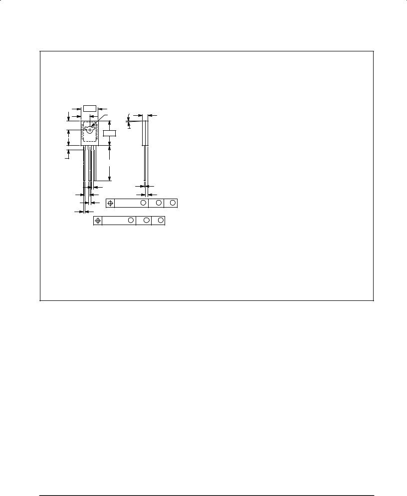
PACKAGE DIMENSIONS
±B± |
|
||
U |
|
F |
C |
Q |
|
|
M |
|
|
±A± |
|
|
|
|
|
1 |
2 |
3 |
|
H |
|
K |
|
|
|
|
|
V |
|
J |
|
G |
|
|
R |
S |
0.25 (0.010) M |
A |
M B M |
D 2 PL |
|
|
|
0.25 (0.010) M A M |
B |
M |
|
STYLE 5:
PIN 1. MT 1
2.MT 2
3.GATE
NOTES:
1.DIMENSIONING AND TOLERANCING PER ANSI Y14.5M, 1982.
2.CONTROLLING DIMENSION: INCH.
|
INCHES |
MILLIMETERS |
||
DIM |
MIN |
MAX |
MIN |
MAX |
A |
0.425 |
0.435 |
10.80 |
11.04 |
B |
0.295 |
0.305 |
7.50 |
7.74 |
C |
0.095 |
0.105 |
2.42 |
2.66 |
D |
0.020 |
0.026 |
0.51 |
0.66 |
F |
0.115 |
0.130 |
2.93 |
3.30 |
G |
0.094 BSC |
2.39 BSC |
||
H |
0.050 |
0.095 |
1.27 |
2.41 |
J |
0.015 |
0.025 |
0.39 |
0.63 |
K |
0.575 |
0.655 |
14.61 |
16.63 |
M |
5 |
TYP |
5 |
TYP |
Q |
0.148 |
0.158 |
3.76 |
4.01 |
R |
0.045 |
0.055 |
1.15 |
1.39 |
S |
0.025 |
0.035 |
0.64 |
0.88 |
U |
0.145 |
0.155 |
3.69 |
3.93 |
V |
0.040 |
±±± |
1.02 |
±±± |
CASE 77-08 (TO±225AA)
Motorola Thyristor Device Data |
3 |

T2322 T2323 Series
Motorola reserves the right to make changes without further notice to any products herein. Motorola makes no warranty, representation or guarantee regarding the suitability of its products for any particular purpose, nor does Motorola assume any liability arising out of the application or use of any product or circuit, and specifically disclaims any and all liability, including without limitation consequential or incidental damages. ªTypicalº parameters can and do vary in different applications. All operating parameters, including ªTypicalsº must be validated for each customer application by customer's technical experts. Motorola does not convey any license under its patent rights nor the rights of others. Motorola products are not designed, intended, or authorized for use as components in systems intended for surgical implant into the body, or other applications intended to support or sustain life, or for any other application in which the failure of the Motorola product could create a situation where personal injury or death may occur. Should Buyer purchase or use Motorola products for any such unintended or unauthorized application, Buyer shall indemnify and hold Motorola and its officers, employees, subsidiaries, affiliates, and distributors harmless against all claims, costs, damages, and expenses, and reasonable attorney fees arising out of, directly or indirectly, any claim of personal injury or death associated with such unintended or unauthorized use, even if such claim alleges that Motorola was negligent regarding the design or manufacture of the part. Motorola and  are registered trademarks of Motorola, Inc. Motorola, Inc. is an Equal Opportunity/Affirmative Action Employer.
Literature Distribution Centers:
USA: Motorola Literature Distribution; P.O. Box 20912; Phoenix, Arizona 85036.
EUROPE: Motorola Ltd.; European Literature Centre; 88 Tanners Drive, Blakelands, Milton Keynes, MK14 5BP, England. JAPAN: Nippon Motorola Ltd.; 4-32-1, Nishi-Gotanda, Shinagawa-ku, Tokyo 141, Japan.
ASIA PACIFIC: Motorola Semiconductors H.K. Ltd.; Silicon Harbour Center, No. 2 Dai King Street, Tai Po Industrial Estate, Tai Po, N.T., Hong Kong.
◊ |
T2322/D |
*T2322/D*