

MOTOROLA
SEMICONDUCTOR TECHNICAL DATA
Order this document by MCR08BT1/D
SOT 223 SCR
Silicon Controlled Rectifiers
Reverse Blocking Triode Thyristors
PNPN devices designed for line powered consumer applications such as relay and lamp drivers, small motor controls, gate drivers for larger thyristors, and sensing and detection circuits. Supplied in surface mount package for use in automated manufacturing.
•Sensitive Gate Trigger Current
•Blocking Voltage to 600 Volts
•Glass Passivated Surface for Reliability and Uniformity
•Surface Mount Package
•Devices Supplied on 1 K Reel
MAXIMUM RATINGS (TJ = 25°C unless otherwise noted)
MCR08BT1
Series*
*Motorola preferred devices
SCR
0.8 AMPERE RMS
200 thru 600 Volts
CASE 318E-04 (SOT-223) STYLE 10
Rating |
Symbol |
Value |
Unit |
|
|
|
|
Peak Repetitive Forward and Reverse Blocking Voltage(1) |
VDRM, VRRM |
|
Volts |
(1/2 Sine Wave, RGK = 1000 Ω, TJ = 25 to 110°C) |
|
200 |
|
MCR08BT1 |
|
|
|
MCR08DT1 |
|
400 |
|
MCR08MT1 |
|
600 |
|
|
|
|
|
On-State Current RMS (TC = 80°C) |
IT(RMS) |
0.8 |
Amps |
Peak Non-repetitive Surge Current |
ITSM |
10 |
Amps |
(One Full Cycle, 60 Hz, TC = 25°C) |
|
|
|
Circuit Fusing Considerations (t = 8.3 ms) |
I2t |
0.4 |
A2s |
Peak Gate Power, Forward, TA = 25°C |
PGM |
0.1 |
Watts |
Average Gate Power (TC = 80°C, t = 8.3 ms) |
PG(AV) |
0.01 |
Watts |
Operating Junction Temperature Range |
TJ |
±40 to +110 |
°C |
Storage Temperature Range |
Tstg |
±40 to +150 |
°C |
Maximum Device Temperature for Soldering Purposes (for 10 Seconds Maximum) |
TL |
260 |
°C |
THERMAL CHARACTERISTICS |
|
|
|
Characteristic |
Symbol |
Max |
Unit |
|
|
|
|
Thermal Resistance, Junction to Ambient |
RθJA |
156 |
°C/W |
PCB Mounted per Figure 1 |
|
|
|
|
|
|
|
Thermal Resistance, Junction to Tab |
RθJT |
25 |
°C/W |
Measured on Anode Tab Adjacent to Epoxy |
|
|
|
|
|
|
|
1.VDRM and VRRM for all types can be applied on a continuous basis. Ratings apply for zero or negative gate voltage; however, positive gate voltage shall not be applied concurrent with negative potential on the anode. Blocking voltages shall not be tested with a constant source such that the voltage ratings of the devices are exceeded.
Preferred devices are Motorola recommended choices for future use and best overall value.
REV 1
Motorola, Inc. 1995

MCR08BT1 Series
ELECTRICAL CHARACTERISTICS (TC = 25°C unless otherwise noted, RGK = 1 KΩ)
Characteristic |
|
Symbol |
Min |
Typ |
Max |
Unit |
|
|
|
|
|
|
|
Peak Repetitive Forward or Reverse Blocking Current |
|
IDRM, IRRM |
|
|
|
|
(VAK = Rated VDRM or VRRM, RGK = 1000 Ω) |
TJ = 25°C |
|
Ð |
Ð |
10 |
μA |
|
TJ = 110°C |
|
Ð |
Ð |
200 |
μA |
Maximum On-State Voltage (Either Direction)* |
|
VTM |
Ð |
Ð |
1.7 |
Volts |
(IT = 1.0 A Peak, TA = 25°C) |
|
|
|
|
|
|
Gate Trigger Current (Continuous dc) |
|
IGT |
Ð |
Ð |
200 |
μA |
(Anode Voltage = 7.0 Vdc, RL = 100 Ω) |
|
|
|
|
|
|
Holding Current |
|
IH |
Ð |
Ð |
5.0 |
mA |
(VD = 7.0 Vdc, |
|
|
|
|
|
|
Initializing Current = 20 mA, RGK = 1000 Ω) |
|
|
|
|
|
|
Gate Trigger Voltage (Continuous dc) |
|
VGT |
Ð |
Ð |
0.8 |
Volts |
(Anode Voltage = 7.0 Vdc, RL = 100 Ω) |
|
|
|
|
|
|
Critical Rate-of-Rise of Off State Voltage |
|
dv/dt |
10 |
Ð |
Ð |
V/μs |
(Vpk = Rated VDRM, TC = 110°C, RGK = 1000 Ω, Exponential Method) |
|
|
|
|
|
|
* Pulse Test: Pulse Width ≤ 300 μs, Duty Cycle ≤ 2%. |
|
|
|
|
|
|
|
|
0.15 |
|
|
|
|
|
|
|
3.8 |
|
|
|
|
0.079 |
|
|
|
|
|
|
2.0 |
|
|
|
|
|
|
0.091 |
0.091 |
0.244 |
|
||
|
6.2 |
|
||||
|
2.3 |
|
2.3 |
|
|
|
|
|
|
|
|
||
|
0.079 |
|
|
|
|
|
|
2.0 |
|
|
|
|
|
|
0.059 |
0.059 |
0.059 |
inches |
BOARD MOUNTED VERTICALLY IN CINCH 8840 EDGE CONNECTOR. |
|
|
mm |
|||||
|
1.5 |
|
1.5 |
1.5 |
BOARD THICKNESS = 65 MIL., FOIL THICKNESS = 2.5 MIL. |
|
0.984 |
|
|
||||
25.0 |
|
|
|
|
|
MATERIAL: G10 FIBERGLASS BASE EPOXY |
|
0.096 |
|
0.096 |
|
0.096 |
|
|
2.44 |
|
2.44 |
|
2.44 |
|
|
0.059 |
|
|
0.059 |
|
|
|
1.5 |
|
|
1.5 |
|
|
|
|
|
0.472 |
|
|
|
|
|
|
12.0 |
|
|
|
Figure 1. PCB for Thermal Impedance and
Power Testing of SOT-223
2 |
Motorola Thyristor Device Data |

MCR08BT1 Series
(AMPS) |
10 |
|
|
|
|
|
|
|
|
|
|
|
|
|
|
INSTANTANEOUS ON-STATE CURRENT |
1.0 |
|
|
|
|
|
AMBIENT |
|
|
|
|
|
TOJUNCTION, |
||
0.1 |
|
|
|
|
|
||
|
|
|
|
TYPICAL AT TJ = 110°C |
RθJA THERMALRESISTANCE,C/W)°( |
||
|
|
|
|
MAX AT TJ = 110°C |
|
||
|
|
|
|
MAX AT TJ = 25°C |
|
||
, |
|
|
|
|
|
|
|
T 0.01 |
0 |
1.0 |
2.0 |
3.0 |
4.0 |
|
|
I |
|
|
|||||
|
|
|
|||||
vT, INSTANTANEOUS ON-STATE VOLTAGE (VOLTS)
160 |
|
|
|
|
|
|
|
|
|
|
|
|
150 |
|
|
|
TYPICAL |
|
|
|
L |
|
|
|
|
140 |
|
|
|
MAXIMUM |
|
|
|
|
|
|
|
|
130 |
|
|
|
DEVICE MOUNTED ON |
|
|
|
|
|
|
||
120 |
|
|
|
|
|
|
|
L |
|
|||
|
|
|
FIGURE 1 AREA = L2 |
|
|
4 |
|
|
||||
110 |
|
|
|
|
|
|
|
|
||||
|
|
|
PCB WITH TAB AREA |
|
|
|
|
|
|
|||
100 |
|
|
|
|
|
|
|
|
|
|||
|
|
|
AS SHOWN |
|
|
|
|
|
|
|
||
90 |
|
|
|
|
|
|
|
1 |
2 |
3 |
|
|
80 |
|
|
|
|
|
|
|
|
|
|
|
|
70 |
|
|
|
|
|
|
|
|
|
|
|
|
60 |
|
MINIMUM |
|
|
|
|
|
|
|
|
|
|
50 |
|
|
|
|
|
|
|
|
|
|
||
40 |
|
FOOTPRINT = 0.076 cm2 |
|
|
|
|
|
|
|
|||
|
|
|
|
|
|
|
|
|
|
|
|
|
30 |
0 |
1.0 |
2.0 |
3.0 |
4.0 |
5.0 |
6.0 |
7.0 |
8.0 |
9.0 |
10 |
|
|
|
|
|
|
FOIL AREA (cm2) |
|
|
|
|
|
||
Figure 2. On-State Characteristics |
Figure 3. Junction to Ambient Thermal |
Resistance versus Copper Tab Area
|
|
|
110 |
|
|
|
|
|
|
|
|
|
|
110 |
|
|
|
|
1.0 cm2 FOIL, 50 OR |
|
|
|
|
|
|
|
|
|
|
|
|
|
|
|
|
|
|
|
|
|
|
|
C)(TEMPERATURE° |
100 |
|
|
50 OR 60 Hz HALFWAVE |
α |
|
|
C)(TEMPERATURE° |
100 |
|
|
|
dc |
60 Hz HALFWAVE |
|
||||
|
|
|
|
|
|
|
|
|
|
|
|
|||||||||
ALLOWABLEMAXIMUM |
50 |
|
|
|
|
ALLOWABLEMAXIMUM |
50 |
|
|
|
|
|
||||||||
|
|
|
|
α = CONDUCTION |
|
|
|
|
|
|
|
|||||||||
|
|
|
90 |
|
|
|
|
|
|
|
|
90 |
|
|
|
|
180 |
|
||
|
|
|
|
|
|
|
|
ANGLE |
|
|
|
|
|
|
|
|
|
|
° |
|
|
|
|
80 |
|
|
|
|
dc |
|
|
|
|
|
80 |
|
|
|
|
120° |
|
|
|
|
70 |
|
|
|
|
|
|
|
|
|
70 |
|
|
|
|
|
||
|
|
|
|
|
|
|
180° |
|
|
|
|
|
|
|
|
|
|
|
||
|
|
|
60 |
|
|
|
|
|
|
|
|
|
60 |
|
α = 30° |
|
|
|
|
|
|
|
|
|
|
|
|
120° |
|
|
|
|
|
|
|
|
|
|
|||
|
|
AMBIENT |
|
|
|
|
|
|
|
|
|
AMBIENT |
|
|
60° |
|
|
|
|
|
T |
|
40 |
|
60° |
|
|
|
|
|
T |
|
40 |
|
|
|
|
|
|||
|
|
|
|
|
|
|
|
|
α |
|
|
|
|
|||||||
, |
|
|
|
|
α = 30° |
|
|
|
|
|
, |
|
|
|
|
90° |
|
|
|
|
A |
|
|
|
|
|
|
|
|
|
A |
|
|
|
|
|
|
|
|||
|
|
|
30 |
|
|
90° |
|
|
|
|
|
|
|
30 |
|
α = CONDUCTION |
|
|
|
|
|
|
|
|
|
|
|
|
|
|
|
|
|
|
|
|
|
|
|||
|
|
|
20 |
|
|
|
|
|
|
|
|
|
|
20 |
|
ANGLE |
|
|
|
|
|
|
|
0 |
0.1 |
0.2 |
0.3 |
0.4 |
|
0.5 |
|
|
|
0 |
0.1 |
0.2 |
0.3 |
0.4 |
0.5 |
||
|
|
|
|
|
IT(AV), AVERAGE ON-STATE CURRENT (AMPS) |
|
|
|
|
|
|
|
IT(AV), AVERAGE ON-STATE CURRENT (AMPS) |
|
||||||
Figure 4. Current Derating, Minimum Pad Size |
Figure 5. Current Derating, 1.0 cm Square Pad |
Reference: Ambient Temperature |
Reference: Ambient Temperature |
|
|
|
110 |
|
|
|
|
PAD AREA = 4.0 cm2, 50 |
|
110 |
|
|
|
50 OR 60 Hz HALFWAVE |
|
|
|
|
|
|
|
|
|
|
|
|
|
dc |
|||
|
|
|
|
|
|
|
|
OR 60 Hz HALFWAVE |
|
|
|
|
|
|
|
|
°C) |
100 |
|
|
|
dc |
|
|
|
|
|
|
|
||
ALLOWABLE |
|
|
|
120° |
ALLOWABLE |
|
|
|
|
180° |
|
||||
|
|
|
|
|
|
|
|
|
|
||||||
T |
|
TEMPERATUREAMBIENT( |
|
|
|
|
|
|
T |
(TEMPERATURETAB°C) |
|
|
|
|
|
|
90 |
|
|
|
|
180° |
|
|
|
|
120° |
||||
|
|
|
|
|
|
|
|
|
|
|
|
|
|||
|
|
|
|
|
|
|
|
|
|
α = 30° |
|
|
|
||
|
|
|
|
|
|
|
|
|
|
|
|
|
|
||
|
|
|
|
|
|
|
|
|
|
|
|
|
|
|
|
MAXIMUM, |
|
|
80 |
|
α = 30° |
|
|
|
MAXIMUM, |
|
|
|
|
|
|
|
|
|
|
60° |
|
|
|
|
60° |
|
|
|
|
||
|
|
|
|
|
|
|
|
|
|
|
|
|
|
||
|
|
|
70 |
|
|
|
|
|
|
|
|
|
|
|
|
|
|
|
|
|
|
|
|
|
|
|
|
|
|
|
|
A |
|
|
|
90° |
|
|
|
(tab) |
|
α |
|
90° |
|
|
|
|
60 |
|
α |
|
|
|
|
|
|
|
|
||||
|
|
|
|
α = CONDUCTION |
|
|
|
|
|
α = CONDUCTION |
|
|
|
|
|
|
|
|
|
|
|
|
|
|
|
|
|
|
|
||
|
|
|
50 |
|
ANGLE |
|
|
|
|
|
ANGLE |
|
|
|
|
|
|
|
|
|
|
|
|
85 0 |
|
|
|
|
|
||
|
|
|
0 |
0.1 |
0.2 |
0.3 |
0.4 |
0.5 |
0.1 |
0.2 |
0.3 |
0.4 |
0.5 |
||
|
|
|
|
|
IT(AV), AVERAGE ON-STATE CURRENT (AMPS) |
|
|
IT(AV), AVERAGE ON-STATE CURRENT (AMPS) |
|
||||||
Figure 6. Current Derating, 2.0 cm Square Pad |
Figure 7. Current Derating |
Reference: Ambient Temperature |
Reference: Anode Tab |
Motorola Thyristor Device Data |
3 |
MCR08BT1 |
Series |
|
|
|
||||
|
|
1.0 |
|
|
|
|
|
|
|
|
0.9 |
α |
|
α = 30° |
|
|
|
AVERAGE POWER |
|
0.8 |
|
|
|
|
||
,DISSIPATION (WATTS) |
α = CONDUCTION |
60° |
|
|
|
|||
0.7 |
ANGLE |
|
|
|
|
|||
|
|
|
|
|
|
|||
0.6 |
|
|
90° |
|
|
|
||
0.5 |
|
|
|
|
|
|||
|
|
|
|
|
|
|||
0.4 |
|
|
|
|
|
dc |
||
0.3 |
|
|
|
|
180° |
|||
|
|
|
|
|
||||
MAXIMUM |
(AV) |
|
|
|
|
|
||
0.2 |
|
|
|
120° |
|
|
||
P |
|
|
|
|
|
|||
|
|
0.1 |
|
|
|
|
|
|
|
|
0 |
0 |
0.1 |
0.2 |
0.3 |
0.4 |
0.5 |
|
|
|
|
IT(AV), AVERAGE ON-STATE CURRENT (AMPS) |
|
|||
|
|
1.0 |
|
|
|
|
|
|
RESISTANCE |
NORMALIZED |
|
|
|
|
|
|
|
TRANSIENT THERMAL |
0.1 |
|
|
|
|
|
|
|
|
|
|
|
|
|
|
||
, |
|
|
|
|
|
|
|
|
T |
|
|
|
|
|
|
|
|
r |
0.01 |
|
|
|
|
|
|
|
|
0.001 |
0.01 |
0.1 |
1.0 |
10 |
100 |
||
|
|
0.0001 |
||||||
t, TIME (SECONDS)
Figure 8. Power Dissipation |
Figure 9. Thermal Response Device |
Mounted on Figure 1 Printed Circuit Board
(VOLTS) |
0.7 |
|
|
|
|
|
|
|
|
2.0 |
|
|
|
|
|
|
|
|
|
|
|
|
|
|
|
|
|
|
|
|
|
|
|
|
|
, GATE TRIGGER VOLTAGE |
|
|
|
|
|
VAK = 7.0 V |
|
|
|
|
|
|
|
VAK = 7.0 V |
|
||
0.6 |
|
|
|
|
RL = 140 Ω |
CURRENT |
|
|
|
|
|
|
RL = 3.0 k |
|
|||
|
|
|
|
|
RGK = 1.0 kΩ |
(NORMALIZED) |
|
|
|
|
|
RGK = 1.0 k |
|
||||
0.5 |
|
|
|
|
|
|
1.0 |
|
|
|
|
|
|
|
|||
|
|
|
|
|
|
, HOLDING |
|
|
|
|
|
|
|
||||
0.4 |
|
|
|
|
|
|
|
|
|
|
|
|
|
|
|||
|
|
|
|
|
|
H |
|
|
|
|
|
|
|
|
|||
GT |
|
|
|
|
|
|
|
I |
|
|
|
|
|
|
|
|
|
V |
|
|
|
|
|
|
|
|
|
|
|
|
|
|
|
|
|
|
0.3 |
±20 |
0 |
20 |
40 |
60 |
80 |
110 |
|
0 |
±20 |
0 |
20 |
40 |
60 |
80 |
110 |
|
±40 |
|
±40 |
||||||||||||||
|
|
|
TJ, JUNCTION TEMPERATURE, (°C) |
|
|
|
|
|
TJ, JUNCTION TEMPERATURE, (°C) |
|
|
||||||
Figure 10. Typical Gate Trigger Voltage |
Figure 11. Typical Normalized Holding Current |
versus Junction Temperature |
versus Junction Temperature |
|
0.7 |
|
|
|
|
1000 |
|
|
|
|
|
|
|
GATE TRIGGER VOLTAGE (VOLTS) |
0.65 |
|
|
|
|
|
|
RGK = 1000 Ω, RESISTOR |
|
|
|
||
0.6 |
|
|
|
|
|
|
|
|
|
||||
|
|
|
|
|
|
CURRENT INCLUDED |
|
|
|
||||
0.55 |
|
|
|
|
100 |
|
|
|
|
|
|
|
|
|
|
|
|
|
|
|
|
|
|
|
|
||
0.5 |
|
|
|
|
|
|
|
|
|
|
VAK = 7.0 V |
|
|
|
|
|
VAK = 7.0 V |
|
|
|
|
|
|
|
RL = 140 Ω |
|
|
0.45 |
|
|
|
10 |
|
|
WITHOUT GATE RESISTOR |
|
|
||||
0.4 |
|
|
RL = 140 Ω |
|
|
|
|
|
|
|
|
||
|
|
TJ = 25°C |
|
CURRENTTRIGGER, GATEA)μ( |
|
|
|
|
|
|
|
||
|
|
|
|
|
|
|
|
|
|
|
|
||
, |
|
|
|
|
|
GT |
|
|
|
|
|
|
|
GT0.35 |
|
|
|
|
|
|
|
|
|
|
|
||
V |
|
|
|
|
|
I |
|
|
|
|
|
|
|
|
0.3 |
1.0 |
10 |
100 |
1000 |
1.0 |
±20 |
0 |
20 |
40 |
60 |
80 |
110 |
|
0.1 |
±40 |
|||||||||||
|
|
IGT, GATE TRIGGER CURRENT (μA) |
|
|
|
TJ, JUNCTION TEMPERATURE (°C) |
|
||||||
Figure 12. Typical Range of VGT |
Figure 13. Typical Gate Trigger Current |
versus Measured IGT |
versus Junction Temperature |
4 |
Motorola Thyristor Device Data |

|
|
|
|
|
|
|
|
|
|
MCR08BT1 |
Series |
|
100 |
|
|
|
|
10000 |
|
|
|
|
|
|
|
|
|
|
|
|
5000 |
|
|
Vpk = 400 V |
|
(mA) |
|
|
|
|
TJ = 25°C |
|
1000 |
|
|
|
|
|
|
|
|
|
|
|
|
|
|||
|
|
|
|
|
|
500 |
|
|
|
|
|
HOLDINGCURRENT |
10 |
|
|
|
IGT = 48 |
dv/dtSTATIC(V/ μS) |
|
|
|
|
|
|
|
|
5.0 |
|
|
|
|
||||
|
|
|
|
μA |
100 |
|
|
TJ = 25° |
|
||
|
|
|
|
|
|
|
50 |
|
|
|
|
|
1.0 |
|
|
IGT = 7 μA |
|
|
10 |
|
125° |
|
50° |
|
|
|
|
|
|
|
|
|
|||
H |
|
|
|
|
|
|
|
|
|
° |
|
, |
|
|
|
|
|
|
1.0 |
|
|
110 |
|
I |
|
|
|
|
|
|
|
|
|
||
|
|
|
|
|
|
|
|
|
75° |
|
|
|
|
|
|
|
|
|
0.5 |
|
|
|
|
|
|
|
|
|
|
|
|
|
|
|
|
|
0.1 |
10 |
100 |
1000 |
10,000 |
100,000 |
0.1 |
100 |
1000 |
10,000 |
100,000 |
|
1.0 |
10 |
|||||||||
|
|
RGK, GATE-CATHODE RESISTANCE (OHMS) |
|
|
RGK, GATE-CATHODE RESISTANCE (OHMS) |
|
|||||
Figure 14. Holding Current Range versus |
Figure 15. Exponential Static dv/dt versus Junction |
Gate-Cathode Resistance |
Temperature and Gate-Cathode Termination Resistance |
10000 |
300 V |
|
10000 |
|
|
|
|
||
|
|
TJ = 110°C |
|
|
TJ = 110°C |
|
|
|
|
|
1000 |
|
|
1000 |
|
|
|
||
|
200 V |
100 V |
|
400 V (PEAK) |
|
|
|
||
|
|
|
|
|
|
|
|
||
|
|
|
|
|
|
|
|
|
|
μS) |
500 |
400 V |
|
μS) |
500 |
|
|
|
|
|
|
|
|
|
|
|
|||
|
|
|
|
|
|
|
|
||
(V/ |
100 |
|
50 V |
(V/ |
100 |
|
RGK = 100 |
|
|
dv/dt |
50 |
|
|
dv/dt |
50 |
|
|
|
|
STATIC |
500 V |
|
STATIC |
|
|
|
|
||
|
|
|
|
|
|
|
|||
10 |
|
|
10 |
|
RGK = 1.0 k |
|
|
||
|
|
|
|
|
|
|
|
|
|
|
5.0 |
|
|
|
5.0 |
|
|
|
|
|
1.0 |
|
|
|
1.0 |
|
|
RGK = 10 k |
|
|
100 |
1000 |
10,000 |
0.1 |
1.0 |
10 |
100 |
||
|
10 |
0.01 |
|||||||
|
|
RGK, GATE-CATHODE RESISTANCE (OHMS) |
|
|
CGK, GATE-CATHODE CAPACITANCE (nF) |
|
|||
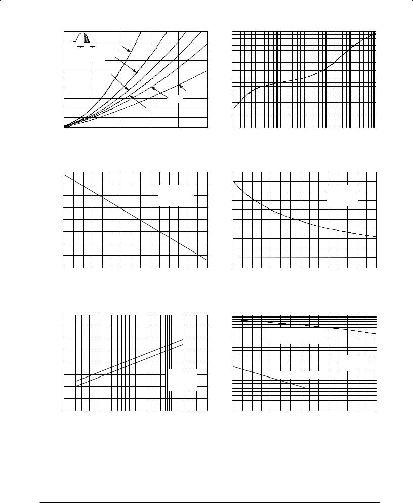
Figure 16. Exponential Static dv/dt versus Peak |
Figure 17. Exponential Static dv/dt versus |
Voltage and Gate-Cathode Termination Resistance |
Gate-Cathode Capacitance and Resistance |
|
10000 |
|
|
|
|
|
|
1000 |
|
|
|
|
|
μS) |
500 |
|
|
|
|
|
|
|
|
|
|
||
(V/ |
100 |
|
|
|
|
|
dv/dt |
50 |
|
|
|
|
|
STATIC |
|
|
|
|
||
10 |
|
|
IGT = 70 μA |
|
||
IGT = 5 |
μA |
IGT = 35 |
μA |
|||
|
|
|||||
|
|
|
|
|||
|
5.0 |
|
|
|
|
|
|
1.0 |
|
IGT = 15 μA |
|
|
|
|
100 |
1000 |
10,000 |
100,000 |
||
|
10 |
|||||
|
|
GATE-CATHODE RESISTANCE (OHMS) |
|
|||
Figure 18. Exponential Static dv/dt versus
Gate-Cathode Termination Resistance and
Product Trigger Current Sensitivity
Motorola Thyristor Device Data |
5 |

MCR08BT1 Series
PACKAGE DIMENSIONS
A
F
|
4 |
STYLE 10: |
|
|
|
PIN 1. |
CATHODE |
||
S |
B |
|||
2. |
ANODE |
|||
1 |
2 3 |
3. |
GATE |
|
|
|
4. |
ANODE |
|
|
D |
|
|
|
L |
G |
|
|
|
|
|
J |
||
|
|
|
||
|
C |
|
|
|
0.08 (0003) |
|
M |
|
|
H |
|
K |
||
|
|
|||
|
|
|
NOTES:
2DIMENSIONING AND TOLERANCING PER ANSI Y14.5M, 1982.
3CONTROLLING DIMENSION: INCH.
|
INCHES |
MILLIMETERS |
||
DIM |
MIN |
MAX |
MIN |
MAX |
A |
0.249 |
0.263 |
6.30 |
6.70 |
B |
0.130 |
0.145 |
3.30 |
3.70 |
C |
0.060 |
0.068 |
1.50 |
1.75 |
D |
0.024 |
0.035 |
0.60 |
0.89 |
F |
0.115 |
0.126 |
2.90 |
3.20 |
G |
0.087 |
0.094 |
2.20 |
2.40 |
H |
0.0008 |
0.0040 |
0.020 |
0.100 |
J |
0.009 |
0.014 |
0.24 |
0.35 |
K |
0.060 |
0.078 |
1.50 |
2.00 |
L |
0.033 |
0.041 |
0.85 |
1.05 |
M |
0 |
10 |
0 |
10 |
S |
0.264 |
0.287 |
6.70 |
7.30 |
CASE 318E-04 (SOT±223)
Motorola reserves the right to make changes without further notice to any products herein. Motorola makes no warranty, representation or guarantee regarding the suitability of its products for any particular purpose, nor does Motorola assume any liability arising out of the application or use of any product or circuit, and specifically disclaims any and all liability, including without limitation consequential or incidental damages. ªTypicalº parameters can and do vary in different applications. All operating parameters, including ªTypicalsº must be validated for each customer application by customer's technical experts. Motorola does not convey any license under its patent rights nor the rights of others. Motorola products are not designed, intended, or authorized for use as components in systems intended for surgical implant into the body, or other applications intended to support or sustain life, or for any other application in which the failure of the Motorola product could create a situation where personal injury or death may occur. Should Buyer purchase or use Motorola products for any such unintended or unauthorized application, Buyer shall indemnify and hold Motorola and its officers, employees, subsidiaries, affiliates, and distributors harmless against all claims, costs, damages, and expenses, and reasonable attorney fees arising out of, directly or indirectly, any claim of personal injury or death associated with such unintended or unauthorized use, even if such claim alleges that Motorola was negligent regarding the design or manufacture of the part. Motorola and  are registered trademarks of Motorola, Inc. Motorola, Inc. is an Equal Opportunity/Affirmative Action Employer.
Literature Distribution Centers:
USA: Motorola Literature Distribution; P.O. Box 20912; Phoenix, Arizona 85036.
EUROPE: Motorola Ltd.; European Literature Centre; 88 Tanners Drive, Blakelands, Milton Keynes, MK14 5BP, England. JAPAN: Nippon Motorola Ltd.; 4-32-1, Nishi-Gotanda, Shinagawa-ku, Tokyo 141, Japan.
ASIA PACIFIC: Motorola Semiconductors H.K. Ltd.; Silicon Harbour Center, No. 2 Dai King Street, Tai Po Industrial Estate, Tai Po, N.T., Hong Kong.
◊ |
MCR08BT1/D |
*MCR08BT1/D*