

MOTOROLA
SEMICONDUCTOR TECHNICAL DATA
Order this document by MOC2A60±10/D
POWER OPTO Isolator
2 Amp Zero±Cross Triac Output
This device consists of a gallium arsenide infrared emitting diode optically coupled to a zero±cross triac driver circuit and a power triac. It is capable of driving a load of up to 2 amps (rms) directly, on line voltages from 20 to 280 volts ac (rms).
•Provides Normally Open Solid State AC Output with 2 Amp Rating
•70 Amp Single Cycle Surge Capability
•Zero±Voltage Turn±on and Zero±Current Turn±off
•High Input±Output Isolation of 3750 vac (rms)
•Static dv/dt Rating of 400 Volts/μs Guaranteed
•2 Amp Pilot Duty Rating Per UL508 W117 (Overload Test) and W118 (Endurance Test)  [File No. 129224]
•CSA Approved [File No. CA77170±1].
•SEMKO Approved Certificate #9507228
•Exceeds NEMA 2±230 and IEEE472 Noise Immunity Test Requirements (See Fig.14)
DEVICE RATINGS (TA = 25°C unless otherwise noted)
Rating |
Symbol |
Value |
Unit |
|
|
|
|
INPUT LED |
|
|
|
|
|
|
|
Forward Current Ð Maximum Continuous |
IF |
50 |
mA |
Forward Current Ð Maximum Peak |
IF(pk) |
1.0 |
A |
(PW = 100ms, 120 pps) |
|
|
|
Reverse Voltage Ð Maximum |
VR |
6.0 |
V |
OUTPUT TRIAC |
|
|
|
|
|
|
|
Output Terminal Voltage Ð Maximum Transient (1) |
V |
600 |
V(pk) |
|
DRM |
|
|
Operating Voltage Range Ð Maximum Continuous |
VT |
20 to 280 |
Vac(rms) |
(f = 47 ± 63 Hz) |
|
|
|
|
|
|
|
On±State Current Range |
IT(rms) |
0.03 to 2.0 |
A |
(Free Air, Power Factor ≥ 0.3) |
|
|
|
Non±Repetitive Single Cycle Surge Current Ð |
ITSM |
70 |
A |
Maximum Peak (t = 16.7 ms) |
|
|
|
|
|
|
|
Main Terminal Fusing Current (t = 8.3 ms) |
I2T |
26 |
A2sec |
Load Power Factor Range |
PF |
0.3 to 1.0 |
Ð |
|
|
|
|
Junction Temperature Range |
TJ |
± 40 to 125 |
°C |
TOTAL DEVICE |
|
|
|
|
|
|
|
Input±Output Isolation Voltage Ð Maximum (2) |
VISO |
3750 |
Vac(rms) |
47 ± 63 Hz, 1 sec Duration |
|
|
|
|
|
|
|
Thermal Resistance Ð Power Triac Junction to Case |
RqJC |
8.0 |
°C/W |
(See Fig. 15) |
|
|
|
|
|
|
|
Ambient Operating Temperature Range |
Toper |
± 40 to +100 |
°C |
Storage Temperature Range |
Tstg |
± 40 to +150 |
°C |
Lead Soldering Temperature Ð Maximum |
TL |
260 |
°C |
(1/16″ from Case, 10 sec Duration) |
|
|
|
1.Test voltages must be applied within dv/dt rating.
2.Input±Output isolation voltage, VISO, is an internal device dielectric breakdown rating. For this
2.test, pins 2, 3 and the heat tab are common, and pins 7 and 9 are common.
MOC2A60-10
MOC2A60-5*
*Motorola Preferred Device
OPTOISOLATOR
2 AMP ZERO CROSS
TRIAC OUTPUT
600 VOLTS
7 9 |
CASE 417±02 |
Style 2 |
2 3 PLASTIC PACKAGE
CASE 417A±02
Style 1
PLASTIC PACKAGE
CASE 417B±01
Style 1
PLASTIC PACKAGE
DEVICE SCHEMATIC
7
3 

2ZVA 
*
9
* Zero Voltage Activate Circuit
1, 4, 5, 6, 8. NO PIN
2.LED CATHODE
3.LED ANODE
7. MAIN TERMINAL 2
9. MAIN TERMINAL 1
POWER OPTO is a trademark of Motorola, Inc.
Preferred devices are Motorola recommended choices for future use and best overall value.
REV 2
Motorola, Inc. 1995

MOC2A60-10 MOC2A60-5
ELECTRICAL CHARACTERISTICS (TA = 25°C unless otherwise noted)
Characteristic |
|
Symbol |
Min |
Typ |
Max |
Unit |
|
|
|
|
|
|
|
INPUT LED |
|
|
|
|
|
|
|
|
|
|
|
|
|
Forward Voltage (IF = 10 mA) |
|
VF |
1.00 |
1.17 |
1.50 |
V |
Reverse Leakage Current (VR = 6.0 V) |
|
IR |
Ð |
1.0 |
100 |
μA |
Capacitance |
|
C |
Ð |
18 |
Ð |
pF |
|
|
|
|
|
|
|
OUTPUT TRIAC |
|
|
|
|
|
|
|
|
|
|
|
|
|
Off±State Leakage, Either Direction |
|
IDRM |
Ð |
0.25 |
10 |
μA |
(IF = 0, VDRM = 600 V) |
|
|
|
|
|
|
Critical Rate of Rise of Off±State Voltage (Static) |
|
dv/dt(s) |
400 |
Ð |
Ð |
V/μs |
V = 400 vac(pk)) (1)(2) |
|
|
|
|
|
|
in |
|
|
|
|
|
|
Holding Current, Either Direction (IF = 0, VD = 12 V, IT = 200 mA) |
IH |
Ð |
10 |
Ð |
mA |
|
COUPLED |
|
|
|
|
|
|
|
|
|
|
|
|
|
LED Trigger Current Required to Latch Output |
MOC2A60±10 |
IFT(on) |
Ð |
7.0 |
10 |
mA |
Either Direction (Main Terminal Voltage = 2.0 V)(3)(4) |
MOC2A60±5 |
IFT(on) |
Ð |
3.5 |
5.0 |
mA |
On±State Voltage, Either Direction (IF = Rated IFT(on), ITM = 2.0 A) |
VTM |
Ð |
0.96 |
1.3 |
V |
|
Inhibit Voltage, Either Direction (IF = Rated IFT(on))(5) |
|
VINH |
Ð |
8.0 |
10 |
V |
(Main Terminal Voltage above which device will not trigger) |
|
|
|
|
|
|
|
|
|
|
|
|
|
Commutating dv/dt (Rated VDRM, IT = 30 mA ± 2.0 A(rms), |
dv/dt (c) |
5.0 |
Ð |
Ð |
V/μS |
|
T = ± 40 ± 100°C, f = 60 Hz)(2) |
|
|
|
|
|
|
A |
|
|
|
|
|
|
Common±mode Input±Output dv/dt(2) |
|
dv/dt(cm) |
Ð |
40,000 |
Ð |
V/μS |
Input±Output Capacitance (V = 0, f = 1.0 MHz) |
|
CISO |
Ð |
1.3 |
Ð |
pF |
Isolation Resistance (VI±O = 500 V) |
|
RISO |
1012 |
1014 |
Ð |
Ω |
1.Per EIA/NARM standard RS±443, with VP = 200 V, which is the instantaneous peak of the maximum operating voltage.
2.Additional dv/dt information, including test methods, can be found in Motorola applications note AN1048/D, Figure 43.
3.All devices are guaranteed to trigger at an IF value less than or equal to the max IFT. Therefore, the recommended operating IF lies between
3.the device's maximum IFT(on) limit and the Maximum Rating of 50 mA.
4.Current±limiting resistor required in series with LED.
5.Also known as ªZero Voltage Turn±On.º
|
|
|
|
|
|
|
TYPICAL CHARACTERISTICS |
|
|
||||
|
100 |
|
|
|
|
|
|
|
|
2.00 |
PULSE ONLY |
|
|
|
|
|
|
|
|
|
|
|
|
|
|
|
|
(mA)CURRENT |
|
|
|
|
|
|
|
|
|
1.80 |
PULSE OR DC |
|
|
80 |
|
|
|
|
|
|
|
(V)VOLTAGE |
|
|
|
||
|
|
|
|
|
|
|
|
|
|
|
|||
|
|
|
|
|
|
|
|
|
|
|
|
|
|
|
|
|
|
|
|
|
|
|
|
1.60 |
|
|
|
|
60 |
|
|
|
|
|
|
|
|
|
|
|
|
LED |
|
|
|
|
|
|
|
|
FORWARD |
1.40 |
|
|
|
40 |
|
|
|
|
|
|
|
|
TA = ± 40°C |
|
|
||
FORWARD, |
|
|
|
|
|
|
|
|
|
|
|
||
20 |
|
|
|
|
|
|
|
V |
1.00 |
|
|
||
|
|
|
|
|
|
|
25°C |
|
|
||||
|
|
|
|
|
|
|
|
|
|
1.20 |
|
|
|
|
|
|
|
|
|
|
|
|
, |
|
|
|
|
|
|
|
|
|
|
|
|
|
F |
|
|
|
|
F |
|
|
|
|
|
|
|
|
|
|
|
|
|
I |
|
|
|
|
|
|
|
|
|
|
100°C |
|
|
|
0 |
|
|
|
|
|
|
|
|
0.80 |
|
|
|
|
|
|
|
|
|
|
|
|
|
|
|
||
|
±40 |
±20 |
0 |
20 |
40 |
60 |
80 |
100 |
120 |
1 |
10 |
100 |
1000 |
|
|
|
TA, AMBIENT TEMPERATURE (°C) |
|
|
|
IF, FORWARD CURRENT (mA) |
|
|||||
Figure 1. Maximum Allowable Forward LED |
Figure 2. LED Forward Voltage |
Current versus Ambient Temperature |
versus LED Forward Current |
2 |
Motorola Optoelectronics Device Data |

|
1.60 |
|
|
|
|
|
|
|
|
CURRENT |
1.50 |
|
|
|
|
|
|
|
|
1.40 |
|
|
|
|
WORST CASE UNIT |
|
|
||
|
|
|
|
|
|
|
|||
|
|
|
|
|
NORMALIZED TO |
|
|
||
TRIGGER |
1.30 |
|
|
|
|
|
|
||
|
|
|
|
TA = 25°C |
|
|
|||
|
|
|
|
|
|
|
|||
1.20 |
|
|
|
|
|
|
|
|
|
|
|
|
|
|
|
|
|
|
|
, FORWARD |
1.10 |
|
|
|
|
|
|
|
|
1.00 |
|
|
|
|
|
|
|
|
|
|
|
|
|
|
|
|
|
|
|
IFT |
0.90 |
|
|
|
|
|
|
|
|
I |
|
|
|
|
|
|
|
|
|
|
0.80 |
|
|
|
|
|
|
|
|
|
±40 |
±20 |
0 |
20 |
40 |
60 |
80 |
100 |
120 |
|
|
|
TA, AMBIENT TEMPERATURE (°C) |
|
|
||||
|
|
|
MOC2A60-10 |
MOC2A60-5 |
|||||
|
2.4 |
|
|
|
|
|
|
|
|
|
2.0 |
|
|
|
|
|
|
|
|
(A) |
|
|
|
|
|
|
|
|
|
CURRENT |
1.6 |
|
|
|
|
|
|
|
|
1.2 |
|
|
|
|
|
|
|
|
|
, TERMINAL |
0.8 |
|
|
|
|
|
|
|
|
|
|
|
|
|
|
|
|
|
|
T |
0.4 |
|
|
|
|
|
|
|
|
I |
|
|
|
|
|
|
|
|
|
|
|
|
|
|
|
|
|
|
|
|
0.0 |
|
|
|
|
|
|
|
|
|
±40 |
±20 |
0 |
20 |
40 |
60 |
80 |
100 |
120 |
|
|
|
TA, AMBIENT TEMPERATURE (°C) |
|
|
||||
Figure 3. Forward LED Trigger Current |
Figure 4. Maximum Allowable On±State RMS Output |
versus Ambient Temperature |
Current (Free Air) versus Ambient Temperature |
VTM, MAIN TERMINAL VOLTAGE (V)
2.20 |
|
|
|
|
|
|
|
|
|
|
|
|
|
|
|
|
|
|
|
|
|
|
|
|
|
|
|
|
|
|
|
|
|
|
|
|
|
|
|
PULSE ONLY |
|
|
|
|
|
|
|
|
|
2.00 |
|
|
|
|
|
|
|
|
|
|
|
|
|
|
|
|
|
|
|
|
|
|
|
|
|
|
|
|
|
|
|
|
|
|
|
|
|
|
|
PULSE OR DC |
|
|
|
|
|
|
|
||
1.80 |
|
|
|
|
|
|
|
|
|
|
|
|
|
|
|
|
|
|
|
|
|
|
||
|
|
|
|
|
|
|
|
|
|
|
|
|
|
|
|
|
|
|
|
|
|
|||
|
|
|
|
|
|
|
|
|
|
|
|
|
|
|
|
|
|
|
|
|
|
|
|
|
|
|
|
|
|
|
|
|
|
|
|
|
|
|
|
|
|
|
|
|
|
|
|
|
|
1.60 |
|
|
|
|
|
|
|
|
|
|
|
|
|
|
|
|
|
|
|
|
|
|
|
|
|
|
|
|
|
|
|
|
|
|
|
|
|
|
|
|
|
|
|
|
|
|
|
|
|
1.40 |
|
|
|
|
|
|
|
|
|
|
|
|
|
|
|
|
|
|
|
|
|
|
|
|
|
|
|
|
|
|
|
|
|
|
|
|
|
|
|
|
|
|
|
|
|
|
|
|
|
1.20 |
|
|
|
|
|
|
|
|
|
|
|
|
|
|
|
|
|
|
|
|
|
|
|
|
|
|
|
|
|
|
|
|
|
|
|
|
|
|
|
|
|
|
|
|
|
|
|
|
|
1.00 |
|
|
|
|
|
|
|
|
|
|
|
|
|
|
|
|
|
|
|
|
|
|
|
|
|
|
|
|
|
|
|
TJ = 25 |
°C |
|
|
|
|
|
|
|
|
|
|
|
|
|
|
|
|
0.80 |
|
|
|
|
|
|
|
|
|
|
|
|
|
|
|
|
|
|
|
|
|
|
||
|
|
|
|
|
|
|
|
100° |
C |
|
|
|
|
|
|
|
|
|
|
|
|
|
||
0.60 |
|
|
|
|
|
|
|
|
|
|
|
|
|
|
|
|
|
|
|
|
|
|||
|
|
|
|
|
|
|
|
|
|
|
|
|
|
|
|
|
|
|
|
|
|
|
|
|
0.03 0.1 1.0
ITM, INSTANTANEOUS ON±STATE CURRENT (A)
Figure 5. On±State Voltage Drop versus
Output Terminal Current
(WATTS) |
2.5 |
|
|
||
2.0 |
|
|
DISSIPATION |
|
|
1.5 |
|
|
|
|
|
POWER |
1.0 |
|
0.5 |
|
|
PD, |
|
|
|
|
|
|
0.0 |
|
|
|
|
|
0.01 |
|
MAXIMUM
MEAN
0.1 1.0 10 IT, MAIN TERMINAL CURRENT (A)
Figure 6. Power Dissipation versus Main Terminal Current
|
120 |
|
|
|
LEAKAGE CURRENT (NORMALIZED) |
100 |
|
|
|
|
|
|
|
|
JUNCTION TEMPERATURE (°C) |
100 |
TA = 25°C |
|
|
|
|
|
|
|
|
|
|
|
|
|
|
|
|
NORMALIZED TO |
|
|
|
|
|
|
||||
|
|
|
|
10 |
|
|
|
|
|
|
||||
|
|
|
|
|
TA = 25°C |
|
|
|
|
|
|
|||
80 |
|
|
|
|
|
|
|
|
|
|
|
|||
|
|
|
|
|
|
|
|
|
|
|
|
|||
60 |
|
|
|
1.0 |
|
|
|
|
|
|
|
|
||
40 |
|
|
|
|
|
|
|
|
|
|
|
|
||
|
|
|
|
0.1 |
|
|
|
|
|
|
|
|
||
20 |
|
|
|
|
|
|
|
|
|
|
|
|
||
, |
|
|
|
, |
|
|
|
|
|
|
|
|
|
|
J |
|
|
|
|
|
|
|
|
|
|
|
|
||
T |
|
|
|
|
DRM |
|
|
|
|
|
|
|
|
|
|
0 |
|
|
|
I |
0.01 |
|
|
|
|
|
|
|
|
|
|
|
10 |
|
|
|
|
|
|
|
|
|
||
|
0.01 |
0.1 |
1 |
|
± 40 |
± 20 |
0 |
20 |
40 |
60 |
80 |
100 |
120 |
|
|
|
IT, MAIN TERMINAL CURRENT (A) |
|
|
|
|
TA, AMBIENT TEMPERATURE (°C) |
|
|
|||||
Figure 7. Junction Temperature versus Main |
Figure 8. Leakage with LED Off versus |
Terminal RMS Current (Free Air) |
Ambient Temperature |
Motorola Optoelectronics Device Data |
3 |

MOC2A60-10 MOC2A60-5 |
|
|
|
|
|
|
|
|
|
|
|
||||||
|
2.00 |
|
|
|
|
|
|
|
1000 |
|
|
|
|
|
|
|
|
|
1.80 |
|
|
|
|
|
|
|
|
|
|
|
|
|
STATIC |
|
|
|
1.60 |
|
|
|
|
|
|
|
|
|
|
|
|
|
|
|
|
(mA) |
|
|
|
NORMALIZED TO |
|
|
|
|
|
|
|
|
|
|
|
||
1.40 |
|
|
|
|
|
|
|
|
|
|
|
|
|
|
|||
|
|
|
TA = 25°C |
|
|
100 |
|
|
|
|
|
|
|
|
|||
CURRENT |
|
|
|
|
|
|
|
|
|
|
|
|
|
||||
1.20 |
|
|
|
|
|
|
|
|
|
|
|
|
|
||||
|
|
|
|
|
|
(V/ μS) |
|
|
|
|
|
|
|
|
|
||
1.00 |
|
|
|
|
|
|
|
|
|
|
|
|
|
|
|
||
|
|
|
|
|
|
|
|
|
|
|
|
|
|
|
|
||
HOLDING |
0.80 |
|
|
|
|
|
|
dv/dt |
|
|
|
|
|
|
COMMUTATING |
|
|
0.60 |
|
|
|
|
|
|
10 |
|
|
|
|
|
|
||||
|
|
|
|
|
|
|
|
|
|
|
|
|
|
|
|||
|
|
|
|
|
|
|
|
|
|
|
|
|
|
|
|
||
, |
|
|
|
|
|
|
|
|
|
|
|
|
|
|
|
|
|
H |
0.40 |
|
|
|
|
|
|
|
|
|
|
|
|
|
|
|
|
I |
|
|
|
|
|
|
|
|
|
|
|
|
|
|
|
|
|
|
0.20 |
|
|
|
|
|
|
|
|
IT = 30 mA ± 2A(RMS) |
|
|
|
|
|
|
|
|
0.00 |
|
|
|
|
|
|
|
0 |
F = 60 Hz |
|
|
|
|
|
|
|
|
|
|
|
|
|
|
|
|
|
|
40 |
|
|
|
|
||
|
± 40 |
± 20 |
0 |
+ 25 |
+ 40 |
+ 60 |
+ 80 |
+ 100 |
± 40 |
± 20 |
0 |
20 |
60 |
80 |
100 |
120 |
|
|
|
|
TA, AMBIENT TEMPERATURE (°C) |
|
|
|
|
TA, AMBIENT TEMPERATURE (°C) |
|
|
|||||||
Figure 9. Holding Current versus |
Figure 10. dv/dt versus Ambient Temperature |
Ambient Temperature |
|
LED INPUT
VOLTAGE
PIN 7 TO 9
TURN ON
POINTS
Figure 11. Operating Waveforms
MOC2A60
VCC
R2
MOV
R1 |
C1 |
|
|
|
ZVA |
|
* |
LOAD
*ZERO VOLTAGE ACTIVATE CIRCUIT
Figure 12. Typical Application Circuit
Select the value of R1 according to the following formulas:
[1]R1 = (VCC ± VF) / Max. IFT (on) per spec.
[2]R1 = (VCC ± VF) / 0.050
Typical values for C1 and R2 are 0.01 μF and 39 Ω, respectively. You may adjust these values for specific applications. The maximum recommended value of C1 is 0.022 μF. See application note AN1048 for additional information on component values.
The MOV may or may not be needed depending upon the characteristics of the applied ac line voltage. For applications where line spikes may exceed the 600 V rating of the MOC2A60, an MOV is required.
4 |
Motorola Optoelectronics Device Data |

MOC2A60-10 MOC2A60-5
Use care to maintain the minimum spacings as shown. Safety and regulatory requirements dictate a minimum of 8.0 mm between the closest points between input and output conducting paths, Pins 3 and 7. Also, 0.070 inches distance is required between the two output Pins, 7 and 9.
Keep pad sizes on Pins 7 and 9 as large as possible for optimal performance.
0.070″ MIN
0.315″ MIN [8 MM MIN]
Figure 13. PC Board Layout Recommendations
Each device, when installed in the circuit shown in Figure 14, shall be capable of passing the following conducted noise tests:
•IEEE 472 (2.5 KV)
•Lamp Dimmer (NEMA Part DC33, w 3.4.2.1)
•NEMA ICS 2±230.45 Showering Arc
•MIL±STD±461A CS01, CS02 and CS06
DEVICE UNDER TEST |
NOISE |
|||
|
|
|
|
|
2 |
3 |
7 |
9 |
SOURCE |
|
||||
|
|
|
10W |
MOV |
|
|
|
|
150V |
IF = RATED IF |
|
0.022mF |
Z LOAD |
|
|
|
|
|
|
AC
SUPPLY
Figure 14. Test Circuit for Conducted Noise Tests
|
|
NO ADDITIONAL HEATSINK |
|
|
|
|
TJ |
|
TC |
TA |
|
JUNCTION |
|
RqJC |
RqCA |
|
AMBIENT AIR |
TEMPERATURE OF |
HEAT FLOW |
|
|
||
MOC2A60 . . . { |
|
WITH ADDITIONAL HEATSINK |
} |
TEMPERATURE |
|
|
|
||||
OUTPUT CHIP |
TJ |
TC |
TS |
TA |
|
|
|
||||
RqJC
Terms in the model signify:
TA = Ambient temperature TS = Optional additional TS = heat sink temperature TC = Case temperature
TJ = Junction temperature PD = Power dissipation
RqCS RqSA
RθSA = Thermal resistance, heat sink to ambient RθCA = Thermal resistance, case to ambient RθCS = Thermal resistance, heat sink to case RθJC = Thermal resistance, junction to case
Values for thermal resistance components are: RθCA = 36°C/W/in maximum Values for thermal resistance components are: RθJC = 8.0°C/W maximum
The design of any additional heatsink will determine the values of RθSA and RθCS.
TC ± TA = PD (RθCA)
TC ± TA = PD (RθJC) + RθSA), where PD = Power Dissipation in Watts.
Figure 15. Approximate Thermal Circuit Model
Thermal measurements of RθJC are referenced to the point on the heat tab indicated with an `X'. Measurements should be taken with device orientated along its vertical axis.
Motorola Optoelectronics Device Data |
5 |

MOC2A60-10 MOC2A60-5
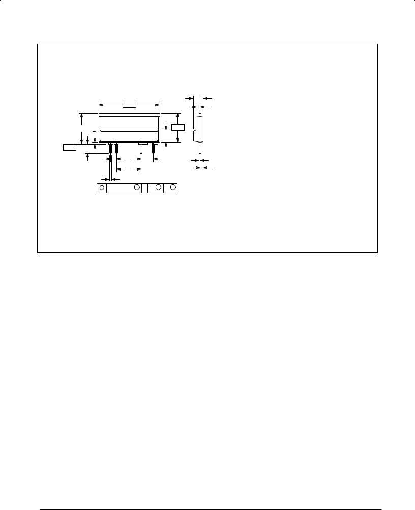
PACKAGE DIMENSIONS
|
|
|
|
C |
|
|
±A± |
|
E |
S |
|
|
|
±B± |
P |
|
|
|
|
2 3 |
7 |
9 |
N |
|
|
|
|
|
±T±
SEATING
PLANE K
V |
L |
J |
|
|
|
|
G |
H |
|
D 4 PL |
|
|
0.13 (0.005) M T A M |
B M |
CASE 417±02
PLASTIC
STANDARD HEAT TAB
ISSUE C
NOTES:
1.DIMENSIONING AND TOLERANCING PER ANSI Y14.5M, 1982.
2.CONTROLLING DIMENSION: INCH.
|
INCHES |
MILLIMETERS |
||
DIM |
MIN |
MAX |
MIN |
MAX |
A |
0.965 |
1.005 |
24.51 |
25.53 |
B |
0.416 |
0.436 |
10.57 |
11.07 |
C |
0.170 |
0.190 |
4.32 |
4.83 |
D |
0.025 |
0.035 |
0.64 |
0.89 |
E |
0.040 |
0.060 |
1.02 |
1.52 |
G |
0.400 BSC |
10.16 BSC |
||
H |
0.040 |
0.060 |
1.02 |
1.52 |
J |
0.012 |
0.018 |
0.30 |
0.46 |
K |
0.134 |
0.154 |
3.40 |
3.91 |
L |
0.200 BSC |
5.08 BSC |
||
N |
0.190 |
0.210 |
4.83 |
5.33 |
P |
0.023 |
0.043 |
0.58 |
1.09 |
S |
0.695 |
0.715 |
17.65 |
18.16 |
V |
0.100 BSC |
2.54 BSC |
||
STYLE 2: |
|
PIN 2. |
LED CATHODE |
3. |
LED ANODE |
7. |
TRIAC MT |
9. |
TRIAC MT |
ORDER ªFº SUFFIX |
|
|
|
|
|
|
||
HEAT TAB OPTION |
|
|
|
|
|
|
||
(EX: MOC2A60±10F) |
|
|
|
|
|
|
||
|
|
|
|
|
±A± |
|
|
C |
Z RADIUS |
|
|
|
U |
|
W |
E |
|
|
|
|
Y |
|
|
Q |
||
|
|
|
|
|
|
|
||
|
|
|
|
|
|
|
|
|
|
|
|
|
|
|
|
|
X |
S |
R |
|
|
|
|
|
|
|
|
|
|
|
|
|
|
|
|
|
|
P |
|
|
|
|
|
±B± |
|
|
2 |
3 |
7 |
9 |
N |
|
|
|
|
|
|
|||||
±T± |
|
|
|
|
|
|
|
|
SEATING |
|
K |
|
|
|
|
|
J |
PLANE |
|
V |
|
G |
L |
|
||
|
|
|
|
|
H |
|||
|
|
|
|
|
D 4 PL |
|
|
|
|
|
|
|
|
|
|
|
|
NOTES:
1.DIMENSIONING AND TOLERANCING PER ANSI Y14.5M, 1982.
2.CONTROLLING DIMENSION: INCH.
|
INCHES |
MILLIMETERS |
||
DIM |
MIN |
MAX |
MIN |
MAX |
A |
0.965 |
1.005 |
24.51 |
25.53 |
B |
0.416 |
0.436 |
10.57 |
11.07 |
C |
0.170 |
0.190 |
4.32 |
4.83 |
D |
0.025 |
0.035 |
0.64 |
0.89 |
E |
0.040 |
0.060 |
1.02 |
1.52 |
G |
0.400 BSC |
10.16 BSC |
||
H |
0.040 |
0.060 |
1.02 |
1.52 |
J |
0.012 |
0.018 |
0.30 |
0.46 |
K |
0.134 |
0.154 |
3.40 |
3.91 |
L |
0.200 BSC |
5.08 BSC |
||
N |
0.190 |
0.210 |
4.83 |
5.33 |
P |
0.023 |
0.043 |
0.58 |
1.09 |
Q |
0.057 |
0.067 |
1.45 |
1.70 |
R |
0.734 |
0.754 |
18.64 |
19.15 |
S |
0.840 |
0.870 |
21.34 |
22.10 |
U |
0.593 |
0.613 |
15.06 |
15.57 |
V |
0.100 BSC |
2.54 BSC |
||
W |
0.074 |
0.094 |
1.88 |
2.39 |
X |
0.265 |
0.295 |
6.73 |
7.49 |
Y |
0.079 |
0.089 |
2.01 |
2.26 |
Z |
0.026 |
0.036 |
0.66 |
0.91 |
0.13 (0.005) M T A M B M
STYLE 1:
PIN 2. LED CATHODE
3. LED ANODE
7. TRIAC MT
CASE 417A±02 9. TRIAC MT
PLASTIC
FLUSH MOUNT HEAT TAB
ISSUE A
6 |
Motorola Optoelectronics Device Data |
MOC2A60-10 MOC2A60-5
PACKAGE DIMENSIONS Ð CONTINUED
ORDER ªCº SUFFIX HEAT TAB OPTION (EX: MOC2A60±10C)
|
|
±A± |
|
|
C |
|
|
|
|
E |
|
|
|
|
|
|
|
|
S |
P |
|
|
±B± |
|
|
|
|
N |
|
|
|
2 3 |
7 |
9 |
|
±T± |
|
K |
|
|
|
SEATING |
|
|
|
|
|
|
|
|
|
|
|
PLANE |
|
V |
|
L |
J |
|
|
|
|||
|
|
G |
|
|
H |
|
|
D 4 PL |
|
|
|
|
|
0.13 (0.005) M |
T |
A M |
B M |
CASE 417B±01
PLASTIC
CUT HEAT TAB
ISSUE O
NOTES:
1.DIMENSIONING AND TOLERANCING PER ANSI Y14.5M, 1982.
2.CONTROLLING DIMENSION: INCH.
|
INCHES |
MILLIMETERS |
||
DIM |
MIN |
MAX |
MIN |
MAX |
A |
0.965 |
1.005 |
24.51 |
25.53 |
B |
0.416 |
0.436 |
10.57 |
11.07 |
C |
0.170 |
0.190 |
4.32 |
4.83 |
D |
0.025 |
0.035 |
0.64 |
0.89 |
E |
0.040 |
0.060 |
1.02 |
1.52 |
G |
0.400 BSC |
10.16 BSC |
||
H |
0.040 |
0.060 |
1.02 |
1.52 |
J |
0.012 |
0.060 |
0.30 |
0.46 |
K |
0.134 |
0.154 |
3.40 |
3.91 |
L |
0.200 BSC |
5.08 BSC |
||
N |
0.190 |
0.210 |
4.83 |
5.33 |
P |
0.023 |
0.043 |
0.58 |
1.09 |
S |
0.439 |
0.529 |
11.15 |
13.44 |
V |
0.100 BSC |
2.54 BSC |
||
STYLE 1: |
|
PIN 2. |
LED CATHODE |
3. |
LED ANODE |
7. |
TRIAC MT |
9. |
TRIAC MT |
Motorola Optoelectronics Device Data |
7 |

MOC2A60-10 MOC2A60-5
Motorola reserves the right to make changes without further notice to any products herein. Motorola makes no warranty, representation or guarantee regarding the suitability of its products for any particular purpose, nor does Motorola assume any liability arising out of the application or use of any product or circuit, and specifically disclaims any and all liability, including without limitation consequential or incidental damages. ªTypicalº parameters can and do vary in different applications. All operating parameters, including ªTypicalsº must be validated for each customer application by customer's technical experts. Motorola does not convey any license under its patent rights nor the rights of others. Motorola products are not designed, intended, or authorized for use as components in systems intended for surgical implant into the body, or other applications intended to support or sustain life, or for any other application in which the failure of the Motorola product could create a situation where personal injury or death may occur. Should Buyer purchase or use Motorola products for any such unintended or unauthorized application, Buyer shall indemnify and hold Motorola and its officers, employees, subsidiaries, affiliates, and distributors harmless against all claims, costs, damages, and expenses, and reasonable attorney fees arising out of, directly or indirectly, any claim of personal injury or death associated with such unintended or unauthorized use, even if such claim alleges that Motorola was negligent regarding the design or manufacture of the part. Motorola and  are registered trademarks of Motorola, Inc. Motorola, Inc. is an Equal Opportunity/Affirmative Action Employer.
How to reach us: |
|
USA / EUROPE: Motorola Literature Distribution; |
JAPAN: Nippon Motorola Ltd.; Tatsumi±SPD±JLDC, Toshikatsu Otsuki, |
P.O. Box 20912; Phoenix, Arizona 85036. 1±800±441±2447 |
6F Seibu±Butsuryu±Center, 3±14±2 Tatsumi Koto±Ku, Tokyo 135, Japan. 03±3521±8315 |
MFAX: RMFAX0@email.sps.mot.com ± TOUCHTONE (602) 244±6609 HONG KONG: Motorola Semiconductors H.K. Ltd.; 8B Tai Ping Industrial Park, |
|
INTERNET: http://Design±NET.com |
51 Ting Kok Road, Tai Po, N.T., Hong Kong. 852±26629298 |
◊ MOC2A60±10/D
*MOC2A60-10/D*