

MOTOROLA
SEMICONDUCTOR TECHNICAL DATA
Order this document by MRF166C/D
The RF MOSFET Line
RF Power
Field Effect Transistors
N±Channel Enhancement Mode MOSFETs
Designed primarily for wideband large±signal output and driver from 30±500 MHz.
•Low Crss Ð 4.5 pF @ V DS = 28 V
•MRF166C Ð Typical Performance at 400 MHz, 28 Vdc Output Power = 20 W
Gain = 17 dB Efficiency = 55%
•Replacement for Industry Standards such as MRF136, DV2820, BLF244, SD1902, and ST1001
•100% Tested for Load Mismatch at all Phase Angles with 30:1 VSWR
•Facilitates Manual Gain Control, ALC and Modulation Techniques
•Excellent Thermal Stability, Ideally Suited for Class A Operation
•Circuit board photomaster available upon request by
contacting RF Tactical Marketing in Phoenix, AZ. |
D |
G
 S
S
MAXIMUM RATINGS
MRF166C
20 W, 500 MHz
MOSFET
BROADBAND
RF POWER FETs
CASE 319±07, STYLE 3
Rating |
Symbol |
Value |
Unit |
|
|
|
|
Drain±Gate Voltage |
VDSS |
65 |
Vdc |
Drain±Gate Voltage |
VDGR |
65 |
Vdc |
(RGS = 1.0 MΩ) |
|
|
|
Gate±Source Voltage |
VGS |
± 40 |
Adc |
Drain Current Ð Continuous |
ID |
4.0 |
Adc |
Total Device Dissipation @ TC = 25°C |
PD |
70 |
Watts |
Derate Above 25°C |
|
0.4 |
W/°C |
|
|
|
|
Storage Temperature Range |
Tstg |
± 65 to 150 |
°C |
Operating Junction Temperature |
TJ |
200 |
°C |
THERMAL CHARACTERISTICS |
|
|
|
|
|
|
|
Characteristic |
Symbol |
Max |
Unit |
|
|
|
|
Thermal Resistance, Junction to Case |
RθJC |
2.5 |
°C/W |
NOTE Ð CAUTION Ð MOS devices are susceptible to damage from electrostatic charge. Reasonable precautions in handling and packaging MOS devices should be observed.
REV 7
Motorola, Inc. 1995

ELECTRICAL CHARACTERISTICS (TC = 25°C unless otherwise noted)
Characteristic |
Symbol |
Min |
Typ |
Max |
Unit |
|
|
|
|
|
|
OFF CHARACTERISTICS
Drain±Source Breakdown Voltage |
V(BR)DSS |
65 |
|
Ð |
Ð |
|
V |
(VGS = 0 V, ID = 5.0 mA) |
|
|
|
|
|
|
|
Zero Gate Voltage Drain Current |
IDSS |
Ð |
|
Ð |
1.0 |
|
mA |
(VDS = 28 V, VGS = 0 V) |
|
|
|
|
|
|
|
Gate±Source Leakage Current |
IGSS |
Ð |
|
Ð |
1.0 |
|
μA |
(VGS = 40 V, VDS = 0 V) |
|
|
|
|
|
|
|
ON CHARACTERISTICS |
|
|
|
|
|
|
|
|
|
|
|
|
|
|
|
Gate Threshold Voltage |
VGS(th) |
1.0 |
|
3.0 |
6.0 |
|
V |
(VDS = 10 V, ID = 25 mA) |
|
|
|
|
|
|
|
Forward Transconductance |
gfs |
600 |
|
800 |
Ð |
|
mhos |
(VDS = 10 V, ID = 1.5 A) |
|
|
|
|
|
|
|
DYNAMIC CHARACTERISTICS |
|
|
|
|
|
|
|
|
|
|
|
|
|
|
|
Input Capacitance |
Ciss |
Ð |
|
30 |
Ð |
|
pF |
(VDS = 28 V, VGS = 0 V, f = 1.0 MHz) |
|
|
|
|
|
|
|
Output Capacitance |
Coss |
Ð |
|
35 |
Ð |
|
pF |
(VDS = 28 V, VGS = 0 V, f = 1.0 MHz) |
|
|
|
|
|
|
|
Reverse Transfer Capacitance |
Crss |
Ð |
|
4.5 |
Ð |
|
pF |
(VDS = 28 V, VGS = 0 V, f = 1.0 MHz) |
|
|
|
|
|
|
|
FUNCTIONAL CHARACTERISTICS |
|
|
|
|
|
|
|
|
|
|
|
|
|
|
|
Noise Figure |
NF |
Ð |
|
2.5 |
Ð |
|
dB |
(VDD = 28 V, f = 30 MHz, IDQ = 50 mA) |
|
|
|
|
|
|
|
Common Source Power Gain |
Gps |
14 |
|
17 |
Ð |
|
dB |
(VDD = 28 V, Pout = 20 W, f = 400 MHz, IDQ = 100 mA) |
|
|
|
|
|
|
|
Drain Efficiency |
η |
50 |
|
55 |
Ð |
|
% |
(VDD = 28 V, Pout = 20 W, f = 400 MHz, IDQ = 100 mA) |
|
|
|
|
|
|
|
Electrical Ruggedness |
ψ |
|
|
|
|
|
|
(VDD = 28 V, Pout = 20 W, f = 400 MHz, IDQ = 100 mA, |
|
No Degradation in Output Power |
|
||||
Load VSWR 30:1 at All Phase Angles) |
|
|
|
|
|
|
|
|
|
|
|
|
|
|
|
MRF166C |
MOTOROLA RF DEVICE DATA |
2 |
|
|
|
|
|
|
|
|
|
|
|
|
|
|
|
|
|
|
|
|
|
|
|
|
|
|
|
|
|
|
|
|
|
|
|
|
|
|
|
|
|
|
|
|
|
|
|
|
|
|
|
|
|
|
|
R2 |
|
|
|
|
|
|
|
|
|
|
|
|
C10 |
RFC1 |
C11 |
|
|
|
|
|
|
|
|
|
|
|
|
VDD = 28 V |
||||||||||||||||||||||||||||||||||||||||||||||||||
|
|
|
|
|
|
|
|
|
|
|
|
|
|
|
|
|
|
|
|
|
|
|
|
|
|
|
|
|
|
|
|
|
|
|
|
|
|
|
|
|
|
|
|
|
|
|
|
|
|
|
|
|
|
|
|
|
|
|
|
|
|
|
|
|
|
|
|
|
|
|
|
|
|
|
|
|
|
|
|
|
|
|
|
|
|
|
|
|
|
|
|
|
|
|
|
|
|
|
|
|
|
|
|
|
+ |
|||||||||||||||||||||||||||
|
|
|
|
|
|
|
|
|
|
|
|
|
|
|
|
|
|
|
|
|
|
|
|
|
|
|
|
|
|
|
|
|
|
|
|
|
|
|
|
|
|
|
|
|
|
|
|
|
|
|
|
|
|
|
|
|
|
|
|
|
|
|
|
|
|
|
|
|
|
|
|
|
|
|
|
|
|
|
|
|
|
|
|
|
|
|
|
|
|
|
|
|
|
|
|
|
|
|
|
|
|
|
|
|
|
|
|
|
|
|
|
|
|
|
|
|
|
|
|
|
|
|
|
|
|
|
|
|
||||
|
|
|
|
|
|
R3 |
|
|
|
|
|
|
|
|
|
|
|
|
|
|
|
|
|
|
|
|
|
+ |
|
|
|
|
|
|
|
|
|
|
|
|
|
|
|
|
|
|
|
|
|
|
|
|
|
|
|
|
|
|
|
|
|
|
|
|
|
|
|
|
|
|
|
|
|
|
|
|
|
|
|
|
|
|
|
|
|
|
|
|
|
|
|
|
|
|
|
|
|
|
|
|
|
|
|
|
|
|
|
+ |
|
|
|
|
|
|
|
|
|
|
|
|
||||||||||||
|
|
|
|
|
|
|
|
|
|
|
C4 |
|
|
|
|
C13 |
|
|
|
|
|
|
|
|
|
|
|
|
|
|
|
|
|
|
|
|
|
|
|
|
|
C8 |
|
|
|
|
|
|
|
|
|
|
|
|
|
|
|
|
|
|
|
|
|
|
|
|
|
|
|
|
|
|
|
|
|
|
|
|
|
|
|
|
|
|
|
|
|
|
|
|
|
|
|
|
|
|
|
|
|
|
|
|
|
|
|
|
|
|
|
|
|
Vdc |
||||||||||||||||||||
|
|
|
|
|
|
|
|
|
|
|
|
|
|
|
|
|
|
|
|
|
|
|
|
|
|
|
|
|
|
|
|
|
|
|
|
|
|
|
|
|
|
|
|
|
|
|
|
|
|
|
|
|
|
|
|
|
|
|
|
|
|
|
|
|
|
|
|
|
|
|
|
|
|
|
|
|
|
|
|
|
|
|
|
|
|
|
|
|
|
|
|
|
|
|
|
|
|
|
|
|
|
|
|
|
|
|
|
|
||||||||||||||||||||||||
|
|
|
|
|
|
|
|
|
|
|
|
|
|
|
|
|
|
|
|
|
|
|
|
|
|
|
|
|
|
|
|
|
|
|
|
|
|
|
|
|
D1 |
|
|
|
|
|
|
|
|
|
|
|
|
|
|
|
|
|
|
|
|
|
|
|
|
|
|
|
|
|
|
|
|
|
|
|
|
|
|
|
|
|
|
|
|
|
|
|
|
|
|
|
|
|
|
|
|
|
|
C12 |
|
|
|
|
|
|
|
|
|
|
|
|
|
|
||||||||||||||||||
|
|
|
|
|
|
|
|
|
|
|
|
|
|
|
|
|
|
|
|
|
|
|
|
|
|
|
|
|
|
± |
|
|
|
|
|
|
|
|
|
|
|
|
|
|
|
|
|
|
|
|
|
|
|
|
|
|
|
|
|
|
|
|
|
|
|
|
|
|
|
|
|
|
|
|
|
|
|
|
|
|
|
|
|
|
|
|
|
|
|
|
|
|
|
|
|
|
|
|
|
|
|
|
|
|
|
|
|
± |
|
|
|
|
|
|
|
|
|
|
|
|
|
|
|
± |
||||||||
|
|
|
|
|
|
|
|
|
|
|
|
|
|
|
|
|
|
|
|
|
|
|
|
|
|
|
|
|
|
|
|
|
|
|
|
|
|
|
|
|
|
|
|
|
|
|
|
|
|
|
|
|
|
|
|
|
|
|
|
|
|
|
|
|
|
|
|
|
RFC2 |
|
|
|
|
|
|
|
|
|
|
|
|
|
|
|
|
|
|
|
|
|
|
|
|
|
|
|
|
|
|
|
|
|
|
|
|
|
|
|
|
|
|
|
|
|
|
|
|
|
|
|
|
|
|
|
|
|
||||||
|
|
|
|
|
|
|
|
|
|
|
|
|
|
|
|
|
|
|
|
|
|
|
|
|
|
|
|
|
|
|
|
|
|
|
|
|
|
|
|
|
|
|
|
|
|
|
|
|
|
|
|
|
|
|
|
|
|
|
|
|
|
|
|
|
|
|
|
|
|
|
|
|
|
|
|
|
|
|
|
|
|
|
|
|
|
|
|
|
|
|
|
|
|
|
|
|
|
|
|
|
|
|
|
|
|
|
|
|
|
|
|
|
|
|
|
|
|
|
|
|
|
|
|
|
|
|
|
|
||||
|
|
|
|
|
|
|
|
|
|
|
|
|
|
|
|
|
|
|
|
|
|
|
|
|
|
|
|
|
|
|
|
|
|
|
|
|
|
|
|
|
|
|
|
|
|
|
|
|
|
|
|
|
|
|
|
|
|
|
|
|
|
|
|
|
|
|
|
|
|
|
|
|
|
|
|
|
|
|
|
|
|
|
|
|
|
|
|
|
|
|
|
|
|
|
|
|
|
|
|
|
|
|
|
|
|
|
|
|
|
|
|
|
|
|
|
|
|
|
|
|
|
|
|
|
|
|
|
|||||
|
|
|
|
|
|
|
|
|
|
|
|
|
|
|
|
|
|
|
|
|
|
|
|
|
|
|
|
|
|
|
|
|
|
|
|
|
|
|
|
|
|
|
|
|
|
|
|
|
|
|
|
|
|
|
|
|
|
|
|
|
|
|
|
|
|
|
|
|
|
|
|
|
|
|
|
|
|
|
|
|
|
|
|
|
|
|
|
|
|
|
|
|
|
|
|
|
|
|
|
|
|
|
|
|
|
|
|
|
|
|
|
|
|
|
|
|
|
|
|
|
|
|
|
|
|
|
|
|
||||
|
|
|
|
|
|
|
|
|
|
|
|
|
|
|
|
|
|
|
|
|
|
|
|
|
|
|
|
|
|
|
|
|
|
|
|
|
|
|
|
|
|
|
|
|
|
|
|
|
|
|
|
|
|
|
|
|
|
|
|
|
|
|
|
|
|
|
|
|
|
|
|
|
|
|
|
|
|
|
|
|
|
|
|
|
|
|
|
|
|
|
|
|
|
|
|
|
|
|
|
|
|
|
|
|
|
|
|
|
|
|
|
|
RF OUTPUT |
|||||||||||||||||||
|
|
|
|
|
|
|
|
|
|
|
|
|
|
|
|
|
|
|
|
|
|
|
|
|
|
|
|
|
|
|
|
|
|
|
|
|
|
|
|
|
|
|
|
|
|
|
|
|
|
|
|
|
|
|
|
|
|
|
|
|
|
|
|
|
|
|
|
|
|
|
|
|
|
|
|
|
|
|
|
|
|
|
|
|
|
|
|
|
|
|
|
|
|
|
|
|
|
|
|
|
|
|
|
|
|
|
|
|
|
|
|
|
|
|
|
|
||||||||||||||||
|
|
|
|
|
|
|
|
|
|
|
|
|
|
|
|
|
|
|
|
|
|
R4 |
|
|
|
|
|
|
|
|
|
|
|
|
C9 |
|
|
|
|
|
|
|
|
R1 |
|
|
|
|
|
|
|
|
|
|
|
|
|
|
|
|
|
|
|
Z5 |
|
|
|
|
|
|
|
|
|
|
|
Z6 |
|
|
|
|
|
|
|
|
Z7 |
|||||||||||||||||||||||||||||||||||||||||||||||
|
|
|
|
|
|
|
|
|
|
|
|
|
|
|
|
|
|
|
|
|
|
|
|
|
|
|
|
|
|
|
|
|
|
|
|
|
|
|
|
|
|
|
|
|
|
|
|
|
|
|
|
|
|
|
|
|
|
|
|
|
|
|
|
|
|
|
|
|
|
|
|
|
|
|
|
|
|
|
|
|||||||||||||||||||||||||||||||||||||||||||||||||||||
|
|
|
|
|
|
|
|
|
|
|
|
|
|
|
|
|
|
|
|
|
|
|
|
|
|
|
|
|
|
|
|
|
|
|
|
|
|
|
|
|
|
|
|
|
|
|
|
|
|
|
|
|
|
|
|
|
|
|
|
|
|
|
|
|
|
|
|
|
|
|
|
|
|
|
|
|
|
|
|
|
|
|
|
|
|
|
|
|
|
|
|
|
|
|
|
|
|
|
||||||||||||||||||||||||||||||||||
|
|
|
|
|
|
|
|
|
|
|
|
|
|
|
|
|
|
|
|
|
|
|
|
|
|
|
|
|
|
|
|
|
|
|
|
|
|
|
|
|
|
|
|
|
|
|
|
|
|
|
|
|
|
|
|
|
|
|
|
|
|
|
|
|
|
|
|
|
|
|
|
|
|
|
|
|
|
|
|
|
|
|
|
|
|
|
|
|
|
|
|
|
|
|
|
|
|
|
|
|
|
|
|
|
|
|
|
|
|
|
|
|
|
|
|
|
|
|
|
|
|
|
|
|
|
|
|
|||||
|
|
|
|
|
|
|
|
|
|
|
|
|
|
|
|
|
|
|
|
|
|
|
|
|
|
|
|
|
|
|
|
|
|
|
|
|
|
|
|
|
|
|
|
|
|
|
|
|
|
|
|
|
|
|
|
|
|
|
|
|
|
|
|
|
|
|
|
|
|
|
|
|
|
|
|
|
|
|
|
|
|
|
|
|
|
|
|
|
|
|
|
|
|
|
|
|
|
|
|
|
|
|
|
|
|
|
|
|
|
|
|
|
|
|
|
|
|
|
|
|
|
|
|
|
|
|
|
|||||
RF INPUT |
|
|
|
|
|
Z1 |
|
|
|
|
|
|
|
|
Z2 |
L1 |
|
|
|
|
Z3 |
L2 |
|
|
|
|
|
|
|
|
|
|
|
|
|
|
|
|
|
|
|
|
|
|
|
|
|
|
|
|
|
|
|
|
|
|
|
|
C5 |
|
|
|
|
|
|
|
|
|
|
|
|
|
|
|
C6 |
C7 |
|
|
|
|
|
|||||||||||||||||||||||||||||||||||||||||||||||||||
|
|
|
|
|
|
|
|
|
|
|
|
|
|
|
|
|
|
|
|
|
|
|
|
|
|
|
|
|
|
|
|
|
|
|
|
|
|
|
|
|
|
|
|
|
|
|
|
|
|
|
|
|
|
|
|
|
|
|
|
|
|
|
|
|
|
|
|
|
|
|
|
|
|
|
|
|
|
|
|
|
|
|
|
|||||||||||||||||||||||||||||||||||||||||||||||||
|
|
|
|
|
|
|
|
|
|
|
|
|
|
|
|
|
|
|
|
|
|
|
|
|
|
|
|
|
|
|
|
|
|
|
|
|
|
|
|
|
|
|
|
|
|
|
|
|
|
|
|
|
|
|
|
|
|
|
|
|
|
|
|
|
|
|
|
|
|
|
|
|
|
|
|
|
|
|
|
|
|
|
|
|
|
|
|
|
|
|
|
|
|
|
|
|
|
|
|
|
|
|
|
|
|
|
|
|
|
|
|
|
|
|
|
|
|
|
|
|
|
|
|
|
|
|
|
|
|
|
|
|
|
|
|
|
|
|
C1 |
|
|
|
|
|
|
|
|
|
|
|
|
|
|
C2 |
|
|
|
|
|
|
|
|
|
|
|
|
|
|
|
|
|
|
|
C3 |
|
|
|
|
|
|
Z4 |
|
|
|
|
|
|
|
|
|
|
|
D.U.T. |
|
|
|
|
|
|
|
|
|
|
|
|
|
|
|
|
|
|
|
|
|
|
|
|
|
|
|
|
|
|
|
|
|
|
|
|
|
|
|
|
|
|
|
|
|
|
|
|
|
|
|
|
||||||||||||||||||||
|
|
|
|
|
|
|
|
|
|
|
|
|
|
|
|
|
|
|
|
|
|
|
|
|
|
|
|
|
|
|
|
|
|
|
|
|
|
|
|
|
|
|
|
|
|
|
|
|
|
|
|
|
|
|
|
|
|
|
|
|
|
|
|
|
|
|
|
|
|
|
|
|
|
|
|
|
|
|
|
|
|
|
|
|
|
|
|
|
|
|
|
|
|
|
|
|
|
|
|
|
|
|
|
|
|
|
|
|
|
|
|
|
|
|
|
|
|
|||||||||||||||
|
|
|
|
|
|
|
|
|
|
|
|
|
|
|
|
|
|
|
|
|
|
|
|
|
|
|
|
|
|
|
|
|
|
|
|
|
|
|
|
|
|
|
|
|
|
|
|
|
|
|
|
|
|
|
|
|
|
|
|
|
|
|
|
|
|
|
|
|
|
|
|
|
|
|
|
|
|
|
|
|
|
|
|
|
|
|
|
|
|
|
|
|
|
|
|
|
|
|
|
|
|
|
|
|
|
|
|
|
|
|
|
|
|
|
|
|
|
|
|
|
|
|
|
|
|
|
||||||
|
|
|
|
|
|
|
|
|
|
|
|
|
|
|
|
|
|
|
|
|
|
|
|
|
|
|
|
|
|
|
|
|
|
|
|
|
|
|
|
|
|
|
|
|
|
|
|
|
|
|
|
|
|
|
|
|
|
|
|
|
|
|
|
|
|
|
|
|
|
|
|
|
|
|
|
|
|
|
|
|
|
|
|
|
|
|
|
|
|
|
|
|
|
|
|
|
|
|
|
|
|
|
|
|
|
|
|
|
|
|
|
|
|
|
|
|
|
|
|
|
|
|
|
|
|
|
||||||
|
|
|
|
|
|
|
|
|
|
|
|
|
|
|
|
|
|
|
|
|
|
|
|
|
|
|
|
|
|
|
|
|
|
|
|
|
|
|
|
|
|
|
|
|
|
|
|
|
|
|
|
|
|
|
|
|
|
|
|
|
|
|
|
|
|
|
|
|
|
|
|
|
|
|
|
|
|
|
|
|
|
|
|
|
|
|
|
|
|
|
|
|
|
|
|
|
|
|
|
|
|
|
|
|
|
|
|
|
|
|
|
|
|
|
|
|
|
|
|
|
|
|
|
|
|
|
|
|
||||
|
|
|
|
|
|
|
|
|
|
|
|
|
|
|
|
|
|
|
|
|
|
|
|
|
|
|
|
|
|
|
|
|
|
|
|
|
|
|
|
|
|
|
|
|
|
|
|
|
|
|
|
|
|
|
|
|
|
|
|
|
|
|
|
|
|
|
|
|
|
|
|
|
|
|
|
|
|
|
|
|
|
|
|
|
|
|
|
|
|
|
|
|
|
|
|
|
|
|
|
|
|
|
|
|
|
|
|
|
|
|
|
|
|
|
|
|
|
|
|
|
|
|
|
|
|
|
|
|
|
|
|
|
|
|
|
|
|
|
|
|
|
C1, C7 Ð 270 pF Chip Capacitor |
|
|
|
|
|
|
|
|
|
|
|
|
|
|
|
L1 Ð #18 AWG, 2 Turns, 0.25 ″ ID |
|
|
|
|
|
|
0.15″ |
|
Wide |
|
|
|
|
|
|
|
|
|
|
|
|
|
|
|
|
||||||||||||||||||||||||||||||||||||||||||||||||||||||||||||||||||||||||||||||||||
|
|
|
|
|
|
|
|
|
|
|
|
|
|
|
|
|
|
|
|
|
|
|
|
|
|
|
|
|
|
|
|
|
|
|
|
|
|
|
|
|
|
|
|
|
|
|
||||||||||||||||||||||||||||||||||||||||||||||||||||||||||||||||||||||||||||||||||||||
|
|
|
|
|
|
|
|
|
|
|
|
|
|
|
|
|
|
|
|
|
|
|
|
|
|
|
|
|
|
|
|
|
|
|
|
|
|
|
|
|
|
|
|
|
|
|||||||||||||||||||||||||||||||||||||||||||||||||||||||||||||||||||||||||||||||||||||||
|
|
|
|
|
|
|
|
|
|
|
|
|
|
|
|
|
|
|
|
|
|
|
|
|
|
|
|
|
|
|
|
|
|
|
|
|
|
|
|
|||||||||||||||||||||||||||||||||||||||||||||||||||||||||||||||||||||||||||||||||||||||||||||
|
|
|
|
|
|
|
|
|
C2, C6 Ð Johanson Trimmer Capacitor, 2± 20 pF |
|
|
L2 Ð #18 AWG Hairpin 0.7 ″ |
long, bend into hairpin |
|
|
|
|
|
|
|
|
|
|
|
|
|
|
|
|
|
|
|
|
|
|
|||||||||||||||||||||||||||||||||||||||||||||||||||||||||||||||||||||||||||||||||||||||||||||||||
|
|
|
|
|
|
|
|
|
|
|
|
|
|
|
|
|
|
|
|
|
|
|
|
|
|
|
|
|
|
|
||||||||||||||||||||||||||||||||||||||||||||||||||||||||||||||||||||||||||||||||||||||||||||||||||||||
|
|
|
|
|
|
|
|
|
C3 Ð 21 pF Mini Unelco |
|
|
|
|
|
|
|
|
|
|
|
|
|
|
|
|
|
|
|
|
|
|
|
|
|
|
|
|
|
RFC1 Ð Ferroxcube VK200±19/4B |
|
|
|
|
|
|
|
|
|
|
|
|
|
|
|
|
|
|
|
|
|
|
|
|
|
|
|
|
|
|
|
|
|
|
|
|
|
|
|
||||||||||||||||||||||||||||||||||||||||||||||||||||||
|
|
|
|
|
|
|
|
|
C4, C8, C9 Ð 0.01 mF |
|
|
|
|
|
|
|
|
|
|
|
|
|
|
|
|
|
|
|
|
|
|
|
|
|
|
|
|
|
RFC2 Ð 18 Turns #18 AWG Enameled, 0.3 ″ ID |
|
|
|
|
|
|
|
|
|
|
|
|
|
|
|
|
|
|
|
|
|
|
|
|
|
|
|
||||||||||||||||||||||||||||||||||||||||||||||||||||||||||||||||||
|
|
|
|
|
|
|
|
|
C5 Ð 18 pF Mini Unelco |
|
|
|
|
|
|
|
|
|
|
|
|
|
|
|
|
|
|
|
|
|
|
|
|
|
|
|
|
|
R1 Ð 220 W 1/2 Watt |
|
|
|
|
|
|
|
|
|
|
|
|
|
|
|
|
|
|
|
|
|
|
|
|
|
|
|
|
|
|
|
|
|
|
|
|
|
|
|
|
|
|
|
|
|
|
|
|
|
|
|
|
|||||||||||||||||||||||||||||||||||||||||
|
|
|
|
|
|
|
|
|
C10, C11 Ð 680 pF Feed Through |
|
|
|
|
|
|
|
|
|
|
|
|
|
|
|
R2 Ð 1.8 k W 1/4 Watt |
|
|
|
|
|
|
|
|
|
|
|
|
|
|
|
|
|
|
|
|
|
|
|
|
|
|
|
|
|
|
|
|
|
|
|
|
|
|
|
|
|
|
|
|
|
|
|
|
|
|
|
|
|||||||||||||||||||||||||||||||||||||||||||||||||||||||
|
|
|
|
|
|
|
|
|
C12, C13 Ð 50 |
mF, 50 V |
|
|
|
|
|
|
|
|
|
|
|
|
|
|
|
|
|
|
|
|
|
|
|
|
|
|
|
|
|
R3 Ð 10 k W, 10 Turns Bourns |
|
|
|
|
|
|
|
|
|
|
|
|
|
|
|
|
|
|
|
|
|
|
|
|
|
|
|
|
|
|
|
|
|
|
|
|
|
|
|
|||||||||||||||||||||||||||||||||||||||||||||||||||||
|
|
|
|
|
|
|
|
|
D1 Ð 1N5925A Motorola Zener |
|
|
|
|
|
|
|
|
|
|
|
|
|
|
|
R4 Ð 10 k 1/4 Watt |
|
|
|
|
|
|
|
|
|
|
|
|
|
|
|
|
|
|
|
|
|
|
|
|
|
|
|
|
|
|
|
|
|
|
|
|
|
|
|
|
|
|
|
|
|
|
|
|
|
|
|
|
|||||||||||||||||||||||||||||||||||||||||||||||||||||||
|
|
|
|
|
|
|
|
|
|
|
|
|
|
|
|
|
|
|
|
|
|
|
|
|
|
|
|
|
|
|
|
|
|
|
|
|
|
|
|
|
|
|
|
|
|
|
|
|
|
|
|
|
|
|
|
|
|
|
|
|
|
|
Z1 Ð Microstrip Line 0.150 ″ |
wide, 0.420″ |
long |
|
|
|
|
|
|
|
|
|
|
|
|
|
|
|
|
|
|
|
|
|
|
|
|
|
|
|
||||||||||||||||||||||||||||||||||||||||
|
|
|
|
|
|
|
|
|
|
|
|
|
|
|
|
|
|
|
|
|
|
|
|
|
|
|
|
|
|
|
|
|
|
|
|
|
|
|
|
|
|
|
|
|
|
|
|
|
|
|
|
|
|
|
|
|
|
|
|
|
|
|
Z2 Ð Microstrip Line 0.150 ″ |
wide, 0.350″ |
long |
|
|
|
|
|
|
|
|
|
|
|
|
|
|
|
|
|
|
|
|
|
|
|
|
|
|
|
||||||||||||||||||||||||||||||||||||||||
|
|
|
|
|
|
|
|
|
|
|
|
|
|
|
|
|
|
|
|
|
|
|
|
|
|
|
|
|
|
|
|
|
|
|
|
|
|
|
|
|
|
|
|
|
|
|
|
|
|
|
|
|
|
|
|
|
|
|
|
|
|
|
Z3 Ð Microstrip Line 0.150 ″ |
wide, 0.350″ |
long |
|
|
|
|
|
|
|
|
|
|
|
|
|
|
|
|
|
|
|
|
|
|
|
|
|
|
|
||||||||||||||||||||||||||||||||||||||||
|
|
|
|
|
|
|
|
|
Board Material Ð Teflon fiberglass |
|
|
|
|
|
|
|
|
|
|
|
|
|
|
|
Z4 Ð Microstrip Line 0.150 ″ |
wide, 0.450″ |
long |
|
|
|
|
|
|
|
|
|
|
|
|
|
|
|
|
|
|
|
|
|
|
|
|
|
|
|
||||||||||||||||||||||||||||||||||||||||||||||||||||||||||||||||||||||||||||||
|
|
|
|
|
|
|
|
|
2 oz. Copper clad both sides, er = 2.55 |
|
|
|
|
|
|
|
|
|
Z5 Ð Microstrip Line 0.150 ″ |
wide, 1.1″ long |
|
|
|
|
|
|
|
|
|
|
|
|
|
|
|
|
|
|
|
|
|
|
|
|
|
|
|
|||||||||||||||||||||||||||||||||||||||||||||||||||||||||||||||||||||||||||||||||||||
|
|
|
|
|
|
|
|
|
0.060″ |
|
Dielectric Thickness |
|
|
|
|
|
|
|
|
|
|
|
|
|
|
|
Z6 Ð Microstrip Line 0.150 ″ |
wide, 0.650″ |
long |
|
|
|
|
|
|
|
|
|
|
|
|
|
|
|
|
|
|
|
|
|
|
|
|
|
|
|
||||||||||||||||||||||||||||||||||||||||||||||||||||||||||||||||||||||||||||
|
|
|
|
|
|
|
|
|
|
|
|
|
|
|
|
|
|
|
|
|
|
|
|
|
|
|
|
|
|
|
|
|
|
|
|
|
|
|
|
|
|
|
|
|
|
|
|
|
|
|
|
|
|
|
|
|
|
|
|
|
|
|
Z7 Ð Microstrip Line 0.150 ″ |
wide, 0.200″ |
long |
|
|
|
|
|
|
|
|
|
|
|
|
|
|
|
|
|
|
|
|
|
|
|
|
|
|
|
||||||||||||||||||||||||||||||||||||||||
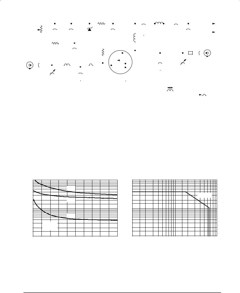
Figure 1. MRF166C 400 MHz Test Circuit
|
|
|
|
|
TYPICAL CHARACTERISTICS |
|
|
|||
|
100 |
|
|
|
|
|
|
10 |
|
|
(pF) |
50 |
|
Coss |
|
|
|
(AMPS) |
|
|
|
|
|
Ciss |
|
|
|
|
TC = 25°C |
|
||
|
|
|
|
|
|
|
|
|
||
CAPACITANCEC, |
20 |
|
|
|
|
CURRENTDRAIN |
|
|
|
|
10 |
|
|
|
|
|
1 |
|
|
||
|
|
|
|
|
|
|
|
|
||
|
5 |
|
Crss |
|
|
|
|
|
|
|
|
|
|
|
|
|
|
, |
|
|
|
|
|
VGS = 0 V |
|
|
|
|
D |
|
|
|
|
|
|
|
|
|
I |
|
|
|
|
|
2 |
f = 1 MHz |
|
|
|
|
|
|
|
|
|
1 |
5 |
10 |
15 |
20 |
25 |
|
0.1 |
10 |
100 |
|
0 |
|
0 |
|||||||
|
|
VDS, DRAIN±SOURCE VOLTAGE (VOLTS) |
|
|
|
VDS, DRAIN±SOURCE VOLTAGE (VOLTS) |
|
|||
Figure 2. Capacitance versus Drain±Source Voltage |
Figure 3. DC Safe Operating Area |
MOTOROLA RF DEVICE DATA |
MRF166C |
|
3 |
TYPICAL CHARACTERISTICS
|
35 |
|
|
|
|
|
|
|
|
|
16 |
|
|
|
|
|
|
|
|
|
, OUTPUT POWER (WATTS) |
30 |
|
|
|
|
|
|
|
|
OUTPUTPOWER (WATTS) |
14 |
|
|
|
|
|
|
|
|
|
25 |
|
|
|
|
|
|
f = 400 MHz |
|
12 |
|
|
|
|
|
|
|
|
|
||
20 |
|
|
|
|
|
|
|
|
10 |
|
|
|
|
|
|
|
f = 400 MHz |
|||
|
|
|
|
|
|
500 MHz |
|
|
|
|
|
|
|
|
|
|||||
|
|
|
|
|
|
|
|
8 |
|
|
|
|
|
|
|
|
|
|||
15 |
|
|
|
|
|
|
|
|
|
|
|
|
|
|
|
|
|
|||
|
|
|
|
|
|
|
|
6 |
|
|
|
|
|
|
|
|
|
|||
|
|
|
|
|
|
|
|
|
|
|
|
|
|
|
|
|
|
|||
10 |
|
|
|
|
|
VDS = 28 V |
|
4 |
|
|
|
|
|
|
|
|
|
|||
o |
|
|
|
|
|
|
I |
= 100 mA |
|
, |
|
|
|
|
|
|
V |
= 13.5 V |
|
|
|
|
|
|
|
|
|
o |
|
|
|
|
|
|
|
||||||
P |
|
|
|
|
|
|
DQ |
|
|
P |
|
|
|
|
|
|
|
DS |
|
|
|
5 |
|
|
|
|
|
|
|
|
|
2 |
|
|
|
|
|
|
IDQ = 100 mA |
|
|
|
0 |
0.1 |
0.2 |
0.3 |
0.4 |
0.5 |
0.6 |
0.7 |
0.8 |
|
0 |
0 |
0.1 |
0.2 |
0.3 |
0.4 |
0.5 |
0.6 |
0.7 |
0.8 |
|
0 |
|
||||||||||||||||||
Pin, INPUT POWER (WATTS) |
Pin, INPUT POWER (WATTS) |
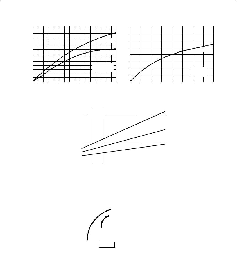
Figure 4. Output Power versus Input Power |
Figure 5. Output Power versus Input Power |
Po, OUTPUT POWER (WATTS)
32 |
|
|
|
|
|
|
|
|
|
|
|
|
|
|
|
|
|
|
f = |
400 MHz |
|
|
|
|
|
|
|
Pin = |
0.8 W |
|
|
|
|
||
|
|
|
|
|
|
|
|
|
|
|
|
|
|||||
28 |
|
I |
|
= 100 mA |
|
|
|
|
|
|
|
|
|
|
|||
|
|
DQ |
|
|
|
|
|
|
|
|
|
|
|
|
|
|
|
24 |
|
|
|
|
|
|
|
|
|
|
|
|
|
|
|
|
|
|
|
|
|
|
|
|
|
|
|
|
|
|
|
|
|
|
|
20 |
|
|
|
|
|
|
|
|
|
|
|
|
|
|
|
|
|
|
|
|
|
|
|
|
|
|
|
|
|
0.4 W |
|
|
|
|
|
16 |
|
|
|
|
|
|
|
|
|
|
|
|
|
|
|
|
|
|
|
|
|
|
|
|
|
|
|
|
|
|
|
|
|
|
|
12 |
|
|
|
|
|
|
|
|
|
|
|
|
0.2 W |
|
|
|
|
8 |
|
|
|
|
|
|
|
|
|
|
|
|
|
|
|
|
|
|
|
|
|
|
|
|
|
|
|
|
|
|
|
|
|
|
|
4 |
|
|
|
|
|
|
|
|
|
|
|
|
|
|
|
|
|
|
|
|
|
|
|
|
|
|
|
|
|
|
|
|
|
|
|
0 |
|
|
|
|
|
|
|
|
|
|
|
|
|
|
|
|
|
|
14 |
16 |
18 |
20 |
22 |
24 |
26 |
28 |
|||||||||
12 |
|||||||||||||||||
VDS, DRAIN±SOURCE (VOLTS)
Figure 6. Output Power versus Voltage
|
400 |
f = 500 MHz |
|
|
|
|
f = 500 MHz |
200 |
|
|
400 |
Zin |
|
200 |
|
|
100 |
|
ZOL* |
|
|
|
|
100 |
Zo |
= 50 Ω |
|
|
|||
VDD = 28 V, IDQ = 100 mA
f |
Zin |
|
ZOL* |
MHz |
OHMS |
|
OHMS |
|
|
|
|
|
(Pout = 20 W) |
|
|
100 |
11.0 ± j21.0 |
|
8.50 ± j10.0 |
200 |
4.20 ± j12.6 |
|
6.00 ± j9.00 |
400 |
1.90 ± j5.80 |
|
4.50 ± j6.70 |
500 |
1.50 ± j4.10 |
|
4.20 ± j5.40 |
|
|
|
|
ZOL* = Conjugate of the optimum load impedance into which the device output operates at a given output power, voltage and frequency.
|
Figure 7. Series Equivalent Input and Output Impedance |
|
|
MRF166C |
MOTOROLA RF DEVICE DATA |
4 |
|
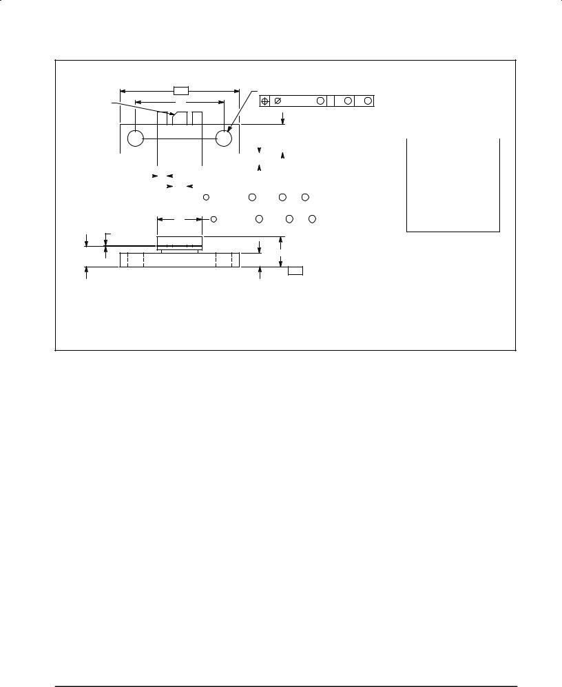
PACKAGE DIMENSIONS
|
-A- |
Q 2 PL |
|
|
|
|
|
|
IDENTIFICATION |
L |
0.15 (0.006) M |
T |
A |
M |
N |
M |
|
NOTCH |
|
|
|
|
|
|
NOTES: |
|
|
|
|
|
|
|
|
||
6 |
5 |
4 |
|
|
|
|
1. |
DIMENSIONING AND TOLERANCING PER |
|
|
|
|
|
ANSI Y14.5M, 1982. |
|||
|
|
|
|
|
|
|
|
|
|
|
|
|
|
|
|
2. |
CONTROLLING DIMENSION: INCH. |
|
|
|
|
|
|
|
|
|
|
|
|
|
|
|
|
|
|
|
|
|
|
|
|
|
|
|
|
|
|
-N- |
|
|
|
|
|
|
|
|
|
|
||
|
|
|
|
|
|
|
|
|
|
|
|
|
|
|
|
|
|
|
|
|
|
|
|
|
|
|
|
|
|
|
|
|
|
|
|
|
|
|
INCHES |
MILLIMETER |
||
|
|
|
|
|
|
|
|
|
|
|
|
|
|
|
|
|
|
|
|
|
|
|
|
|
|
|
|
|
|
|
|
|
|
|
|
|
|
DIM |
MIN |
MAX |
MIN |
MAX |
|
1 |
|
2 |
|
3 |
|
|
|
|
|
|
|
|
|
|
|
|
K |
|
|
|
|
|
|
|
|
|
|
A |
0.965 |
0.985 |
24.52 |
25.01 |
|||||||||
|
|
|
|
|
|
|
|
|
|
|
|
|
|
|
|
|
|
|
|
|
|
|
|
|
|
|
|
|
|
|
|
|
|
|
B |
0.355 |
0.375 |
9.02 |
9.52 |
|||
|
|
|
|
|
|
|
|
|
|
|
|
|
|
|
|
|
|
|
|
|
|
|
|
|
|
|
|
|
|
|
|
|
|
|
|
|
|
C |
0.230 |
0.260 |
5.85 |
6.60 |
|
|
F |
|
|
|
|
|
|
|
|
|
|
|
|
|
|
|
|
|
|
|
|
|
|
|
|
|
|
|
|
|
|
|
|
|
D |
0.115 |
0.125 |
2.93 |
3.17 |
||
|
|
|
|
|
|
|
|
|
|
|
|
|
|
|
|
|
|
|
|
|
|
|
|
|
|
|
|
|
|
|
|
|
|
|||||||||
|
|
|
|
|
|
|
|
|
|
|
|
|
|
D 2 PL |
|
|
|
|
|
|
|
|
|
|
E |
0.102 |
0.114 |
2.59 |
2.90 |
|||||||||||||
|
|
|
|
|
|
|
|
|
|
|
|
|
|
|
|
|
|
|
|
|
|
|
|
F |
0.075 |
0.085 |
1.91 |
2.15 |
||||||||||||||
|
|
|
|
|
|
|
|
|
|
|
|
|
|
|
|
|
|
|
|
|
|
|
|
|||||||||||||||||||
|
|
|
|
|
|
|
|
|
|
|
|
|
|
|
|
|
|
|
0.38 (0.015) M |
T |
A |
M |
|
N M |
|
|
H |
0.160 |
0.170 |
4.07 |
4.31 |
|||||||||||
|
|
|
|
|
|
|
|
|
|
|
|
|
|
|
|
|
|
|
|
|
||||||||||||||||||||||
|
|
|
|
|
|
|
|
|
|
|
|
|
|
|
|
|
J |
0.004 |
0.006 |
0.11 |
0.15 |
|||||||||||||||||||||
|
|
|
|
|
|
|
|
|
|
|
|
|
|
|
|
|
|
|
|
|
|
|
|
|
|
|
|
|
|
|
|
|
|
|
|
|
|
|||||
|
|
|
|
|
|
|
|
|
|
|
|
|
|
|
|
|
|
|
|
|
|
|
|
|
|
|
|
|
|
|
|
|
|
|
|
|
|
K |
0.090 |
0.110 |
2.29 |
2.79 |
|
|
|
|
|
|
|
|
|
B |
|
|
|
|
|
|
|
|
|
|
|
|
|
|
|
|
|
|
|
|
|
|
|
|
|
|
|
L |
0.725 BSC |
18.42 BSC |
|||
|
|
|
|
|
|
|
|
|
|
|
|
|
|
|
|
|
|
|
0.38 (0.015) M |
T |
|
A M |
|
N M |
|
|||||||||||||||||
|
|
|
|
|
|
|
|
|
|
|
|
|
|
|
|
|
|
|
|
|
|
N |
0.225 |
0.241 |
5.72 |
6.12 |
||||||||||||||||
|
|
|
|
|
|
|
|
|
|
|
|
|
|
|
|
|
|
|
|
|
|
|
|
|
|
|
|
|
|
|
|
|
|
|
|
|
|
Q |
0.125 |
0.135 |
3.18 |
3.42 |
|
J |
|
|
|
|
|
|
STYLE 3: |
|
|
C |
|
PIN 1. |
SOURCE (COMMON) |
H |
|
2. |
GATE (INPUT) |
|
E |
|
|||
|
|
3. |
SOURCE (COMMON) |
|
|
-T- |
SEATING |
4. |
SOURCE (COMMON) |
|
5. |
DRAIN (OUTPUT) |
||
|
|
PLANE |
||
|
|
|
6. |
SOURCE (COMMON) |
CASE 319±07
ISSUE M
MOTOROLA RF DEVICE DATA |
MRF166C |
|
5 |

Motorola reserves the right to make changes without further notice to any products herein. Motorola makes no warranty, representation or guarantee regarding the suitability of its products for any particular purpose, nor does Motorola assume any liability arising out of the application or use of any product or circuit, and specifically disclaims any and all liability, including without limitation consequential or incidental damages. ªTypicalº parameters can and do vary in different applications. All operating parameters, including ªTypicalsº must be validated for each customer application by customer's technical experts. Motorola does not convey any license under its patent rights nor the rights of others. Motorola products are not designed, intended, or authorized for use as components in systems intended for surgical implant into the body, or other applications intended to support or sustain life, or for any other application in which the failure of the Motorola product could create a situation where personal injury or death may occur. Should Buyer purchase or use Motorola products for any such unintended or unauthorized application, Buyer shall indemnify and hold Motorola and its officers, employees, subsidiaries, affiliates, and distributors harmless against all claims, costs, damages, and expenses, and reasonable attorney fees arising out of, directly or indirectly, any claim of personal injury or death associated with such unintended or unauthorized use, even if such claim alleges that Motorola was negligent regarding the design or manufacture of the part. Motorola and  are registered trademarks of Motorola, Inc. Motorola, Inc. is an Equal Opportunity/Affirmative Action Employer.
How to reach us: |
|
USA / EUROPE: Motorola Literature Distribution; |
JAPAN: Nippon Motorola Ltd.; Tatsumi±SPD±JLDC, Toshikatsu Otsuki, |
P.O. Box 20912; Phoenix, Arizona 85036. 1±800±441±2447 |
6F Seibu±Butsuryu±Center, 3±14±2 Tatsumi Koto±Ku, Tokyo 135, Japan. 03±3521±8315 |
MFAX: RMFAX0@email.sps.mot.com ± TOUCHTONE (602) 244±6609 HONG KONG: Motorola Semiconductors H.K. Ltd.; 8B Tai Ping Industrial Park, |
|
INTERNET: http://Design±NET.com |
51 Ting Kok Road, Tai Po, N.T., Hong Kong. 852±26629298 |
◊ |
MRF166C/D |
|
*MRF166C/D* |