

MOTOROLA
SEMICONDUCTOR TECHNICAL DATA
Order this document by MRF9745T1/D
Advance |
Information |
|
|
The RF Small Signal Line |
|
MRF9745T1 |
|
Silicon |
Lateral |
FET |
|
|
|||
N±Channel Enhancement±Mode MOSFET
Designed for use in low voltage, moderate power amplifiers such as portable analog and digital cellular radios and PC RF modems.
•Performance Specifications at 5.8 V, 900 MHz: Output Power = 30 dBm Min
Power Gain = 10 dB Typ Efficiency = 50% Min
•Guaranteed Ruggedness at Load VSWR = 20:1
•New Plastic Surface Mount Package
•Available in Tape and Reel Packaging.
T1 Suffix = 1,000 Units per 8 mm, 7 inch Reel
•Device Marking = 9745
MAXIMUM RATINGS
30 dBm, 900 MHz HIGH FREQUENCY POWER TRANSISTOR LDMOS FET
CASE 449±02, STYLE 1 (PLD±1)
Rating |
|
Symbol |
|
Value |
Unit |
|
|
|
|
|
|
|
|
Drain±Source Voltage |
|
VDSS |
|
35 |
Vdc |
|
Drain±Gate Voltage (RGS = 1 MΩ) |
|
VDGO |
|
25 |
Vdc |
|
Gate±Source Voltage |
|
VGS |
|
± 10 |
Vdc |
|
Drain Current ± Continuous |
|
ID |
|
2 |
Adc |
|
Total Device Dissipation @ TC = 50°C |
|
PD |
|
10 |
W |
|
Derate above 50°C |
|
|
|
100 |
mW/°C |
|
|
|
|
|
|
|
|
Storage Temperature Range |
|
Tstg |
± 65 to +150 |
°C |
||
Operating Temperature Range |
|
TJ |
|
150 |
°C |
|
THERMAL CHARACTERISTICS |
|
|
|
|
|
|
|
|
|
|
|
|
|
Characteristic |
|
Symbol |
|
Max |
Unit |
|
|
|
|
|
|
|
|
Thermal Resistance, Junction to Case |
|
RθJC |
|
10 |
°C/W |
|
ELECTRICAL CHARACTERISTICS (TC = 25°C unless otherwise noted) |
|
|
|
|
|
|
Characteristic |
Symbol |
Min |
Typ |
|
Max |
Unit |
|
|
|
|
|
|
|
OFF CHARACTERISTICS |
|
|
|
|
|
|
|
|
|
|
|
|
|
Drain±Source Leakage Current |
IDSS |
± |
± |
|
10 |
μAdc |
(VDS = 35 V, VGS = 0) |
|
|
|
|
|
|
Gate±Source Leakage Current |
IGSS |
± |
± |
|
1 |
μAdc |
(VGS = 5 V, VDS = 0) |
|
|
|
|
|
|
NOTE ± CAUTION ± MOS devices are susceptible to damage from electrostatic charge. Reasonable precautions in handling and packaging MOS devices should be observed.
REV 1
MOTOROLAMotorola, Inc. 1997RF DEVICE DATA |
MRF9745T1 |
|
1 |

ELECTRICAL CHARACTERISTICS ± continued (TC = 25°C unless otherwise noted)
Characteristic |
Symbol |
Min |
Typ |
Max |
Unit |
|
|
|
|
|
|
ON CHARACTERISTICS |
|
|
|
|
|
|
|
|
|
|
|
Gate Threshold Voltage |
VGS(th) |
1 |
2 |
3 |
Vdc |
(VDS = 6 V, ID = 25 μA) |
|
|
|
|
|
Forward Transconductance |
gfs |
± |
550 |
± |
mmhos |
(VDS = 6 V, ID = 200 mA) |
|
|
|
|
|
Resistance Drain±Source |
RDS(on) |
± |
1 |
2.5 |
Ω |
(VGS = 4 V, ID = 100 mA) |
|
|
|
|
|
DYNAMIC CHARACTERISTICS |
|
|
|
|
|
|
|
|
|
|
|
Input Capacitance |
Ciss |
± |
14 |
± |
pF |
(VDS = 6 V, VGS = 0, f = 1 MHz) |
|
|
|
|
|
Output Capacitance |
Coss |
± |
11 |
± |
pF |
(VDS = 6 V, VGS = 0, f = 1 MHz) |
|
|
|
|
|
Feedback Capacitance |
Crss |
± |
1.8 |
± |
pF |
(VDS = 6 V, VGS = 0, f = 1 MHz) |
|
|
|
|
|
FUNCTIONAL CHARACTERISTICS |
|
|
|
|
|
|
|
|
|
|
|
Power Gain |
Gps |
9.5 |
10 |
± |
dB |
(VDD = 5.8 Vdc, Pin = 20 dBm, IDQ = 150 mA, f = 900 MHz) |
|
|
|
|
|
Drain Efficiency |
ηD |
50 |
55 |
± |
% |
(VDD = 5.8 Vdc, Pin = 20 dBm, IDQ = 150 mA, f = 900 MHz) |
|
|
|
|
|
Ruggedness Test |
Ψ |
|
|
|
|
(VDD = 5.8 Vdc, Pin = 20 dBm, IDQ = 150 mA, f = 900 MHz, |
|
No Degradation in Output Power after Test |
|||
Load VSWR = 20:1, All Phase Angles at Frequency Test) |
|
|
|
|
|
|
|
|
|
|
|
Table 1. Large Signal Impedance
VDD = 5.8 V, Pin = 20 dBm, IDQ = 150 mA
f |
Zin |
ZOL* |
MHz |
Ohms |
Ohms |
|
|
|
850 |
7.0 ± j6.4 |
6.1 ± j5.1 |
|
|
|
900 |
5.2 ± j6.5 |
5.9 ± j4.6 |
|
|
|
950 |
5.2 ± j6.0 |
6.1 ± j4.7 |
|
|
|
ZOL* is the conjugate of the optimum load impedance into which the device output operates at a given output power, voltage and frequency.
MRF9745T1 |
MOTOROLA RF DEVICE DATA |
2 |
|
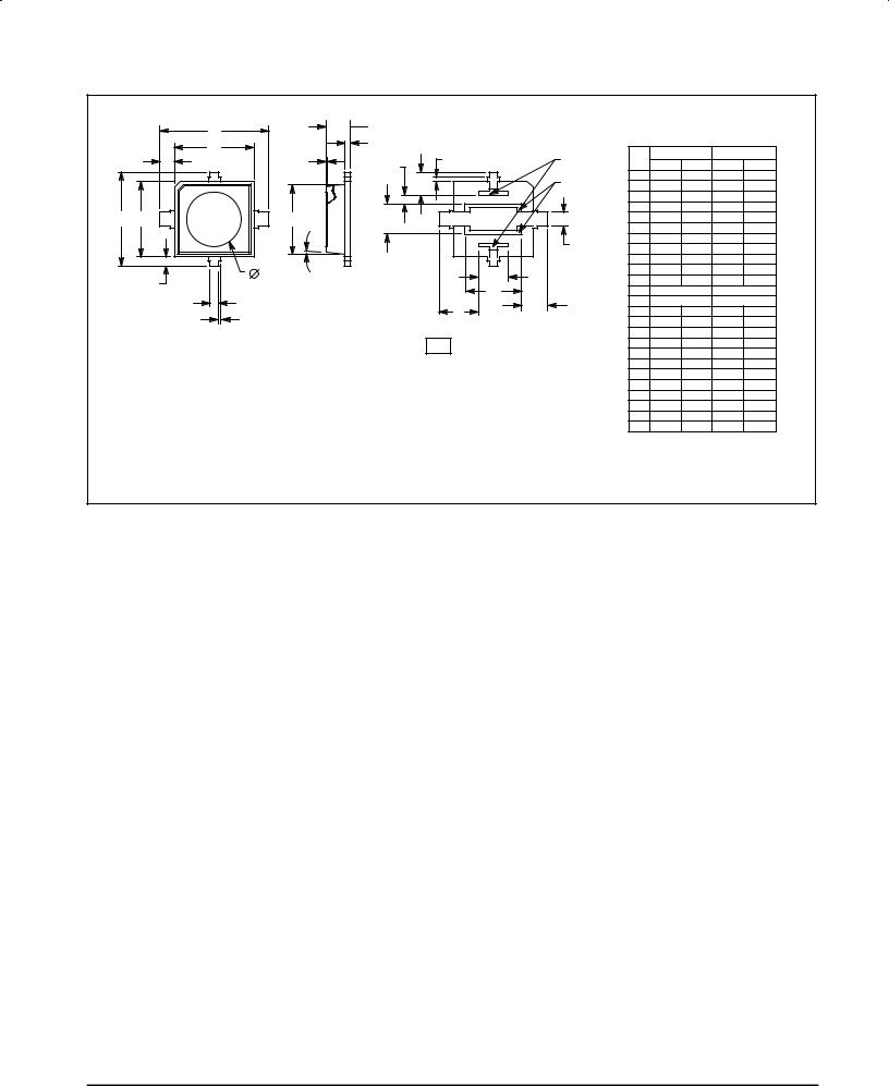
PACKAGE DIMENSIONS
|
|
|
L |
|
|
S |
A |
|
|
|
|
|
|
|
1 |
R |
B |
4 |
3 |
|
|
|
2 |
|
|
K |
Q |
|
|
|
|
|
|
D 2 PL |
|
|
|
|
J 8 PL |
NOTES:
1. DIMENSIONING AND TOLERANCING PER ANSI C  Y14.5M, 1982.
2. CONTROLLING DIMENSION: INCH.
|
E |
|
|
|
|
INCHES |
MILLIMETERS |
||
P |
W 8 PL |
|
ZONE U |
|
|||||
|
DIM |
MIN |
MAX |
MIN |
MAX |
||||
|
H |
|
|
|
|||||
|
T |
|
ZONE V |
A |
0.185 |
0.195 |
4.70 |
4.95 |
|
|
|
B |
0.175 |
0.185 |
4.44 |
4.70 |
|||
|
|
|
|
|
|||||
|
|
|
|
|
C |
0.058 |
0.064 |
1.47 |
1.63 |
|
G |
|
|
|
D |
0.017 |
0.023 |
0.43 |
0.58 |
N |
|
|
|
E |
0.014 |
0.017 |
0.36 |
0.43 |
|
|
|
|
|
|
F |
0.027 |
0.033 |
0.69 |
0.84 |
|
|
|
F |
2 PL |
G |
0.071 |
0.077 |
1.80 |
1.96 |
|
|
|
H |
0.017 |
0.023 |
0.43 |
0.58 |
||
|
|
|
|
|
|||||
|
|
|
|
|
J |
0.000 |
0.007 |
0.00 |
0.18 |
M |
Y |
|
|
|
K |
0.018 |
0.026 |
0.46 |
0.66 |
|
|
|
L |
0.253 |
0.263 |
6.43 |
6.68 |
||
DRAFT |
X |
|
|
|
M |
5 |
REF |
5 |
REF |
4 PL |
|
|
|
||||||
|
Z |
AA |
|
|
N |
1.75 REF |
4.44 REF |
||
|
|
|
P |
0.000 |
0.006 |
0.00 |
0.15 |
||
|
|
|
|
||||||
|
|
|
|
|
Q |
0.120 |
0.130 |
3.05 |
3.30 |
|
RESIN BLEED/FLASH |
|
|
R |
0.220 |
0.230 |
5.59 |
5.84 |
|
|
|
|
S |
0.030 |
0.038 |
0.76 |
0.97 |
||
|
ALLOWABLE |
|
|
|
T |
0.050 |
0.060 |
1.27 |
1.52 |
|
|
|
|
|
U |
0.000 |
0.018 |
0.00 |
0.46 |
|
|
|
|
|
V |
0.000 |
0.014 |
0.00 |
0.36 |
|
|
|
|
|
W |
0.004 |
0.016 |
0.10 |
0.41 |
|
|
|
|
|
X |
0.131 |
0.141 |
3.33 |
3.58 |
|
|
|
|
|
Y |
0.065 |
0.075 |
1.65 |
1.90 |
|
|
|
|
|
Z |
0.089 |
0.099 |
2.26 |
2.51 |
|
|
|
|
|
AA |
0.056 |
0.066 |
1.42 |
1.67 |
CASE 449±02 ISSUE
STYLE 1:
PIN 1. DRAIN
2.GATE
3.SOURCE
4.SOURCE
MOTOROLA RF DEVICE DATA |
MRF9745T1 |
|
3 |

Motorola reserves the right to make changes without further notice to any products herein. Motorola makes no warranty, representation or guarantee regarding the suitability of its products for any particular purpose, nor does Motorola assume any liability arising out of the application or use of any product or circuit, and specifically disclaims any and all liability, including without limitation consequential or incidental damages. ªTypicalº parameters which may be provided in Motorola data sheets and/or specifications can and do vary in different applications and actual performance may vary over time. All operating parameters, including ªTypicalsº must be validated for each customer application by customer's technical experts. Motorola does not convey any license under its patent rights nor the rights of others. Motorola products are not designed, intended, or authorized for use as components in systems intended for surgical implant into the body, or other applications intended to support or sustain life, or for any other application in which the failure of the Motorola product could create a situation where personal injury or death may occur. Should Buyer purchase or use Motorola products for any such unintended or unauthorized application, Buyer shall indemnify and hold Motorola and its officers, employees, subsidiaries, affiliates, and distributors harmless against all claims, costs, damages, and expenses, and reasonable attorney fees arising out of, directly or indirectly, any claim of personal injury or death associated with such unintended or unauthorized use, even if such claim alleges that Motorola was negligent regarding the design or manufacture of the part. Motorola and  are registered trademarks of Motorola, Inc. Motorola, Inc. is an Equal Opportunity/Affirmative Action Employer.
|
Mfax is a trademark of Motorola, Inc. |
How to reach us: |
|
USA / EUROPE / Locations Not Listed: Motorola Literature Distribution; |
JAPAN: Nippon Motorola Ltd.; Tatsumi±SPD±JLDC, 6F Seibu±Butsuryu±Center, |
P.O. Box 5405, Denver, Colorado 80217. 303±675±2140 or 1±800±441±2447 |
3±14±2 Tatsumi Koto±Ku, Tokyo 135, Japan. 81±3±3521±8315 |
Mfax : RMFAX0@email.sps.mot.com ± TOUCHTONE 602±244±6609 |
ASIA/PACIFIC: Motorola Semiconductors H.K. Ltd.; 8B Tai Ping Industrial Park, |
INTERNET: http://www.mot.com/sps/ |
51 Ting Kok Road, Tai Po, N.T., Hong Kong. 852±26629298 |
MRF9745T1 |
◊ |
MOTOROLA RF DEVICEMRF9745DATA1/D |
4 |
|
|