

MOTOROLA
SEMICONDUCTOR TECHNICAL DATA
Order this document by MRF16030/D
The RF Line
NPN Silicon
RF Power Transistor
Designed for 28 Volt microwave large±signal, common base, Class±C CW amplifier applications in the range 1600 ± 1640 MHz.
•Specified 28 Volt, 1.6 GHz Class±C Characteristics Output Power = 30 Watts
Minimum Gain = 7.5 dB, @ 30 Watts Minimum Efficiency = 40% @ 30 Watts
•Characterized with Series Equivalent Large±Signal Parameters from 1500 MHz to 1700 MHz
•Silicon Nitride Passivated
•Gold Metallized, Emitter Ballasted for Long Life and Resistance to Metal Migration
•Circuit board photomaster available upon request by contacting RF Tactical Marketing in Phoenix, AZ.
MAXIMUM RATINGS (TJ = 25°C unless otherwise noted)
MRF16030
30 WATTS, 1.6 GHz
RF POWER TRANSISTOR
NPN SILICON
CASE 395C±01, STYLE 2
Rating |
Symbol |
Value |
Unit |
|
|
|
|
Collector±Emitter Voltage |
VCES |
60 |
Vdc |
Emitter±Base Voltage |
VEBO |
4.0 |
Vdc |
Collector±Current |
IC |
4.0 |
Adc |
Total Device Dissipation @ TC = 25°C |
PD |
103 |
Watts |
Derate above 25°C |
|
0.58 |
°C/W |
|
|
|
|
Storage Temperature Range |
Tstg |
± 65 to +150 |
°C |
THERMAL CHARACTERISTICS |
|
|
|
|
|
|
|
Thermal Resistance Ð Junction to Case (1) (2) |
RθJC |
1.7 |
°C/W |
(1)Thermal measurement performed using CW RF operating condition.
(2)Thermal resistance is determined under specified RF operating conditions by infrared measurement techniques.
REV 3
MOTOROLAMotorola, Inc. 1997RF DEVICE DATA |
MRF16030 |
|
1 |

ELECTRICAL CHARACTERISTICS (TC = 25°C unless otherwise noted)
Characteristic |
Symbol |
Min |
Typ |
Max |
Unit |
|
|
|
|
|
|
OFF CHARACTERISTICS
Collector±Emitter Breakdown Voltage |
V(BR)CES |
|
|
|
|
Vdc |
(IC = 100 mAdc, VBE = 0) |
|
55 |
|
Ð |
Ð |
|
Collector±Base Breakdown Voltage |
V(BR)CBO |
|
|
|
|
Vdc |
(IC = 100 mAdc, IE = 0) |
|
55 |
|
Ð |
Ð |
|
Emitter±Base Breakdown Voltage |
V(BR)EBO |
4.0 |
|
|
|
Vdc |
(IE = 10 mAdc, IC = 0) |
|
|
|
Ð |
Ð |
|
Collector Cutoff Current |
ICES |
|
|
|
|
mAdc |
(VCE = 28 Vdc, VBE = 0) |
|
Ð |
|
Ð |
10 |
|
ON CHARACTERISTICS |
|
|
|
|
|
|
|
|
|
|
|
|
|
DC Current Gain |
hFE |
|
|
|
|
Ð |
(ICE = 1.0 Adc, VCE = 5.0 Vdc) |
|
20 |
|
35 |
80 |
|
FUNCTIONAL TESTS |
|
|
|
|
|
|
|
|
|
|
|
|
|
Collector±Base Amplifier Power Gain |
Gpe |
|
|
|
|
dB |
(VCC = 28 Vdc, Pout = 30 Watts, f = 1600/1640 MHz) |
|
7.5 |
|
7.7 |
Ð |
|
Collector Efficiency |
η |
|
|
|
|
% |
(VCC = 28 Vdc, Pout = 30 Watts, f = 1600/1640 MHz) |
|
40 |
|
45 |
Ð |
|
Input Return Loss |
IRL |
|
|
|
|
dB |
(VCC = 28 Vdc, Pout = 30 Watts, f = 1600/1640 MHz) |
|
8.0 |
|
Ð |
Ð |
|
Output Mismatch Stress |
Ψ |
|
|
|
|
|
VCC = 28 Vdc, Pout = 30 Watts, f = 1600 MHz, Load |
|
|
No Degradation in Output Power |
|||
VSWR = 3:1, All phase angles at frequency of test |
|
|
|
|
|
|
|
|
|
|
|
|
|
MRF16030 |
MOTOROLA RF DEVICE DATA |
2 |
|
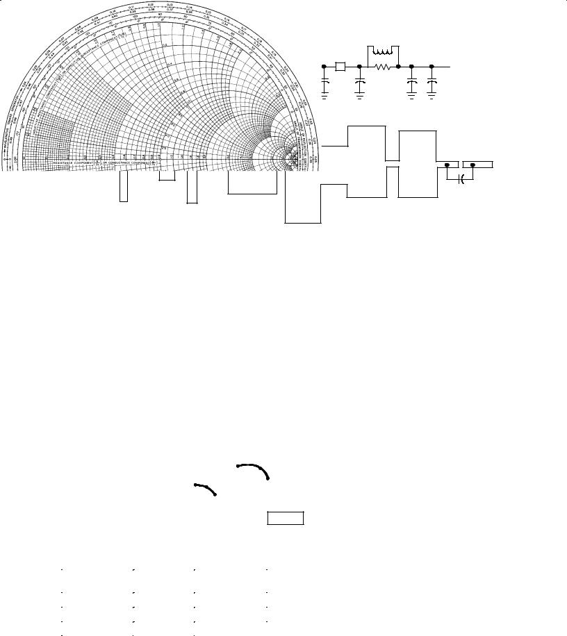
L3
B1
 28 Vdc
R1
C1 |
C2 |
C3 |
C4 |
L2 

L1 


C5
|
Board Material ± Teflon |
Glass Laminate Dielectric |
||
|
Thickness = 0.30″ , er = 2.55″ , 2.0 oz. Copper |
|
|
|
B1 |
Fair Rite Bead on #24 Wire |
C4 |
47 mF, 50 V, Electrolytic |
|
C1, C5 100 pF, B Case, ATC Chip Cap |
L1, L2 |
3 |
Turns, #18, 0.133″ ID, 0.15″ Long |
|
C2 |
0.1 mF, Dipped Mica Cap |
L3 |
9 |
Turns, #24 Enamel |
C3 |
0.1 mF, Chip Cap |
R1 |
82 W, 1.0 W, Carbon |
|
Figure 1. MRF16030 Test Fixture Schematic
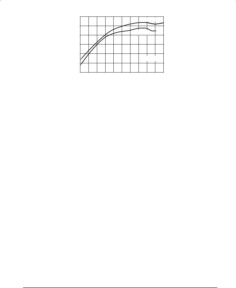
|
f = 1.5 GHz |
1.6 GHz |
|
|
|
1.7 GHz |
1.6 GHz |
Zin |
|
1.7 GHz |
|
|
|
|
ZOL* |
f = 1.5 GHz |
|
Zo = 10 W
VCC = 28 Vdc, Pout = 30 W
f |
Zin |
ZOL* |
MHz |
Ohms |
Ohms |
|
|
|
1500 |
3.05 + j 4.88 |
2.66 + j 2.53 |
|
|
|
1600 |
4.32 + j 6.00 |
1.79 + j 2.80 |
|
|
|
1700 |
5.62 + j 5.79 |
1.51 + j 2.64 |
|
|
|
ZOL* = Conjugate of the optimum load impedance into which the device output operates at a given output power, voltage and frequency.
|
Figure 2. Series Equivalent Input/Output Impedance |
|
|
MOTOROLA RF DEVICE DATA |
MRF16030 |
|
3 |
|
45 |
|
|
|
|
|
|
|
f = 1.6 GHz |
|
|
(WATTS) |
|
|
|
|
|
|
|
|
|
||
40 |
|
|
|
|
|
|
|
|
|
|
|
|
|
|
|
|
|
|
|
|
|
|
|
|
35 |
|
|
|
|
|
|
1.64 GHz |
|
|
|
POWER |
|
|
|
|
|
|
|
|
|
|
|
30 |
|
|
|
|
|
|
|
|
|
|
|
OUTPUT, |
|
|
|
|
|
|
|
|
|
|
|
25 |
|
|
|
|
|
|
|
|
|
|
|
|
|
|
|
|
|
|
|
|
|
|
|
out |
|
|
|
|
|
|
|
|
VCC = 28 Vdc |
|
|
P |
20 |
|
|
|
|
|
|
|
|
|
|
|
|
|
|
|
|
|
|
|
|
|
|
|
15 |
4.5 |
5.0 |
5.5 |
6.0 |
6.5 |
7.0 |
7.5 |
8.0 |
8.5 |
9.0 |
|
4.0 |
||||||||||
|
|
|
|
Pin, INPUT POWER (WATTS) |
|
|
|
||||
Figure 3. Output Power versus Input Power
MRF16030 |
MOTOROLA RF DEVICE DATA |
4 |
|
PACKAGE DIMENSIONS
|
±A± |
|
|
U |
Q 2 PL |
|
|
|
1 |
|
0.51 (0.020) M T A M B M |
|
±B± |
|
3 |
K |
|
2 |
|
D |
|
N |
E |
J |
|
H |
C |
|
±T± SEATING PLANE
CASE 395C±01
ISSUE A
NOTES:
1.DIMENSIONING AND TOLERANCING PER ANSI Y14.5M, 1982.
2.CONTROLLING DIMENSION: INCH.
|
INCHES |
MILLIMETERS |
||
DIM |
MIN |
MAX |
MIN |
MAX |
A |
0.739 |
0.750 |
18.77 |
19.05 |
B |
0.240 |
0.260 |
6.10 |
6.60 |
C |
0.165 |
0.198 |
4.19 |
5.03 |
D |
0.215 |
0.225 |
5.46 |
5.72 |
E |
0.055 |
0.070 |
1.40 |
1.78 |
H |
0.079 |
0.091 |
2.01 |
2.31 |
J |
0.004 |
0.006 |
0.10 |
0.15 |
K |
0.210 |
0.240 |
5.33 |
6.10 |
N |
0.315 |
0.330 |
8.00 |
8.38 |
Q |
0.125 |
0.135 |
3.18 |
3.42 |
U |
0.560 BSC |
14.23 BSC |
||
STYLE 2:
PIN 1. EMITTER
2.COLLECTOR
3.BASE
MOTOROLA RF DEVICE DATA |
MRF16030 |
|
5 |

Motorola reserves the right to make changes without further notice to any products herein. Motorola makes no warranty, representation or guarantee regarding the suitability of its products for any particular purpose, nor does Motorola assume any liability arising out of the application or use of any product or circuit, and specifically disclaims any and all liability, including without limitation consequential or incidental damages. ªTypicalº parameters which may be provided in Motorola data sheets and/or specifications can and do vary in different applications and actual performance may vary over time. All operating parameters, including ªTypicalsº must be validated for each customer application by customer's technical experts. Motorola does not convey any license under its patent rights nor the rights of others. Motorola products are not designed, intended, or authorized for use as components in systems intended for surgical implant into the body, or other applications intended to support or sustain life, or for any other application in which the failure of the Motorola product could create a situation where personal injury or death may occur. Should Buyer purchase or use Motorola products for any such unintended or unauthorized application, Buyer shall indemnify and hold Motorola and its officers, employees, subsidiaries, affiliates, and distributors harmless against all claims, costs, damages, and expenses, and reasonable attorney fees arising out of, directly or indirectly, any claim of personal injury or death associated with such unintended or unauthorized use, even if such claim alleges that Motorola was negligent regarding the design or manufacture of the part. Motorola and  are registered trademarks of Motorola, Inc. Motorola, Inc. is an Equal Opportunity/Affirmative Action Employer.
|
Mfax is a trademark of Motorola, Inc. |
How to reach us: |
|
USA / EUROPE / Locations Not Listed: Motorola Literature Distribution; |
JAPAN: Nippon Motorola Ltd.: SPD, Strategic Planning Office, 4±32±1, |
P.O. Box 5405, Denver, Colorado 80217. 303±675±2140 or 1±800±441±2447 |
Nishi±Gotanda, Shinagawa±ku, Tokyo 141, Japan. 81±3±5487±8488 |
Mfax : RMFAX0@email.sps.mot.com ± TOUCHTONE 602±244±6609 |
ASIA/PACIFIC: Motorola Semiconductors H.K. Ltd.; 8B Tai Ping Industrial Park, |
± US & Canada ONLY 1±800±774±1848 51 Ting Kok Road, Tai Po, N.T., Hong Kong. 852±26629298
INTERNET: http://motorola.com/sps
MRF16030 |
◊ |
MOTOROLA RF DEVICEMRF16030/DDATA |
6 |
|
|