

MOTOROLA
SEMICONDUCTOR TECHNICAL DATA
Order this document by MRF587/D
The RF Line
NPN Silicon
High-Frequency Transistor
. . . designed for use in high±gain, low±noise, ultra±linear, tuned and wideband amplifiers. Ideal for use in CATV, MATV, and instrumentation applications.
• Low Noise Figure Ð
NF = 3.0 dB (Typ) @ f = 500 MHz, IC = 90 mA
• High Power Gain Ð
GU(max) = 16.5 dB (Typ) @ f = 500 MHz
•Ion Implanted
•All Gold Metal System
•High fT Ð 5.5 GHz
•Low Intermodulation Distortion:
TB3 = ±70 dB DIN = 125 dB μV
•Nichrome Emitter Ballast Resistors
MAXIMUM RATINGS
Rating |
Symbol |
Value |
Unit |
|
|
|
|
Collector±Emitter Voltage |
VCEO |
17 |
Vdc |
Collector±Base Voltage |
VCBO |
34 |
Vdc |
Emitter±Base Voltage |
VEBO |
2.5 |
Vdc |
Collector Current Ð Continuous |
IC |
200 |
mAdc |
Total Device Dissipation @ TC = 50°C |
PD |
5.0 |
Watts |
Derate above TC = 50°C |
|
33 |
mW/°C |
Storage Temperature Range |
Tstg |
± 65 to +150 |
°C |
Junction Temperature |
TJ |
200 |
°C |
ELECTRICAL CHARACTERISTICS (TC = 25°C unless otherwise noted.)
MRF587
NF = 3.0 dB @ 0.5 GHz HIGH±FREQUENCY TRANSISTOR
NPN SILICON
CASE 244A±01, STYLE 1
Characteristic |
Symbol |
Min |
Typ |
Max |
Unit |
|
|
|
|
|
|
OFF CHARACTERISTICS
Collector±Emitter Breakdown Voltage |
V(BR)CEO |
17 |
Ð |
Ð |
Vdc |
(IC = 5.0 mAdc, IB = 0) |
|
|
|
|
|
Collector±Base Breakdown Voltage |
V(BR)CBO |
34 |
Ð |
Ð |
Vdc |
(IC = 1.0 mAdc, IE = 0) |
|
|
|
|
|
Emitter±Base Breakdown Voltage |
V(BR)EBO |
2.5 |
Ð |
Ð |
Vdc |
(IC = 0, IE = 0.1 mAdc) |
|
|
|
|
|
Collector Cutoff Current |
ICBO |
Ð |
Ð |
50 |
μAdc |
(VCB = 10 Vdc, IE = 0) |
|
|
|
|
|
ON CHARACTERISTICS |
|
|
|
|
|
|
|
|
|
|
|
DC Current Gain (1) |
hFE |
50 |
Ð |
200 |
Ð |
(IC = 50 mAdc, VCE = 5.0 Vdc) |
|
|
|
|
|
NOTE: |
|
|
|
|
(continued) |
1. 300 μs pulse on Tektronix 576 or equivalent. |
|
|
|
|
|
REV 6
Motorola, Inc. 1994

ELECTRICAL CHARACTERISTICS Ð continued (TC = 25°C unless otherwise noted.)
|
Characteristic |
Symbol |
Min |
Typ |
Max |
Unit |
|
|
|
|
|
|
|
|
|
|
|
|
|
|
Current±Gain Ð Bandwidth Product (2) |
fT |
Ð |
5.5 |
Ð |
GHz |
|
(IC = 90 mAdc, VCE = 15 Vdc, f = 0.5 GHz) |
|
|
|
|
|
|
Collector±Base Capacitance |
Ccb |
Ð |
1.7 |
2.2 |
pF |
|
(VCB = 10 Vdc, IE = 0, f = 1.0 MHz) |
|
|
|
|
|
|
FUNCTIONAL TESTS |
|
|
|
|
|
|
|
|
|
|
|
|
|
Narrowband Ð Figure 15 |
|
|
|
|
|
dB |
(IC = 90 mA, VCC = 15 V, f = 0.5 GHz) |
|
|
|
|
|
|
Noise Figure |
|
NF |
Ð |
3.0 |
4.0 |
|
Power Gain at Optimum Noise Figure |
GNF |
11 |
13 |
Ð |
|
|
Broadband Ð Figure 16 |
|
|
|
|
|
dB |
(IC = 90 mA, VCC = 15 V, f = 0.3 GHz) |
|
|
|
|
|
|
Noise Figure |
|
NF |
Ð |
6.3 |
Ð |
|
Power Gain at Optimum Noise Figure |
GNF |
Ð |
11 |
Ð |
|
|
Triple Beat Distortion |
|
TB3 |
Ð |
± 70 |
Ð |
dB |
(IC = 50 mA, VCC = 15 V, PRef = 50 dBmV) |
|
|
|
|
|
|
(IC = 90 mA, VCC = 15 V, PRef = 50 dBmV) |
|
|
|
|
|
|
DIN 45004 |
|
DIN |
Ð |
125 |
Ð |
dBμV |
(IC = 90 mA, VCC = 15 V) |
|
|
|
|
|
|
(IC = 90 mA, VCC = 15 V) |
|
|
|
|
|
|
Maximum Available Power Gain (3) |
GUmax |
Ð |
16.5 |
Ð |
dB |
|
(IC = 90 mA, VCE = 15 Vdc, f = 0.5 GHz) |
|
|
|
|
|
|
NOTES: |
|
|
|
|
|
|
2. Characterized on HP8542 Automatic Network Analyzer |
|
|
|
|
|
|
|S |
|2 |
|
|
|
|
|
21 |
|
|
|
|
|
|
DYNAMIC CHARACTERISTICS |
|
|
|
|
|
|
3. GUmax = (1 ±|S11|2)(1 ±|S22|2)
|
10 |
|
|
|
|
|
9 |
|
(dB) |
8 |
|
7 |
|
|
FIGURE |
6 |
|
|
|
|
NOISE |
5 |
|
4 |
|
|
|
|
|
NF, |
3 |
|
|
|
|
|
2 |
|
|
1 |
|
|
0 |
|
|
0.1 |
|
|
|
|
|
30 |
|
6 |
|
|
|
|
|
|
|
VCE = 15 V |
27 |
(dB) |
|
VCE = 15 V |
|
|
|
|
|
|
|
|
|
|
|
|||
|
|
|
IC = 90 mA |
24 |
5 |
f = 300 MHz |
|
|
|
|
GNF |
|
|
|
21 |
FIGURENOISEATGAIN |
(dB)FIGURENOISENF, |
|
|
|
|
|
|
|
|
|
|
|
|
|
||
|
|
|
|
|
|
|
|
|
|
|
|
|
|
|
18 |
|
4 |
|
|
|
|
|
|
|
|
15 |
|
|
|
|
|
|
|
|
|
|
12 |
|
3 |
|
|
|
|
N.F. |
|
|
|
9 |
|
|
|
|
|
|
|
|
|
|
, |
|
|
|
|
|
|
|
|
|
|
6 |
NF |
2 |
|
|
|
|
|
|
|
|
3 |
G |
|
|
|
|
|
|
|
|
|
|
|
|
|
|
|
|
|
|
|
|
0 |
|
1 |
|
|
|
|
0.2 |
0.3 |
0.5 |
0.7 |
0.9 10 |
|
0 |
50 |
100 |
150 |
200 |
f, FREQUENCY (GHz) |
IC, COLLECTOR CURRENT (mA) |
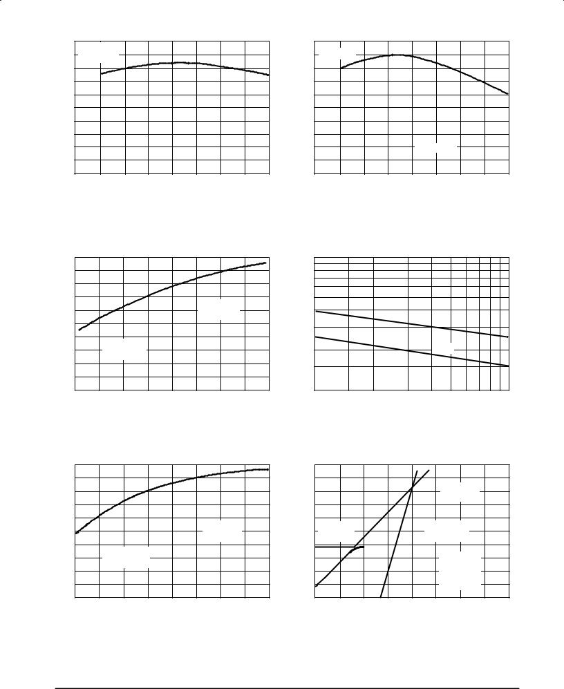
Figure 1. Typical Noise Figure and |
Figure 2. Noise Figure versus Collector Current |
Associated Gain versus Frequency |
|
MRF587 |
MOTOROLA RF DEVICE DATA |
2 |
|
(dB) |
20 |
f = 500 MHz |
|
|
|
GAIN |
|
|
|
|
|
|
VCE = 15 V |
|
|
|
|
POWER |
16 |
|
|
|
|
|
|
|
|
|
|
AVAILABLE |
12 |
|
|
|
|
8 |
|
|
|
|
|
, MAXIMUM |
|
|
|
|
|
4 |
|
|
|
|
|
|
|
|
|
|
|
Umax |
0 |
|
|
|
|
G |
50 |
100 |
150 |
200 |
|
|
0 |
IC, COLLECTOR CURRENT (mA)
Figure 3. GUmax versus Collector Current
|
6 |
|
|
|
|
(GHz) |
|
VCE = 15 V |
|
|
|
5 |
|
|
|
|
|
PRODUCT |
|
|
|
|
|
4 |
|
|
|
|
|
GAIN-BANDWIDTH |
3 |
|
|
|
|
2 |
|
|
f = 1000 MHz |
|
|
, |
|
|
|
|
|
T |
|
|
|
|
|
f |
|
|
|
|
|
|
1 |
|
100 |
150 |
200 |
|
0 |
50 |
IC, COLLECTOR CURRENT (mA)
Figure 4. Gain±Bandwidth Product versus Collector Current
|
|
|
|
|
|
TYPICAL PERFORMANCE |
|
|
|
|
|
||||
7 |
|
|
|
|
|
|
|
|
|
10 |
|
|
|
|
|
6 |
|
|
|
|
|
|
|
|
|
7 |
|
|
|
|
|
|
|
|
|
|
|
|
|
|
|
|
|
|
|
|
|
NOISENF,FIGURE (dB) |
|
|
|
|
|
VCC = 15 V |
|
|
CAPACITANCE(pF) |
5 |
|
|
Ccb |
|
|
|
|
|
|
|
|
|
2 |
|
|
|
|
||||
5 |
|
|
|
|
|
f = 300 MHz |
|
|
|
|
|
|
Cob |
|
|
|
|
|
|
|
|
|
|
|
|
3 |
|
|
|
|
|
4 |
|
|
|
|
|
|
|
|
|
|
|
|
|
|
|
|
|
CIRCUIT PER |
|
|
|
|
|
|
|
|
|
|
|
|
|
|
|
FIGURE 16 |
|
|
|
|
|
|
|
|
|
|
|
|
|
3 |
|
|
|
|
|
|
|
|
|
|
|
|
|
|
|
2 |
50 |
60 |
70 |
80 |
90 |
100 |
110 |
120 |
|
1 |
2 |
3 |
5 |
7 |
10 |
40 |
|
1 |
|||||||||||||
|
|
IC, COLLECTOR CURRENT (mA) |
|
|
|
|
VCB, COLLECTOR BASE VOLTAGE (V) |
|
|
||||||
Figure 5. Broadband Noise Figure |
Figure 6. Junction Capacitance versus Voltage |
|
80 |
|
|
|
|
|
|
|
31 |
|
|
60 |
|
|
|
|
|
|
|
|
(dBmV) |
|
|
|
|
|
|
|
|
29 |
(dBm) |
(dBm) |
|
|
|
|
|
|
|
|
|
76 |
|
|
|
|
|
|
|
27 |
50 |
|
|
|
|
|
3RD ORDER |
|
|
|||
|
|
|
|
|
|
|
|
|
|
|
|
|
|
|
|
|
||||
|
|
|
|
|
|
|
|
|
|
|
|
|
|
|
INTERCEPT |
|
|
|||
|
|
|
|
|
|
|
|
|
25 |
|
|
|
|
|
|
|
|
|
|
|
OUTPUT, VOLTAGE |
|
|
|
|
|
|
|
|
OUTPUT, POWER |
OUTPUT, POWER |
|
|
|
|
|
|
f1 = 205 MHz |
|
|
|
72 |
|
|
|
|
|
|
|
17 |
|
|
|
|
|
|
|
|
||||
|
|
|
|
|
|
|
VCC = 15 V |
|
21 |
|
|
|
+1 dB |
|
|
|
CIRCUIT PER |
|
|
|
|
|
|
|
|
|
|
f = 200 MHz |
|
|
|
|
COMP. PT. |
|
|
|
FIGURE 16 |
|
|
||
|
68 |
|
|
|
|
|
|
19 |
|
|
30 |
|
|
|
|
|
||||
|
|
CIRCUIT PER |
|
|
|
|
|
|
|
|
|
|
|
|
|
|
|
|||
|
|
|
|
|
|
|
|
|
out |
out |
|
|
|
|
|
|
|
|
|
|
out |
64 |
|
FIGURE 16 |
|
|
|
|
|
15 |
20 |
|
|
|
|
|
f2 = 211 MHz |
|
|
||
V |
|
|
|
|
|
|
|
P |
P |
|
|
|
|
|
VCC = 15 V |
|
|
|||
|
|
|
|
|
|
|
|
|
13 |
|
|
|
|
|
|
|
|
|
|
|
|
60 |
|
|
|
|
|
|
|
|
|
|
|
|
|
|
|
IC = 90 mA |
|
|
|
|
50 |
60 |
70 |
80 |
90 |
100 |
110 |
11 |
|
|
10 |
10 |
20 |
30 |
40 |
50 |
60 |
70 |
80 |
|
|
40 |
120 |
|
|
0 |
|||||||||||||||
|
|
|
IC, COLLECTOR CURRENT (mA) |
|
|
|
|
|
|
|
Pin, INPUT POWER (dBm) |
|
|
|||||||
Figure 7. 1.0 dB Compression Point versus |
Figure 8. Third Order Intercept Point |
Collector Current
MOTOROLA RF DEVICE DATA |
MRF587 |
|
3 |

TYPICAL PERFORMANCE (continued)
|
± 48 |
|
|
|
|
|
|
|
|
|
|
VCE = 15 V |
|
|
|
|
|
|
|
|
± 52 |
PRef = 50 dBmV |
|
|
|
|
CHR |
|
|
|
|
|
CIRCUIT PER |
|
|
|
|
||
(dB) |
|
|
|
|
|
|
|
|
|
|
|
|
FIGURE 16 |
|
|
|
CH13 |
|
|
IMD, DISTORTION |
± 56 |
|
|
TEST PER FIGURE 17 |
|
|
|
||
|
|
|
|
|
|
|
|||
± 60 |
|
|
|
|
|
|
|
|
|
± 64 |
|
|
|
|
|
|
|
|
|
|
|
|
|
|
|
|
|
|
|
|
|
|
|
|
|
|
|
CH2 |
|
|
40 |
50 |
60 |
70 |
80 |
90 |
100 |
110 |
120 |
|
± 60 |
|
|
|
|
|
|
|
|
VCC = 15 V |
|
|
|
|
± 64 |
|
PRef = 50 dBmV @ 200 MHz |
|
||
|
|
|
|
CIRCUIT PER |
|
|
|
|
|
|
|
|
|
(dB) |
|
|
|
|
FIGURE 16 |
|
± 68 |
|
|
|
|
|
|
, DISTORTION |
|
|
|
|
|
|
± 72 |
|
|
|
|
|
|
|
|
|
|
|
|
|
3 |
|
|
|
|
|
|
TB |
± 76 |
|
TEST PER FIGURE 18 |
|
||
|
|
|
||||
|
± 80 |
80 |
90 |
100 |
110 |
120 |
|
70 |
|||||
IC, COLLECTOR CURRENT (mA) |
IC, COLLECTOR CURRENT (mA) |
Figure 9. Second Order Distortion versus |
Figure 10. Triple Beat Distortion versus |
Collector Current |
Collector Current |
|
± 10 |
|
|
|
|
|
|
|
|
140 |
|
|
|
|
|
|
|
|
|
|
|
|
|
|
VCC = 15 V |
|
|
μV) |
|
|
VCC = 15 V |
|
|
|
|
|
|
|
± 20 |
|
|
|
|
|
|
130 |
|
|
|
|
|
|
|
|
||
DISTORTION(dB) |
|
|
|
|
PRef = 50 dBmV |
|
VOLTAGE(dB |
|
|
|
|
|
|
|
|
|||
|
|
|
|
|
|
|
|
|
|
|
|
|
|
|
||||
± 30 |
|
|
|
|
|
|
|
120 |
|
|
|
|
|
|
|
|
||
|
|
|
|
|
|
|
|
|
|
|
|
|
|
|
|
|
||
35 |
|
|
|
|
|
CH13 |
|
|
OUTPUT |
|
|
|
|
|
|
|
|
|
± 40 |
CIRCUIT PER |
|
|
|
|
|
110 |
|
|
|
|
CIRCUIT PER |
|
|
||||
, |
|
|
|
|
|
|
|
|
|
|
|
|
||||||
FIGURE 16 |
|
|
|
|
|
|
|
|
|
|
FIGURE 16 |
|
|
|||||
XMD |
± 50 |
|
|
|
|
|
Ref |
100 |
|
|
|
|
|
|
||||
TEST PER FIGURE 19 |
|
|
|
|
|
|
|
|
TEST PER FIGURE 20 |
|
||||||||
|
|
|
|
|
|
, |
|
|
|
|
|
|
||||||
|
|
|
|
|
|
|
|
|
V |
|
|
|
|
|
|
|
|
|
|
± 60 |
|
|
|
|
|
|
110 |
120 |
90 |
|
|
|
80 |
90 |
100 |
110 |
120 |
|
40 |
50 |
60 |
70 |
80 |
90 |
100 |
40 |
50 |
60 |
70 |
|||||||
|
|
|
IC, COLLECTOR CURRENT (mA) |
|
|
|
|
IC, COLLECTOR CURRENT (mA) |
|
|
||||||||
Figure 11. 35±Channel X±Modulation Distortion |
Figure 12. DIN 45004B versus Collector Current |
versus Collector Current
MRF587 |
MOTOROLA RF DEVICE DATA |
4 |
|

|
|
|
+ j50 |
|
|
|
VCE = 15 V |
IC = 90 mA |
|
|
|
90° |
|
|
|
|
|
|
|
|
|
|
|
|
|
° |
|
|
|
|
60° |
|
|||
|
+ j25 |
|
|
|
|
+ j100 |
|
|
120 |
f = 0.1 GHz |
|
|
|
|
|
||
|
|
|
|
|
|
|
|
|
|
|
|
|
|||||
|
|
|
|
|
|
|
|
|
|
|
|
|
|
|
|||
|
|
|
|
|
|
|
+ j150 |
150° |
|
|
S21 |
0.2 |
|
|
|
|
30° |
|
|
|
|
|
|
|
|
|
|
|
|
|
|
|
|||
|
|
|
|
|
|
|
|
|
|
|
0.8 |
|
|
|
|
||
+ j10 |
|
|
|
|
|
|
+ j250 |
|
|
|
|
|
1 |
|
|
|
|
|
|
|
|
|
|
|
|
|
|
0.4 |
|
|
|
|
|||
|
|
|
|
|
|
|
|
|
|
|
0.6 |
|
|
|
|||
|
|
|
|
|
|
|
|
|
|
|
|
|
|
S12 |
|
||
|
|
|
|
|
|
|
+ j500 |
|
|
|
|
0.6 |
|
|
|
||
|
1 |
|
|
|
|
|
|
|
|
|
1 |
0.4 |
|
|
|
|
|
S11 |
|
|
|
|
|
|
180° 25 |
|
|
|
f = 0.1 GHz |
|
|
0.5 0° |
|||
10 0.8 |
25 |
50 |
100 |
150 |
250 |
500 |
20 |
15 |
10 |
5 |
0.1 |
0.2 |
0.3 |
0.4 |
|||
0 |
0.6 |
|
|
|
|
|
|
|
|
|
|
|
|
|
|
|
|
|
|
|
|
|
|
|
|
|
|
|
|
|
|
|
|
|
|
|
0.4 |
0.6 |
0.4 |
|
|
|
± j500 |
|
|
|
|
|
|
|
|
|
|
|
0.2 |
0.2 |
f = 0.1 GHz |
± j250 |
|
|
|
|
|
|
|
|
|
|
|||
± j10 |
f = 0.1 GHz |
0.8 |
° |
|
|
|
|
|
|
|
|
± 30° |
|||||
|
|
|
1 |
|
|
|
|
±150 |
|
|
|
|
|
|
|
|
|
|
|
|
|
S22 |
|
|
± j150 |
|
|
|
|
|
|
|
|
|
|
|
|
|
|
|
|
|
|
|
|
|
|
|
|
|
|
|
|
|
± j25 |
|
|
|
|
± j100 |
|
|
±120° |
|
|
|
|
± 60° |
|
||
|
|
|
|
|
|
|
|
± 90° |
|
|
|
|
|||||
|
|
|
|
|
|
|
|
|
|
|
|
|
|
|
|||
|
|
|
|
|
|
|
|
|
|
|
|
|
|
|
|
||
|
|
|
± j50 |
|
|
|
|
|
|
|
|
|
|
|
|
|
|
Figure 13. Input/Output Reflection |
|
|
|
|
Figure 14. Forward/Reverse Transmission |
||||||||||
Coefficient versus Frequency (GHz) |
|
|
|
|
Coefficients versus Frequency (GHz) |
||||||||||
|
|
|
|
|
|
|
|
|
|
|
|
|
|
|
|
VCE |
IC |
f |
S |
11 |
|
|
S |
21 |
|
|
S12 |
|
S22 |
||
(Volts) |
(mA) |
(MHz) |
|S11| |
|
± φ |
|S21| |
|
± φ |
|
|S12| |
|
± φ |
|S22| |
|
± φ |
5.0 |
30 |
100 |
0.56 |
|
± 131 |
16.45 |
|
113 |
|
0.04 |
|
45 |
0.49 |
|
± 91 |
|
|
200 |
0.58 |
|
± 159 |
9.42 |
|
98 |
|
0.06 |
|
49 |
0.38 |
|
± 116 |
|
|
400 |
0.60 |
|
± 178 |
5.00 |
|
86 |
|
0.08 |
|
55 |
0.35 |
|
± 132 |
|
|
600 |
0.64 |
|
170 |
3.61 |
|
76 |
|
0.11 |
|
56 |
0.38 |
|
± 138 |
|
|
800 |
0.67 |
|
162 |
2.92 |
|
67 |
|
0.14 |
|
55 |
0.41 |
|
± 144 |
|
|
1000 |
0.70 |
|
155 |
2.55 |
|
58 |
|
0.17 |
|
54 |
0.44 |
|
± 152 |
|
|
|
|
|
|
|
|
|
|
|
|
|
|
|
|
|
60 |
100 |
0.53 |
|
± 141 |
17.89 |
|
110 |
|
0.04 |
|
50 |
0.47 |
|
± 102 |
|
|
200 |
0.56 |
|
± 164 |
10.05 |
|
97 |
|
0.05 |
|
55 |
0.39 |
|
± 126 |
|
|
400 |
0.59 |
|
178 |
5.31 |
|
85 |
|
0.09 |
|
60 |
0.38 |
|
± 141 |
|
|
600 |
0.63 |
|
169 |
3.82 |
|
76 |
|
0.12 |
|
59 |
0.40 |
|
± 146 |
|
|
800 |
0.66 |
|
161 |
3.09 |
|
67 |
|
0.15 |
|
57 |
0.44 |
|
± 153 |
|
|
1000 |
0.69 |
|
155 |
2.67 |
|
58 |
|
0.18 |
|
55 |
0.47 |
|
± 160 |
|
|
|
|
|
|
|
|
|
|
|
|
|
|
|
|
|
90 |
100 |
0.52 |
|
± 145 |
18.26 |
|
109 |
|
0.04 |
|
52 |
0.47 |
|
± 106 |
|
|
200 |
0.56 |
|
± 166 |
10.20 |
|
96 |
|
0.05 |
|
57 |
0.39 |
|
± 130 |
|
|
400 |
0.59 |
|
177 |
5.38 |
|
85 |
|
0.09 |
|
62 |
0.39 |
|
± 144 |
|
|
600 |
0.63 |
|
168 |
3.86 |
|
76 |
|
0.12 |
|
60 |
0.41 |
|
± 149 |
|
|
800 |
0.66 |
|
161 |
3.12 |
|
67 |
|
0.15 |
|
58 |
0.45 |
|
± 155 |
|
|
1000 |
0.69 |
|
155 |
2.70 |
|
58 |
|
0.19 |
|
55 |
0.48 |
|
± 162 |
|
|
|
|
|
|
|
|
|
|
|
|
|
|
|
|
10 |
30 |
100 |
0.53 |
|
± 122 |
18.36 |
|
115 |
|
0.04 |
|
48 |
0.50 |
|
± 75 |
|
|
200 |
0.53 |
|
± 153 |
10.63 |
|
100 |
|
0.05 |
|
51 |
0.36 |
|
± 96 |
|
|
400 |
0.55 |
|
175 |
5.71 |
|
87 |
|
0.08 |
|
57 |
0.33 |
|
± 112 |
|
|
600 |
0.59 |
|
173 |
4.16 |
|
78 |
|
0.10 |
|
58 |
0.35 |
|
± 119 |
|
|
800 |
0.62 |
|
165 |
3.37 |
|
68 |
|
0.13 |
|
57 |
0.39 |
|
± 127 |
|
|
1000 |
0.65 |
|
158 |
2.95 |
|
59 |
|
0.15 |
|
55 |
0.42 |
|
± 136 |
|
|
|
|
|
|
|
|
|
|
|
|
|
|
|
|
|
60 |
100 |
0.49 |
|
± 132 |
20.19 |
|
112 |
|
0.03 |
|
51 |
0.46 |
|
± 85 |
|
|
200 |
0.51 |
|
± 158 |
11.54 |
|
99 |
|
0.05 |
|
57 |
0.35 |
|
± 107 |
|
|
400 |
0.53 |
|
± 178 |
6.12 |
|
87 |
|
0.08 |
|
61 |
0.33 |
|
± 123 |
|
|
600 |
0.58 |
|
171 |
4.43 |
|
78 |
|
0.11 |
|
60 |
0.36 |
|
± 129 |
|
|
800 |
0.60 |
|
164 |
3.58 |
|
68 |
|
0.14 |
|
59 |
0.40 |
|
± 136 |
|
|
1000 |
0.63 |
|
157 |
3.12 |
|
60 |
|
0.16 |
|
57 |
0.44 |
|
± 144 |
|
|
|
|
|
|
|
|
|
|
|
|
|
|
|
|
|
90 |
100 |
0.48 |
|
± 135 |
20.82 |
|
111 |
|
0.03 |
|
53 |
0.45 |
|
± 88 |
|
|
200 |
0.50 |
|
± 160 |
11.77 |
|
98 |
|
0.05 |
|
59 |
0.34 |
|
± 111 |
|
|
400 |
0.53 |
|
± 179 |
6.22 |
|
86 |
|
0.08 |
|
63 |
0.33 |
|
± 126 |
|
|
600 |
0.57 |
|
171 |
4.50 |
|
78 |
|
0.11 |
|
62 |
0.36 |
|
± 131 |
|
|
800 |
0.60 |
|
164 |
3.64 |
|
68 |
|
0.14 |
|
59 |
0.41 |
|
± 139 |
|
|
1000 |
0.63 |
|
157 |
3.18 |
|
60 |
|
0.17 |
|
57 |
0.44 |
|
± 147 |
|
|
|
|
|
|
|
|
|
|
|
|
|
|
|
(continued) |
|
|
|
Table 1. Common±Emitter S±Parameters |
|
|
|
|
|
|||||||
|
|
|
|
|
|
|
|
|
|
|
|
|
|
|
|
MOTOROLA RF DEVICE DATA |
|
|
|
|
|
|
|
|
|
|
|
|
MRF587 |
||
|
|
|
|
|
|
|
|
|
|
|
|
|
|
5 |
|

VCE |
IC |
f |
|
S |
11 |
|
S21 |
|
S12 |
|
S22 |
|||
(Volts) |
(mA) |
(MHz) |
|S11| |
|
± f |
|S21| |
|
± f |
|S12| |
|
± f |
|S22| |
|
± f |
15 |
30 |
100 |
0.49 |
|
± 112 |
20.34 |
|
118 |
0.04 |
|
54 |
0.51 |
|
± 52 |
|
|
200 |
0.52 |
|
± 145 |
11.51 |
|
101 |
0.05 |
|
56 |
0.36 |
|
± 77 |
|
|
400 |
0.48 |
|
± 164 |
6.12 |
|
87 |
0.09 |
|
63 |
0.32 |
|
± 74 |
|
|
600 |
0.52 |
|
± 174 |
4.19 |
|
75 |
0.12 |
|
62 |
0.32 |
|
± 90 |
|
|
800 |
0.53 |
|
177 |
3.29 |
|
68 |
0.16 |
|
61 |
0.38 |
|
± 90 |
|
|
1000 |
0.53 |
|
168 |
2.76 |
|
61 |
0.20 |
|
56 |
0.47 |
|
± 90 |
|
|
|
|
|
|
|
|
|
|
|
|
|
|
|
|
60 |
100 |
0.45 |
|
± 122 |
22.14 |
|
115 |
0.03 |
|
56 |
0.45 |
|
± 60 |
|
|
200 |
0.49 |
|
± 150 |
12.24 |
|
99 |
0.05 |
|
60 |
0.33 |
|
± 86 |
|
|
400 |
0.45 |
|
± 166 |
6.45 |
|
86 |
0.09 |
|
65 |
0.30 |
|
± 83 |
|
|
600 |
0.50 |
|
± 175 |
4.42 |
|
75 |
0.13 |
|
63 |
0.32 |
|
± 99 |
|
|
800 |
0.51 |
|
177 |
3.47 |
|
68 |
0.16 |
|
61 |
0.38 |
|
± 98 |
|
|
1000 |
0.51 |
|
168 |
2.91 |
|
62 |
0.20 |
|
55 |
0.46 |
|
± 96 |
|
|
|
|
|
|
|
|
|
|
|
|
|
|
|
|
90 |
100 |
0.44 |
|
± 127 |
22.76 |
|
114 |
0.03 |
|
58 |
0.43 |
|
± 62 |
|
|
200 |
0.48 |
|
± 152 |
12.44 |
|
98 |
0.05 |
|
62 |
0.32 |
|
± 89 |
|
|
400 |
0.44 |
|
± 167 |
6.55 |
|
85 |
0.09 |
|
66 |
0.29 |
|
± 85 |
|
|
600 |
0.50 |
|
± 176 |
4.47 |
|
75 |
0.13 |
|
64 |
0.32 |
|
± 102 |
|
|
800 |
0.51 |
|
176 |
3.51 |
|
69 |
0.17 |
|
61 |
0.38 |
|
± 100 |
|
|
1000 |
0.51 |
|
168 |
2.95 |
|
62 |
0.20 |
|
55 |
0.46 |
|
± 98 |
|
|
|
|
|
|
|
|
|
|
|
|
|
|
|
Table 1. Common±Emitter S±Parameters (continued)
|
R1 |
+ |
VBB |
Y3 |
|
C5 |
C7 |
|
TL3 |
 C3
C3
TL1
RF |
|
INPUT Y1 |
C1 |
|
3.12 cm
C10 
RFC1
VCC
Y4 +
C8 |
C6 |
|
TL4 |
|
|
3.68 cm |
|
|
C9 |
C4 |
DUT |
TL2 |
|
|
|
|
RF |
C2 |
Y2 OUTPUT |
|
C1, C2 |
Ð 470 pF Chip (Ceramic) |
R1 Ð 2.7 k W, 1±1/2 W |
||||
C3, C4 Ð 0.018 mF Chip Capacitor |
RFC1 Ð 0.15 mH Molded Choke |
|||||
C5, C6 Ð 0.1 |
mF Mylar |
TL1, TL2 Ð Z o = 26 W, 0.0625 TFG as shown in |
||||
C7, C8 |
Ð 1.0 |
mF, 25 Vdc Electrolytic |
TL1, TL2 Photomaster |
|||
C9 |
Ð 91 pF Mini±Unelco (C9 Taped 3.68 cm from |
TL3, TL4 Ð l/4 Microstrip, Zo = 100 W |
||||
C9 |
Ð Collector Connection on TL4 as shown) |
Y1, Y2 |
Ð N±Type Connection (Female) |
|||
C10 |
Ð 35± 45 pF Johanson Ceramic Capacitor, JMC |
Y3, Y4 |
Ð BNC±Type Connector (Female) |
|||
C10 |
Ð |
5801 or Equivalent (C10 Taped 3.12 cm from |
Board Material Ð 0.0625 ″ Thick Glass Teflon er = 2.5 |
|||
C10 |
Ð Base Connection on TL1) |
|
|
|||
Figure 15. Narrowband Test Fixture Schematic
500 MHz
MRF587 |
MOTOROLA RF DEVICE DATA |
6 |
|

VBB |
VCC |
C4 |
C5 |
VCC = 15 V
Pg = 11 dB
f = 5 ± 375 MHz
Zo = 75 Ω
R2
RF
OUTPUT
|
|
T2 |
|
C3 |
R3 |
|
C6 |
|
|
DUT |
C7 |
RF |
|
T1 |
|
|
|
|
|
INPUT |
|
|
|
L1 |
|
|
|
|
C2 |
|
|
C1 |
|
R1 |
C8 |
C1, C7 Ð 0.5± 10 pF |
R1 Ð 12 Ω 1.0 W (2.0± 24 Ω on each emitter port) |
||
C2, C6 Ð 0.001 |
μF |
R2 Ð 1.8 k 1/8 W |
|
C3 Ð 0.01 μF |
|
R3 Ð 2.2 k 1/8 W |
|
C4, C5 Ð 0.01 |
μF Feedthru |
L1 Ð 1 Turn 0.012 dia #22 AWG |
|
C8 Ð 12 pF |
|
T1(1) Ð 5 Turns Tapped at 2 Turns, #30 AWG |
|
|
|
T2(1) Ð 8 Turns Tapped at 3 Turns, #30 AWG |
|
(1) Ferroxcube 135 CT050 3D3 Material
Figure 16. Broadband Test Circuit Schematic
|
PRef |
|
|
|
|
|
DISTORTION |
f2 ± f1 |
f1 |
f2 |
f1 + f2 |
Figure 17. Second Order Distortion Test
DISTORTION |
UNMODULATED |
|
CARRIER |
||
PRef |
||
|
||
|
100% |
|
|
MODULATION |
|
|
15 kHz |
Figure 19. Cross Modulation Distortion Test
PRef |
|
|
|
DISTORTION |
|
f1 |
f2 |
f3 |
Figure 18. Triple Beat Distortion Test
VRef |
|
± 6 dB |
|
|
|
199 MHz |
± 60 dB |
|
|
|
|
|
211 MHz |
217 MHz |
f1 |
f2 |
f3 |
193 MHz |
205 MHz |
|
|
|
Figure 20. DIN 45004B Intermodulation Test
MOTOROLA RF DEVICE DATA |
MRF587 |
|
7 |

PACKAGE DIMENSIONS
|
|
2 |
|
D |
|
|
|
|
|
|
|
|
1 |
|
|
|
MILLIMETERS |
INCHES |
|||
|
|
4 |
|
|
|
|||||
|
|
|
|
|
|
|||||
|
|
|
|
|
DIM |
MIN |
MAX |
MIN |
MAX |
|
|
|
3 |
|
|
|
|||||
|
|
|
|
|
A |
7.06 |
7.26 |
0.278 |
0.286 |
|
|
|
|
K |
|
|
|||||
|
|
|
|
|
B |
6.20 |
6.50 |
0.244 |
0.256 |
|
|
|
|
M |
|
|
C |
15.24 |
16.51 |
0.600 |
0.650 |
|
|
|
|
|
|
D |
0.66 |
0.86 |
0.026 |
0.034 |
|
|
|
|
|
|
E |
1.40 |
1.65 |
0.055 |
0.065 |
T |
|
A |
|
|
|
F |
1.52 |
Ð |
0.060 |
Ð |
|
J |
|
|
J |
0.10 |
0.15 |
0.004 |
0.006 |
||
|
|
|
|
|
K |
11.17 |
Ð |
0.440 |
Ð |
|
|
|
|
|
|
|
M |
45° NOM |
45° NOM |
||
|
|
|
|
S |
|
P |
Ð |
1.27 |
Ð |
0.050 |
|
|
|
|
|
S |
2.74 |
3.35 |
0.108 |
0.132 |
|
|
|
|
|
|
|
|||||
F |
|
|
SEATING |
|
C |
T |
1.40 |
1.78 |
0.055 |
0.070 |
P |
|
PLANE |
|
U |
2.92 |
3.68 |
0.115 |
0.145 |
||
|
|
|
||||||||
|
|
|
|
|
|
|
|
|
|
|
8±32 NC 2A |
|
|
|
|
|
|
|
STYLE 1: |
|
WRENCH FLAT |
|
E |
PIN 1. |
EMITTER |
|
B |
U |
2. |
BASE |
|
|
3. |
EMITTER |
|
|
|
|
4. |
COLLECTOR |
CASE 244A±01
ISSUE A
Motorola reserves the right to make changes without further notice to any products herein. Motorola makes no warranty, representation or guarantee regarding the suitability of its products for any particular purpose, nor does Motorola assume any liability arising out of the application or use of any product or circuit, and specifically disclaims any and all liability, including without limitation consequential or incidental damages. ªTypicalº parameters can and do vary in different applications. All operating parameters, including ªTypicalsº must be validated for each customer application by customer's technical experts. Motorola does not convey any license under its patent rights nor the rights of others. Motorola products are not designed, intended, or authorized for use as components in systems intended for surgical implant into the body, or other applications intended to support or sustain life, or for any other application in which the failure of the Motorola product could create a situation where personal injury or death may occur. Should Buyer purchase or use Motorola products for any such unintended or unauthorized application, Buyer shall indemnify and hold Motorola and its officers, employees, subsidiaries, affiliates, and distributors harmless against all claims, costs, damages, and expenses, and reasonable attorney fees arising out of, directly or indirectly, any claim of personal injury or death associated with such unintended or unauthorized use, even if such claim alleges that Motorola was negligent regarding the design or manufacture of the part. Motorola and  are registered trademarks of Motorola, Inc. Motorola, Inc. is an Equal Opportunity/Affirmative Action Employer.
Literature Distribution Centers:
USA: Motorola Literature Distribution; P.O. Box 20912; Phoenix, Arizona 85036.
EUROPE: Motorola Ltd.; European Literature Centre; 88 Tanners Drive, Blakelands, Milton Keynes, MK14 5BP, England. JAPAN: Nippon Motorola Ltd.; 4-32-1, Nishi-Gotanda, Shinagawa-ku, Tokyo 141, Japan.
ASIA PACIFIC: Motorola Semiconductors H.K. Ltd.; Silicon Harbour Center, No. 2 Dai King Street, Tai Po Industrial Estate, Tai Po, N.T., Hong Kong.
◊ |
MRF587/D |
|
*MRF587/D* |