

MOTOROLA
SEMICONDUCTOR TECHNICAL DATA
Order this document by MRF182/D
The RF MOSFET Line |
|
|
|
|
|
|
|
|
|
|
|
|
|
|
RF Power |
|
|
|
MRF182 |
||||||||||
Field Effect Transistors |
|
|
|
MRF182S |
||||||||||
N±Channel Enhancement±Mode Lateral |
|
|
|
|
|
|
|
|
|
|
|
|
|
|
MOSFETs |
|
|
|
|
|
|
|
|
|
|
|
|
|
|
• High Gain, Rugged Device |
|
|
|
|
|
|
|
|
|
|
|
|
|
|
|
|
|
|
|
30 W, 1.0 GHz |
|||||||||
• Broadband Performance from HF to 1 GHz |
|
|
|
|
|
|||||||||
• Bottom Side Source Eliminates DC Isolators, Reducing Common |
|
|
|
LATERAL N±CHANNEL |
||||||||||
|
|
|
|
|
BROADBAND |
|||||||||
Mode Inductances |
|
|
|
|
|
|||||||||
|
|
|
RF POWER MOSFETs |
|||||||||||
|
|
|
|
|
||||||||||
|
|
|
|
|
|
|
|
|
|
|
|
|
|
|
|
|
D |
||||||||||||
|
|
|
|
|
|
|
|
|
|
|
|
|
|
|
|
|
|
|
|
|
|
|
|
|
|
|
|
|
|
|
|
|
|
|
|
|
|
|
|
|
|
|
|
|
|
|
|
|
|
|
|
|
|
|
|
|
|
|
|
|
|
|
|
|
|
|
|
|
|
|
|
|
|
|
|
|
|
|
|
|
|
|
|
|
|
|
|
|
|
|
|
|
|
|
|
|
|
|
|
|
|
|
|
|
G |
CASE 360B±01, STYLE 1 |
|
(MRF182) |
||
|
||
|
S |
|
|
CASE 360C±03, STYLE 1 |
|
MAXIMUM RATINGS |
(MRF182S) |
|
|
Rating |
Symbol |
Value |
Unit |
|
|
|
|
Drain±Source Voltage |
VDSS |
65 |
Vdc |
Gate±Source Voltage |
VGS |
± 20 |
Vdc |
Total Device Dissipation @ TC = 70°C |
PD |
74 |
W |
Derate above 70°C |
|
0.57 |
W/°C |
|
|
|
|
Storage Temperature Range |
Tstg |
± 65 to +150 |
°C |
Operating Junction Temperature |
TJ |
200 |
°C |
THERMAL CHARACTERISTICS |
|
|
|
|
|
|
|
Characteristic |
Symbol |
Max |
Unit |
|
|
|
|
Thermal Resistance, Junction to Case |
RθJC |
1.75 |
°C/W |
ELECTRICAL CHARACTERISTICS (TC = 25°C unless otherwise noted)
Characteristic |
Symbol |
Min |
Typ |
Max |
Unit |
|
|
|
|
|
|
OFF CHARACTERISTICS
Drain±Source Breakdown Voltage |
V(BR)DSS |
65 |
± |
± |
Vdc |
(VGS = 0, ID = 1.0 mAdc) |
|
|
|
|
|
Zero Gate Voltage Drain Current |
IDSS |
± |
± |
1 |
μAdc |
(VDS = 28 V, VGS = 0) |
|
|
|
|
|
Gate±Source Leakage Current |
IGSS |
± |
± |
1 |
μAdc |
(VGS = 20 V, VDS = 0) |
|
|
|
|
|
NOTE ± CAUTION ± MOS devices are susceptible to damage from electrostatic charge. Reasonable precautions in handling and packaging MOS devices should be observed.
REV 5
MOTOROLAMotorola, Inc. 1997RF DEVICE DATA |
MRF182 |
|
1 |

ELECTRICAL CHARACTERISTICS ± continued (TC = 25°C unless otherwise noted)
Characteristic |
Symbol |
Min |
Typ |
Max |
Unit |
|
|
|
|
|
|
ON CHARACTERISTICS
Gate Threshold Voltage |
VGS(th) |
2 |
|
3 |
4 |
|
Vdc |
(VDS = 10 V, ID = 100 μA) |
|
|
|
|
|
|
|
Gate Quiescent Voltage |
VGS(Q) |
3 |
|
4 |
5 |
|
Vdc |
(VDS = 28 V, ID = 50 mA) |
|
|
|
|
|
|
|
Drain±Source On±Voltage |
VDS(on) |
± |
|
0.9 |
1.2 |
|
Vdc |
(VGS = 10 V, ID = 3 A) |
|
|
|
|
|
|
|
Forward Transconductance |
gfs |
1.6 |
|
1.8 |
± |
|
S |
(VDS = 10 V, ID = 3 A) |
|
|
|
|
|
|
|
DYNAMIC CHARACTERISTICS |
|
|
|
|
|
|
|
|
|
|
|
|
|
|
|
Input Capacitance |
Ciss |
± |
|
56 |
± |
|
pF |
(VDS = 28 V, VGS = 0, f = 1 MHz) |
|
|
|
|
|
|
|
Output Capacitance |
Coss |
± |
|
28 |
± |
|
pF |
(VDS = 28 V, VGS = 0, f = 1 MHz) |
|
|
|
|
|
|
|
Reverse Transfer Capacitance |
Crss |
± |
|
2.5 |
± |
|
pF |
(VDS = 28 V, VGS = 0, f = 1 MHz) |
|
|
|
|
|
|
|
FUNCTIONAL CHARACTERISTICS |
|
|
|
|
|
|
|
|
|
|
|
|
|
|
|
Common Source Power Gain |
Gps |
11 |
|
14 |
± |
|
dB |
(VDD = 28 Vdc, Pout = 30 W, IDQ = 50 mA, f = 945 MHz) |
|
|
|
|
|
|
|
Drain Efficiency |
η |
50 |
|
60 |
± |
|
% |
(VDD = 28 Vdc, Pout = 30 W, IDQ = 50 mA, f = 945 MHz) |
|
|
|
|
|
|
|
Load Mismatch |
|
|
|
|
|
|
|
(VDD = 28 Vdc, Pout = 30 W, IDQ = 50 mA, f = 945 MHz, |
Ψ |
|
No Degradation in Output Power |
|
|||
Load VSWR 5:1 at All Phase Angles) |
|
|
|
|
|
|
|
|
|
|
|
|
|
|
|
Series Equivalent Input Impedance |
Zin |
± |
|
0.81 + j1.6 |
± |
|
ohms |
(VDD = 28 Vdc, Pout = 30 W, IDQ = 50 mA, f = 960 MHz) |
|
|
|
|
|
|
|
Series Equivalent Output Impedance |
Zout |
± |
|
2.15 ± j1.7 |
± |
|
ohms |
(VDD = 28 Vdc, Pout = 30 W, IDQ = 50 mA, f = 960 MHz) |
|
|
|
|
|
|
|
MRF182 |
MOTOROLA RF DEVICE DATA |
2 |
|

R1 |
|
C6 |
C7 |
R4 |
|
VGG |
|
|
|
C11 |
C12 |
|
|
|
C8 |
||
R2 |
C5 |
|
|
VDD |
|
|
|
|
C9 |
B1 |
|
|
|
R3 |
C2 |
L1 |
C13 |
|
|
|
C10 |
RF |
|
DUT |
|
|
|
|
|
|
|
|
|
INPUT |
C1 |
|
C4 |
|
RF |
|
TL2 |
|
|
|
|
|
TL3 |
|
|
OUTPUT |
|
|
TL1 |
|
TL4 |
||
|
|
|
|
C3 |
C14 |
|
B1 |
Short RF Bead Fair Rite±274301944 |
L1 |
5 Turns, 20 AWG, IDIA 0.126 |
C1 |
18 pF Chip Capacitor |
R1 |
10 kW, 1/4 W Resistor |
C2, C3, C6, C9 |
43 pF Chip Capacitor |
R2 |
13 kW, 1/4 W Resistor |
C4 |
100 pF Chip Capacitor |
R3 |
1.0 kW, 1/4 W Chip Resistor |
C5, C12 |
10 mF, 50 Vdc Electrolytic Capacitor |
R4 |
4 x 39 W, 1/8 W Chip Resistor |
C7, C10 |
1000 pF Chip Capacitor |
″ TL1±TL4 |
Microstrip Line See Photomaster |
C8, C11 |
0.1 mF, 50 Vdc Chip Capacitor |
Ckt Board |
1/32″ Glass Teflon, er = 2.55 |
C13 |
250 mF, 50 Vdc Electrolytic Capacitor |
|
ARLON±GX±0300±55±22 |
C14 |
0.6±4.5 pF Variable Capacitor |
|
|
Figure 1. MRF182 Schematic
MOTOROLA RF DEVICE DATA |
MRF182 |
|
3 |
TYPICAL CHARACTERISTICS
|
40 |
|
|
|
|
|
|
|
|
|
|
|
|
|
VDS = 28 Vdc |
|
|
|
|
|
|
|
|
|
|
|
35 |
|
|
|
|
|
|
|
|
|
|
|
(WATTS) |
|
IDQ = 50 mA |
|
|
|
|
|
|
|
|
|
|
30 |
|
f = 1 GHz |
|
|
|
|
|
|
|
|
|
|
|
|
|
|
|
|
|
|
|
|
|
||
POWER |
|
|
|
|
|
|
|
|
|
|
|
|
|
|
|
|
|
|
|
|
|
|
|
||
25 |
|
|
|
|
|
|
|
|
|
|
|
|
|
|
|
|
|
|
|
|
|
|
|
|
|
OUTPUT, |
20 |
|
|
|
|
|
|
|
|
|
|
|
|
|
|
|
|
|
|
|
|
|
|
||
15 |
|
|
|
|
|
|
|
|
|
|
|
|
|
|
|
|
|
|
|
|
|
|
|
|
|
out |
10 |
|
|
|
|
|
|
|
|
|
|
|
|
|
|
|
|
|
|
|
|
|
|
||
|
|
|
|
|
|
|
|
|
|
|
|
|
P |
5 |
|
|
|
|
|
|
|
|
|
|
|
|
|
|
|
|
|
|
|
|
|
|
|
|
|
|
|
|
|
|
|
|
|
|
|
|
|
|
0 |
|
|
|
|
|
|
|
|
|
|
|
|
|
0.5 |
1 |
1.5 |
2 |
2.5 |
||||||
|
0 |
|||||||||||
Pin, INPUT POWER (WATTS)
Figure 2. Output Power versus
Input Power at 1 GHz
|
60 |
|
|
|
|
|
|
|
|
|
|
|
|
|
|
|
|
|
VDS = |
28 Vdc |
|
|
|
|
|
|
|
|
|
|
|
|
|
|
|
|
|
|
|
|
|
|
|
|
|
|
|
|
|
|
|
||
|
50 |
IDQ = |
50 mA |
|
|
|
|
|
|
|
|
|
|
|
|
|
|
(%) |
f = 1 GHz |
|
|
|
|
|
|
|
|
|
|
|
|
|
|
||
|
|
|
|
|
|
|
|
|
|
|
|
|
|
|
|||
20 |
|
|
|
|
|
|
|
|
|
|
|
|
|
|
|
|
|
EFFICIENCYDRAIN |
|
|
|
|
|
|
|
|
|
|
|
|
|
|
|
|
|
|
40 |
|
|
|
|
|
|
|
|
|
|
|
|
|
|
|
|
, |
30 |
|
|
|
|
|
|
|
|
|
|
|
|
|
|
|
|
|
|
|
|
|
|
|
|
|
|
|
|
|
|
|
|
|
|
|
|
|
|
|
|
|
|
|
|
|
|
|
|
|
|
|
|
d |
|
|
|
|
|
|
|
|
|
|
|
|
|
|
|
|
|
η |
|
|
|
|
|
|
|
|
|
|
|
|
|
|
|
|
|
|
10 |
|
|
|
|
|
|
|
|
|
|
|
|
|
|
|
|
|
|
|
|
|
|
|
|
|
|
|
|
|
|
|
|
|
|
|
0 |
|
|
|
|
|
|
|
|
|
|
|
|
|
|
|
|
|
5 |
10 |
15 |
20 |
25 |
30 |
35 |
40 |
|||||||||
|
0 |
||||||||||||||||
Pout, OUTPUT POWER (WATTS)
Figure 4. Drain Efficiency versus
Output Power at 1 GHz
|
16 |
|
14 |
(dB) |
12 |
|
|
GAIN |
10 |
POWER, |
6 |
|
8 |
ps |
|
G |
4 |
|
VDS = 28 Vdc 2 IDQ = 50 mA
f = 1 GHz
0
0 |
5 |
10 |
15 |
20 |
25 |
30 |
35 |
40 |
Pout, OUTPUT POWER (WATTS)
Figure 3. Power Gain versus
Output Power at 1 GHz
|
30 |
|
|
|
|
|
|
|
|
|
|
|
|
|
|
|
|
|
|
|
f = 1 |
GHz |
|
|
|
|
|
|
|
|
|
|
|
|
|
|
|
|
|
|
|
|
|
|
|
|
|
|
|
|
|
|
|
|
||
(WATTS) |
25 |
|
IDQ = |
50 mA |
|
|
|
|
|
|
|
|
|
|
|
|
|
|
|
|
|
|
|
|
|
Pin = |
1.23 W |
|
|
|
|
|
|
|
|
||
|
|
|
|
|
|
|
|
|
|
|
|
|
|
|
|
|||
|
|
|
|
|
|
|
|
|
|
|
|
|
|
|
|
|
||
POWER |
20 |
|
|
|
|
|
|
|
|
|
|
|
|
|
|
|
|
|
|
|
|
|
|
|
|
0.75 |
W |
|
|
|
|
|
|
|
|
||
15 |
|
|
|
|
|
|
|
|
|
|
|
|
|
|
|
|||
OUTPUT, |
10 |
|
|
|
|
|
|
|
|
|
|
|
|
|
|
|
|
|
out |
|
|
|
|
|
|
|
0.35 |
W |
|
|
|
|
|
|
|
|
|
|
|
|
|
|
|
|
|
|
|
|
|
|
|
|
|
|||
|
|
|
|
|
|
|
|
|
|
|
|
|
|
|
|
|
|
|
P |
5 |
|
|
|
|
|
|
|
|
|
|
|
|
|
|
|
|
|
|
|
|
|
|
|
|
|
|
|
|
|
|
|
|
|
|
||
|
|
|
|
|
|
|
|
|
|
|
|
|
|
|
|
|
|
|
|
0 |
|
|
|
|
|
|
|
|
|
|
|
|
|
|
|
|
|
|
|
14 |
16 |
18 |
20 |
22 |
24 |
26 |
28 |
|||||||||
|
12 |
|||||||||||||||||
VDS, SUPPLY VOLTAGE (VOLTS)
Figure 5. Output Power versus Supply Voltage
|
20 |
V |
= 13.5 Vdc |
|
|
|
|
|
100 |
|
|
Ciss |
|
|
|
|
|
|
|
|
|
|
|
|
|
|
|
|
|||
|
18 |
DS |
|
|
|
|
|
|
|
|
|
|
|
|
|
(WATTS)POWEROUTPUT, |
IDQ |
= 50 mA |
|
|
|
|
|
|
|
|
|
|
|
|
|
6 |
|
|
|
|
|
(pF)CAPACITANCEC, |
|
|
|
|
|
|
|||
f = 1 GHz |
|
|
|
|
|
|
|
|
|
|
|
||||
|
16 |
|
|
|
|
|
|
|
|
|
|
|
|
||
|
14 |
|
|
|
|
|
|
|
|
|
|
Coss |
|
|
|
|
12 |
|
|
|
|
|
|
|
|
|
|
|
|
|
|
|
10 |
|
|
|
|
|
|
|
10 |
|
|
|
|
|
|
|
8 |
|
|
|
|
|
|
|
|
|
|
Crss |
|
|
|
out |
4 |
|
|
|
|
|
|
|
|
|
|
|
|
|
|
P |
|
|
|
|
|
|
|
|
|
|
|
|
|
|
|
|
2 |
|
|
|
|
|
|
|
|
|
|
|
|
|
|
|
0 |
0 |
0.5 |
1 |
1.5 |
2 |
2.5 |
3 |
1 |
5 |
10 |
15 |
20 |
25 |
30 |
|
|
0 |
|||||||||||||
|
|
|
|
Pin, INPUT POWER (WATTS) |
|
|
|
|
VDS, DRAIN SOURCE VOLTAGE (VOLTS) |
|
|
||||
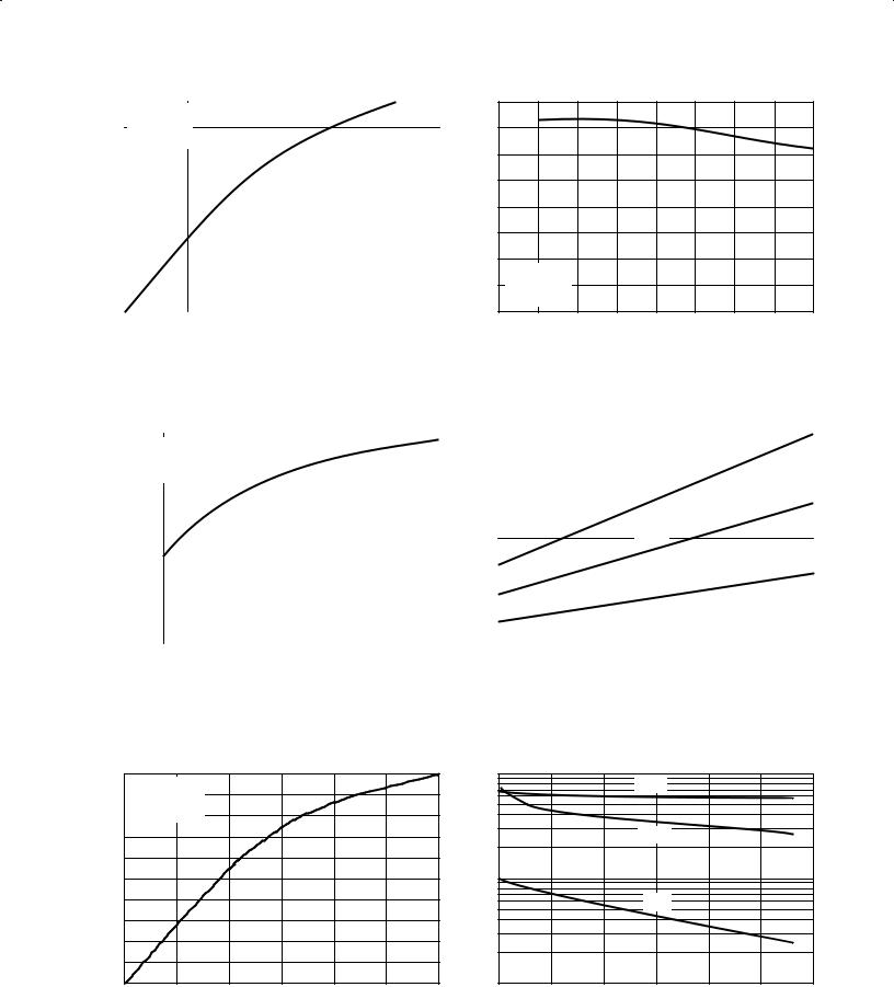
Figure 6. Output Power versus Input Power |
Figure 7. Capacitance versus Drain |
|
Source Voltage |
|
|
MRF182 |
MOTOROLA RF DEVICE DATA |
4 |
|

Table 1. Typical Common Source S±Parameters (VDS = 13.5 V)
ID = 1.0 A
f |
|
S11 |
|
S21 |
|
S12 |
|
S22 |
||||
MHz |
|S11| |
|
φ |
|S21| |
|
φ |
|S12| |
|
φ |
|S22| |
|
φ |
20 |
0.933 |
|
±131 |
40.81 |
|
112 |
0.021 |
|
22 |
0.664 |
|
±138 |
30 |
0.922 |
|
±148 |
29.31 |
|
104 |
0.022 |
|
15 |
0.700 |
|
±151 |
40 |
0.892 |
|
±156 |
22.19 |
|
99 |
0.022 |
|
10 |
0.718 |
|
±158 |
50 |
0.877 |
|
±161 |
17.91 |
|
95 |
0.023 |
|
7 |
0.725 |
|
±162 |
60 |
0.870 |
|
±164 |
14.67 |
|
92 |
0.023 |
|
4 |
0.732 |
|
±164 |
70 |
0.863 |
|
±166 |
12.57 |
|
90 |
0.022 |
|
2 |
0.735 |
|
±166 |
80 |
0.860 |
|
±168 |
11.00 |
|
89 |
0.022 |
|
1 |
0.738 |
|
±168 |
90 |
0.860 |
|
±169 |
9.79 |
|
87 |
0.022 |
|
0 |
0.740 |
|
±169 |
100 |
0.859 |
|
±170 |
8.79 |
|
86 |
0.022 |
|
±1 |
0.741 |
|
±169 |
150 |
0.859 |
|
±173 |
5.78 |
|
80 |
0.022 |
|
±7 |
0.750 |
|
±172 |
200 |
0.862 |
|
±175 |
4.29 |
|
74 |
0.022 |
|
±11 |
0.759 |
|
±172 |
250 |
0.868 |
|
±176 |
3.38 |
|
69 |
0.021 |
|
±14 |
0.770 |
|
±173 |
300 |
0.880 |
|
±177 |
2.77 |
|
65 |
0.020 |
|
±17 |
0.780 |
|
±173 |
350 |
0.877 |
|
±177 |
2.32 |
|
61 |
0.020 |
|
±19 |
0.793 |
|
±173 |
400 |
0.882 |
|
±178 |
1.98 |
|
56 |
0.019 |
|
±22 |
0.808 |
|
±173 |
450 |
0.892 |
|
±179 |
1.72 |
|
52 |
0.018 |
|
±24 |
0.816 |
|
±173 |
500 |
0.899 |
|
±180 |
1.51 |
|
49 |
0.017 |
|
±26 |
0.828 |
|
±174 |
550 |
0.898 |
|
180 |
1.33 |
|
45 |
0.017 |
|
±27 |
0.838 |
|
±174 |
600 |
0.907 |
|
179 |
1.19 |
|
42 |
0.016 |
|
±28 |
0.849 |
|
±175 |
650 |
0.914 |
|
179 |
1.07 |
|
38 |
0.015 |
|
±28 |
0.859 |
|
±175 |
700 |
0.916 |
|
177 |
0.95 |
|
35 |
0.014 |
|
±25 |
0.867 |
|
±176 |
750 |
0.920 |
|
177 |
0.88 |
|
34 |
0.015 |
|
±26 |
0.874 |
|
±176 |
800 |
0.924 |
|
176 |
0.80 |
|
30 |
0.015 |
|
±27 |
0.884 |
|
±177 |
850 |
0.929 |
|
175 |
0.74 |
|
27 |
0.015 |
|
±33 |
0.891 |
|
±178 |
900 |
0.929 |
|
174 |
0.68 |
|
25 |
0.013 |
|
±38 |
0.897 |
|
±178 |
950 |
0.933 |
|
173 |
0.63 |
|
22 |
0.011 |
|
±39 |
0.905 |
|
±179 |
1000 |
0.934 |
|
173 |
0.58 |
|
20 |
0.010 |
|
±37 |
0.912 |
|
±180 |
1050 |
0.930 |
|
172 |
0.54 |
|
17 |
0.009 |
|
±33 |
0.918 |
|
180 |
1100 |
0.938 |
|
171 |
0.52 |
|
15 |
0.009 |
|
±29 |
0.924 |
|
179 |
1150 |
0.933 |
|
170 |
0.48 |
|
13 |
0.008 |
|
±28 |
0.929 |
|
178 |
1200 |
0.930 |
|
169 |
0.45 |
|
10 |
0.008 |
|
±25 |
0.930 |
|
177 |
1250 |
0.939 |
|
168 |
0.42 |
|
8 |
0.007 |
|
±23 |
0.935 |
|
177 |
1300 |
0.936 |
|
168 |
0.40 |
|
6 |
0.007 |
|
±21 |
0.934 |
|
176 |
1350 |
0.933 |
|
167 |
0.38 |
|
4 |
0.006 |
|
±19 |
0.936 |
|
175 |
1400 |
0.937 |
|
166 |
0.35 |
|
2 |
0.005 |
|
±14 |
0.939 |
|
174 |
1450 |
0.937 |
|
165 |
0.33 |
|
0 |
0.005 |
|
±5 |
0.934 |
|
174 |
1500 |
0.927 |
|
164 |
0.32 |
|
±2 |
0.004 |
|
0 |
0.930 |
|
173 |
MOTOROLA RF DEVICE DATA |
MRF182 |
|
5 |

Table 2. Typical Common Emitter S±Parameters (VDS = 28 V)
ID = 1.0 A
f |
|
S11 |
|
S21 |
|
S12 |
|
S22 |
||||
MHz |
|S11| |
|
φ |
|S21| |
|
φ |
|S12| |
|
φ |
|S22| |
|
φ |
20 |
0.964 |
|
±99 |
54.39 |
|
129 |
0.014 |
|
39 |
0.429 |
|
±108 |
30 |
0.949 |
|
±121 |
43.46 |
|
118 |
0.017 |
|
28 |
0.478 |
|
±125 |
40 |
0.909 |
|
±134 |
34.35 |
|
109 |
0.018 |
|
20 |
0.520 |
|
±137 |
50 |
0.884 |
|
±142 |
28.27 |
|
103 |
0.018 |
|
15 |
0.540 |
|
±144 |
60 |
0.875 |
|
±148 |
23.38 |
|
98 |
0.019 |
|
11 |
0.553 |
|
±149 |
70 |
0.862 |
|
±152 |
20.10 |
|
95 |
0.019 |
|
8 |
0.562 |
|
±152 |
80 |
0.861 |
|
±156 |
17.64 |
|
92 |
0.019 |
|
5 |
0.569 |
|
±154 |
90 |
0.858 |
|
±158 |
15.72 |
|
90 |
0.019 |
|
3 |
0.575 |
|
±156 |
100 |
0.858 |
|
±160 |
14.11 |
|
88 |
0.019 |
|
1 |
0.580 |
|
±157 |
150 |
0.856 |
|
±166 |
9.26 |
|
79 |
0.018 |
|
±7 |
0.606 |
|
±160 |
200 |
0.862 |
|
±169 |
6.80 |
|
71 |
0.018 |
|
±12 |
0.633 |
|
±161 |
250 |
0.871 |
|
±171 |
5.29 |
|
65 |
0.017 |
|
±16 |
0.661 |
|
±161 |
300 |
0.882 |
|
±173 |
4.27 |
|
59 |
0.016 |
|
±21 |
0.690 |
|
±162 |
350 |
0.883 |
|
±174 |
3.52 |
|
54 |
0.015 |
|
±23 |
0.718 |
|
±162 |
400 |
0.895 |
|
±175 |
2.97 |
|
49 |
0.014 |
|
±26 |
0.747 |
|
±163 |
450 |
0.904 |
|
±176 |
2.54 |
|
45 |
0.013 |
|
±28 |
0.767 |
|
±164 |
500 |
0.911 |
|
±177 |
2.20 |
|
41 |
0.012 |
|
±30 |
0.789 |
|
±165 |
550 |
0.911 |
|
±178 |
1.90 |
|
37 |
0.011 |
|
±30 |
0.807 |
|
±166 |
600 |
0.923 |
|
±179 |
1.69 |
|
33 |
0.010 |
|
±30 |
0.825 |
|
±167 |
650 |
0.929 |
|
±180 |
1.50 |
|
30 |
0.009 |
|
±29 |
0.841 |
|
±168 |
700 |
0.929 |
|
179 |
1.32 |
|
26 |
0.009 |
|
±22 |
0.855 |
|
±169 |
750 |
0.933 |
|
178 |
1.21 |
|
24 |
0.010 |
|
±22 |
0.865 |
|
±170 |
800 |
0.938 |
|
177 |
1.09 |
|
21 |
0.009 |
|
±20 |
0.877 |
|
±171 |
850 |
0.942 |
|
176 |
1.00 |
|
18 |
0.010 |
|
±31 |
0.886 |
|
±172 |
900 |
0.942 |
|
175 |
0.92 |
|
16 |
0.008 |
|
±37 |
0.894 |
|
±173 |
950 |
0.947 |
|
174 |
0.84 |
|
13 |
0.006 |
|
±38 |
0.904 |
|
±174 |
1000 |
0.946 |
|
173 |
0.77 |
|
11 |
0.005 |
|
±28 |
0.912 |
|
±175 |
1050 |
0.943 |
|
172 |
0.72 |
|
8 |
0.005 |
|
±18 |
0.919 |
|
±176 |
1100 |
0.948 |
|
171 |
0.67 |
|
6 |
0.004 |
|
±9 |
0.926 |
|
±177 |
1150 |
0.945 |
|
171 |
0.62 |
|
4 |
0.005 |
|
0 |
0.932 |
|
±178 |
1200 |
0.939 |
|
170 |
0.59 |
|
1 |
0.004 |
|
3 |
0.934 |
|
±179 |
1250 |
0.949 |
|
169 |
0.54 |
|
0 |
0.005 |
|
12 |
0.940 |
|
±180 |
1300 |
0.947 |
|
168 |
0.51 |
|
±3 |
0.005 |
|
18 |
0.939 |
|
180 |
1350 |
0.944 |
|
167 |
0.48 |
|
±4 |
0.005 |
|
22 |
0.941 |
|
179 |
1400 |
0.945 |
|
166 |
0.44 |
|
±7 |
0.004 |
|
34 |
0.943 |
|
178 |
1450 |
0.944 |
|
165 |
0.42 |
|
±9 |
0.005 |
|
45 |
0.940 |
|
177 |
1500 |
0.933 |
|
164 |
0.40 |
|
±10 |
0.005 |
|
55 |
0.936 |
|
176 |
MRF182 |
MOTOROLA RF DEVICE DATA |
6 |
|

PACKAGE DIMENSIONS
|
|
G |
|
|
|
±B± |
|
1 |
|
|
|
|
|
|
|
|
|
|
|
|
3 |
|
|
|
|
2 |
Q 2 PL |
|
|
|
|
|
|
|
|
K |
|
D |
|
0.25 (0.010) M T A M B M |
|
|
|
|
|
||
|
|
|
|
|
|
H |
E |
N |
F |
C |
|
|
|
|
|||
|
|
|
|
±T± |
SEATING |
|
|
|
|
|
PLANE |
±A±
NOTES:
1.DIMENSIONING AND TOLERANCING PER ANSI Y14.5M, 1982.
2.CONTROLLING DIMENSION: INCH.
|
INCHES |
MILLIMETERS |
||
DIM |
MIN |
MAX |
MIN |
MAX |
A |
0.790 |
0.810 |
20.07 |
20.57 |
B |
0.220 |
0.240 |
5.59 |
6.09 |
C |
0.125 |
0.175 |
3.18 |
4.45 |
D |
0.205 |
0.225 |
5.21 |
5.71 |
E |
0.050 |
0.070 |
1.27 |
1.77 |
F |
0.004 |
0.006 |
0.11 |
0.15 |
G |
0.562 BSC |
14.27 BSC |
||
H |
0.070 |
0.090 |
1.78 |
2.29 |
K |
0.215 |
0.255 |
5.47 |
6.47 |
N |
0.350 |
0.370 |
8.89 |
9.39 |
Q |
0.120 |
0.140 |
3.05 |
3.55 |
STYLE 1: |
|
PIN 1. |
DRAIN |
2. |
GATE |
3. |
SOURCE |
CASE 360B±01
ISSUE O (MRF182)
|
1 |
|
|
±B± |
|
|
|
|
2 |
|
|
K |
D |
|
|
|
|
|
|
E |
N |
F |
|
|
|
||
H |
|
|
|
|
3 |
C |
±T± |
|
|
|
SEATING |
|
|
|
PLANE |
|
±A± |
|
|
NOTES:
1.DIMENSIONING AND TOLERANCING PER ANSI Y14.5M, 1982.
2.CONTROLLING DIMENSION: INCH.
|
INCHES |
MILLIMETERS |
||
DIM |
MIN |
MAX |
MIN |
MAX |
A |
0.370 |
0.390 |
9.40 |
9.91 |
B |
0.220 |
0.240 |
5.59 |
6.09 |
C |
0.105 |
0.155 |
2.67 |
3.94 |
D |
0.205 |
0.225 |
5.21 |
5.71 |
E |
0.035 |
0.045 |
0.89 |
1.14 |
F |
0.004 |
0.006 |
0.11 |
0.15 |
H |
0.057 |
0.067 |
1.45 |
1.70 |
K |
0.085 |
0.115 |
2.16 |
2.92 |
N |
0.350 |
0.370 |
8.89 |
9.39 |
STYLE 1:
PIN 1. DRAIN
2.GATE
3.SOURCE
CASE 360C±03
ISSUE B (MRF182S)
MOTOROLA RF DEVICE DATA |
MRF182 |
|
7 |

Motorola reserves the right to make changes without further notice to any products herein. Motorola makes no warranty, representation or guarantee regarding the suitability of its products for any particular purpose, nor does Motorola assume any liability arising out of the application or use of any product or circuit, and specifically disclaims any and all liability, including without limitation consequential or incidental damages. ªTypicalº parameters which may be provided in Motorola data sheets and/or specifications can and do vary in different applications and actual performance may vary over time. All operating parameters, including ªTypicalsº must be validated for each customer application by customer's technical experts. Motorola does not convey any license under its patent rights nor the rights of others. Motorola products are not designed, intended, or authorized for use as components in systems intended for surgical implant into the body, or other applications intended to support or sustain life, or for any other application in which the failure of the Motorola product could create a situation where personal injury or death may occur. Should Buyer purchase or use Motorola products for any such unintended or unauthorized application, Buyer shall indemnify and hold Motorola and its officers, employees, subsidiaries, affiliates, and distributors harmless against all claims, costs, damages, and expenses, and reasonable attorney fees arising out of, directly or indirectly, any claim of personal injury or death associated with such unintended or unauthorized use, even if such claim alleges that Motorola was negligent regarding the design or manufacture of the part. Motorola and  are registered trademarks of Motorola, Inc. Motorola, Inc. is an Equal Opportunity/Affirmative Action Employer.
|
Mfax is a trademark of Motorola, Inc. |
How to reach us: |
|
USA / EUROPE / Locations Not Listed: Motorola Literature Distribution; |
JAPAN: Nippon Motorola Ltd.: SPD, Strategic Planning Office, 4±32±1, |
P.O. Box 5405, Denver, Colorado 80217. 303±675±2140 or 1±800±441±2447 |
Nishi±Gotanda, Shinagawa±ku, Tokyo 141, Japan. 81±3±5487±8488 |
Mfax : RMFAX0@email.sps.mot.com ± TOUCHTONE 602±244±6609 |
ASIA/PACIFIC: Motorola Semiconductors H.K. Ltd.; 8B Tai Ping Industrial Park, |
± US & Canada ONLY 1±800±774±1848 51 Ting Kok Road, Tai Po, N.T., Hong Kong. 852±26629298
INTERNET: http://motorola.com/sps
MRF182 |
◊ |
MRF182/D |
|
MOTOROLA RF DEVICE DATA |
|
8 |
|
|