

MOTOROLA
SEMICONDUCTOR TECHNICAL DATA
Order this document by MRF151G/D
The RF MOSFET Line |
|
|
|
|
|
|
|
|
|
|
|
|
|
|
|
|||||||
RF Power Field-Effect Transistor |
|
|
|
|
|
|
|
|
|
|
|
|||||||||||
N±Channel Enhancement±Mode MOSFET |
|
|
|
|
|
MRF151G |
|
|
|
|
||||||||||||
Designed for broadband commercial and military applications at frequencies |
|
|
|
|
|
|
|
|
|
|
|
|||||||||||
to 175 MHz. The high power, high gain and broadband performance of this |
|
|
|
|
|
|
|
|
|
|
|
|||||||||||
device makes possible solid state transmitters for FM broadcast or TV channel |
|
|
|
|
|
|
|
|
|
|
|
|||||||||||
|
|
|
|
|
|
|
|
|
|
|
||||||||||||
frequency bands. |
|
|
|
|
|
|
|
|
|
|
|
|
|
|
|
|||||||
|
|
|
|
|
|
|
|
|
|
|
|
|
|
|
||||||||
• Guaranteed Performance at 175 MHz, 50 V: |
|
|
|
|
|
300 W, 50 V, 175 MHz |
|
|
|
|
||||||||||||
Output Power Ð 300 W |
|
|
|
|
|
|
N±CHANNEL |
|
|
|
|
|||||||||||
Gain Ð 14 dB (16 dB Typ) |
|
|
|
|
|
|
BROADBAND |
|
|
|
|
|||||||||||
Efficiency Ð 50% |
|
|
|
|
|
|
RF POWER MOSFET |
|
|
|
|
|||||||||||
• Low Thermal Resistance Ð 0.35 °C/W |
|
|
|
|
|
|
|
|
|
|
|
|
|
|
|
|||||||
|
|
|
|
|
|
|
|
|
|
|
|
|
|
|
||||||||
• Ruggedness Tested at Rated Output Power |
|
|
|
|
|
|
|
|
|
|
|
|
|
|
|
|||||||
|
|
|
|
|
|
|
|
|
|
|
|
|
|
|
||||||||
• Nitride Passivated Die for Enhanced Reliability |
|
|
|
|
|
|
|
|
|
|
|
|
|
|
|
|||||||
G |
|
|
|
D |
|
|
|
|
|
S |
|
|
|
|
|
|
|
|
|
|
|
|
|
|
|
|
|
|
|
|
|
|
|
|
|
|
|
|
|
|
|
|
|||
|
|
|
|
|
|
|
|
|
|
|
|
|
|
|
|
|
|
|
|
|||
|
|
|
|
|
|
|
|
|
|
|
|
|
|
|
|
|
|
|
|
|||
|
|
|
|
|
|
|
|
|
|
|
|
|
|
|||||||||
|
|
|
|
|
|
|
|
|
|
|
|
|
|
|
|
|
|
|||||
|
|
|
|
|
|
|
|
|
|
|
|
|
|
|
|
|
|
|
|
|
||
|
|
|
|
|
|
|
|
|
|
|
|
|
|
|
|
|
|
|
|
|
|
|
|
|
|
|
|
|
|
|
|
|
|
|
|
|
|
|
|
|
|
|
|
|
|
G |
|
|
|
|
|
|
(FLANGE) |
|
CASE 375±04, STYLE 2 |
|
|
|
|
|||||||||
|
|
|
|
|
|
|
|
|
|
|
|
|
||||||||||
|
|
|
|
|
|
|
|
|
|
|
|
|
||||||||||
|
|
|
|
|
|
|
|
|
|
|
|
|
|
|
|
|
||||||
|
|
|
|
|
|
|
|
|
|
|
|
|
|
|
|
|
||||||
|
|
|
|
D |
|
|
|
|
|
|
|
|
|
|
|
|
|
|
|
|
|
|
|
|
|
|
|
|
|
|
|
|
|
|
|
|
|
|
|||||||
MAXIMUM RATINGS |
|
|
|
|
|
|
|
|
|
|
|
|
|
|
|
|||||||
|
|
|
|
|
|
|
|
|
|
|
|
|
|
|
||||||||
|
|
|
|
|
|
|
|
|
|
|
|
|
|
|
|
|
|
|
|
|
|
|
Rating |
|
|
Symbol |
|
|
Value |
|
|
|
Unit |
||||||||||||
|
|
|
|
|
|
|
|
|
|
|
|
|
|
|
|
|
|
|
|
|
|
|
Drain±Source Voltage |
|
|
VDSS |
|
125 |
|
|
|
|
|
Vdc |
|||||||||||
Drain±Gate Voltage |
|
|
VDGO |
|
125 |
|
|
|
|
|
Vdc |
|||||||||||
Gate±Source Voltage |
|
|
VGS |
|
± 40 |
|
|
|
|
|
Vdc |
|||||||||||
Drain Current Ð Continuous |
|
|
ID |
|
40 |
|
|
|
|
|
Adc |
|||||||||||
Total Device Dissipation @ TC = 25°C |
|
|
PD |
|
500 |
|
|
|
|
|
Watts |
|||||||||||
Derate above 25°C |
|
|
|
|
|
2.85 |
|
|
|
|
|
W/°C |
||||||||||
|
|
|
|
|
|
|
|
|
|
|
|
|
|
|
|
|
|
|
|
|
|
|
Storage Temperature Range |
|
|
Tstg |
|
|
± 65 to +150 |
|
|
|
°C |
||||||||||||
Operating Junction Temperature |
|
|
TJ |
|
200 |
|
|
|
|
|
°C |
|||||||||||
THERMAL CHARACTERISTICS |
|
|
|
|
|
|
|
|
|
|
|
|
|
|
|
|||||||
|
|
|
|
|
|
|
|
|
|
|
|
|
|
|
|
|
|
|
|
|
||
Characteristic |
|
|
Symbol |
|
|
Max |
|
|
|
Unit |
||||||||||||
|
|
|
|
|
|
|
|
|
|
|
|
|
|
|
|
|
|
|
|
|
|
|
Thermal Resistance, Junction to Case |
|
|
RθJC |
|
0.35 |
|
|
|
|
|
°C/W |
|||||||||||
NOTE Ð CAUTION Ð MOS devices are susceptible to damage from electrostatic charge. Reasonable precautions in handling and packaging MOS devices should be observed.
REV 8
MOTOROLAMotorola, Inc. 1997RF DEVICE DATA |
MRF151G |
|
1 |
ELECTRICAL CHARACTERISTICS (TC = 25°C unless otherwise noted.)
Characteristic |
Symbol |
Min |
Typ |
Max |
Unit |
|
|
|
|
|
|
OFF CHARACTERISTICS (Each Side)
Drain±Source Breakdown Voltage (VGS = 0, ID = 100 mA) |
V(BR)DSS |
125 |
|
Ð |
Ð |
|
Vdc |
Zero Gate Voltage Drain Current (VDS = 50 V, VGS = 0) |
IDSS |
Ð |
|
Ð |
5.0 |
|
mAdc |
Gate±Body Leakage Current (VGS = 20 V, VDS = 0) |
IGSS |
Ð |
|
Ð |
1.0 |
|
mAdc |
ON CHARACTERISTICS (Each Side) |
|
|
|
|
|
|
|
|
|
|
|
|
|
|
|
Gate Threshold Voltage (VDS = 10 V, ID = 100 mA) |
VGS(th) |
1.0 |
|
3.0 |
5.0 |
|
Vdc |
Drain±Source On±Voltage (VGS = 10 V, ID = 10 A) |
VDS(on) |
1.0 |
|
3.0 |
5.0 |
|
Vdc |
Forward Transconductance (VDS = 10 V, ID = 5.0 A) |
gfs |
5.0 |
|
7.0 |
Ð |
|
mhos |
DYNAMIC CHARACTERISTICS (Each Side) |
|
|
|
|
|
|
|
|
|
|
|
|
|
|
|
Input Capacitance (VDS = 50 V, VGS = 0, f = 1.0 MHz) |
Ciss |
Ð |
|
350 |
Ð |
|
pF |
Output Capacitance (VDS = 50 V, VGS = 0, f = 1.0 MHz) |
Coss |
Ð |
|
220 |
Ð |
|
pF |
Reverse Transfer Capacitance (VDS = 50 V, VGS = 0, f = 1.0 MHz) |
Crss |
Ð |
|
15 |
Ð |
|
pF |
FUNCTIONAL TESTS |
|
|
|
|
|
|
|
|
|
|
|
|
|
|
|
Common Source Amplifier Power Gain |
Gps |
14 |
|
16 |
Ð |
|
dB |
(VDD = 50 V, Pout = 300 W, IDQ = 500 mA, f = 175 MHz) |
|
|
|
|
|
|
|
Drain Efficiency |
h |
50 |
|
55 |
Ð |
|
% |
(VDD = 50 V, Pout = 300 W, f = 175 MHz, ID (Max) = 11 A) |
|
|
|
|
|
|
|
Load Mismatch |
y |
|
|
|
|
|
|
(VDD = 50 V, Pout = 300 W, IDQ = 500 mA, |
|
|
No Degradation in Output Power |
|
|||
VSWR 5:1 at all Phase Angles) |
|
|
|
|
|
|
|
|
|
|
|
|
|
|
|
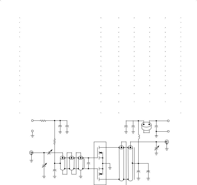
R1 |
|
|
|
L2 |
|
+ |
|
|
|
+ |
|
|
|
|
|
||
C4 |
C5 |
C9 |
C10 |
|
50 V |
BIAS 0 ± 6 V |
|
|
|
C11 |
|
± |
|
|
|
|
± |
|
|
|
L1 |
|
|
R2 |
D.U.T. |
T2 |
|
|
OUTPUT |
|
|
|
|
||
C1 |
T1 |
|
|
C12 |
|
|
|
|
|
||
INPUT |
|
|
|
|
|
|
|
|
|
|
|
|
C6 |
|
|
|
|
C2 |
|
|
|
|
|
C3 |
|
|
C7 |
C8 |
|
|
|
|
|
R1 |
Ð 100 Ohms, 1/2 W |
|
|
|
|
|
|
|
|
|
|
|
R2 |
Ð 1.0 kOhm, 1/2 W |
|
|
|
|
|
|
|
|
|
|
|
|
|
|
|
|
|
|
|
|
|
|||
C1 |
Ð Arco 424 |
|
|
|
|
|
|
|
|
|
|
|
|
|
|
|
|
|
|
|
|
|
|||
|
|
|
|
|
|
|
|
|
|
|||
C2 |
Ð Arco 404 |
T1 Ð 9:1 RF Transformer. Can be made of 15 ± 18 Ohms |
||||||||||
C3, C4, C7, C8, C9 Ð 1000 pF Chip |
||||||||||||
Semirigid Co±Ax, 62 ± 90 Mils O.D. |
||||||||||||
C5, C10 Ð 0.1 mF Chip |
||||||||||||
C6 |
Ð 330 pF Chip |
T2 Ð 1:4 RF Transformer. Can be made of 16 ± 18 Ohms |
||||||||||
Semirigid Co±Ax, 70±90 Mils O.D. |
||||||||||||
C11 Ð 0.47 mF Ceramic Chip, Kemet 1215 or |
||||||||||||
|
Equivalent (100 V) |
Board Material Ð 0.062 ″ Fiberglass (G10), |
||||||||||
C12 Ð Arco 422 |
1 oz. Copper Clad, 2 Sides, er = 5.0 |
|||||||||||
L1 Ð 10 Turns AWG #18 Enameled Wire, |
NOTE: For stability, the input transformer T1 must be loaded |
|||||||||||
|
Close Wound, 1/4″ I.D. |
with ferrite toroids or beads to increase the common |
||||||||||
L2 Ð Ferrite Beads of Suitable Material for |
mode inductance. For operation below 100 MHz. The |
|||||||||||
|
1.5± 2.0 mH Total Inductance |
same is required for the output transformer. |
||||||||||
Unless Otherwise Noted, All Chip Capacitors are ATC Type 100 or |
See Figure 6 for construction details of T1 and T2. |
|||||||||||
Equivalent. |
|
|
|
|
|
|
|
|
|
|
||
|
Figure 1. 175 MHz Test Circuit |
|||||||||||
|
|
|
|
|
|
|
|
|
|
|
||
MRF151G |
|
|
|
|
|
|
|
|
|
MOTOROLA RF DEVICE DATA |
||
2 |
|
|
|
|
|
|
|
|
|
|
|
|
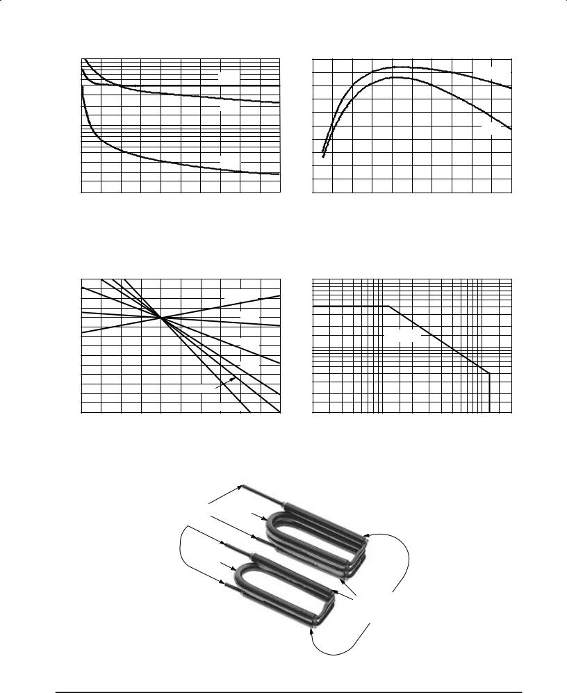
C, CAPACITANCE (pF)
|
|
|
|
|
TYPICAL CHARACTERISTICS |
|
|
|
|
|
|
|
|
||||
1000 |
|
|
|
|
|
|
2000 |
|
|
|
|
|
|
|
|
|
|
500 |
|
|
|
|
Ciss |
(MHz) |
|
|
|
|
|
|
|
|
|
VDS = 30 V |
|
|
|
|
|
|
|
|
|
|
|
|
|
|
|
|
|||
|
|
|
|
FREQUENCY |
|
|
|
|
|
|
|
|
|
|
|
||
100 |
|
|
|
|
Coss |
1000 |
|
|
|
|
|
|
|
|
15 V |
|
|
200 |
|
|
|
|
|
|
|
|
|
|
|
|
|
|
|
|
|
50 |
|
|
|
|
|
GAIN |
|
|
|
|
|
|
|
|
|
|
|
|
|
|
|
|
UNITY |
|
|
|
|
|
|
|
|
|
|
|
|
|
|
|
|
|
Crss |
|
|
|
|
|
|
|
|
|
|
|
|
|
|
|
|
|
|
, |
|
|
|
|
|
|
|
|
|
|
|
20 |
|
|
|
|
|
T |
|
|
|
|
|
|
|
|
|
|
|
|
|
|
|
|
f |
|
|
|
|
|
|
|
|
|
|
|
|
0 |
0 |
10 |
20 |
30 |
40 |
50 |
0 0 |
2 |
4 |
6 |
8 |
10 |
12 |
14 |
16 |
18 |
20 |
VDS, DRAIN±SOURCE VOLTAGE (VOLTS) ID, DRAIN CURRENT (AMPS)
Figure 2. Capacitance versus |
Figure 3. Common Source Unity Gain Frequency |
Drain±Source Voltage* |
versus Drain Current* |
*Data shown applies to each half of MRF151G. |
|
(NORMALIZED) |
1.04 |
|
|
|
|
|
1.03 |
|
|
|
ID = 5 A |
|
|
1.02 |
|
|
|
|
||
1.01 |
|
|
|
|
|
|
1 |
|
|
|
4 A |
|
|
VOLTAGE |
|
|
|
|
||
0.99 |
|
|
|
|
|
|
0.98 |
|
|
|
2 A |
|
|
0.97 |
|
|
|
|
||
-SOURCE |
0.96 |
|
|
|
|
|
0.95 |
|
|
|
1 A |
|
|
0.94 |
|
|
|
|
||
|
|
|
|
|
||
DRAIN |
0.93 |
|
|
250 mA |
|
|
0.92 |
|
|
|
|
||
, |
0.91 |
|
|
|
|
|
GS |
|
|
|
100 mA |
|
|
0.9 |
|
|
|
|
||
V |
0 |
25 |
50 |
75 |
100 |
|
|
± 25 |
|||||
|
|
|
TC, CASE TEMPERATURE (°C) |
|
||
|
100 |
|
|
(AMPS) |
|
|
|
, DRAIN CURRENT |
|
TC = 25°C |
|
10 |
|
|
|
|
|
|
|
D |
|
|
|
I |
|
|
|
|
1 2 |
20 |
200 |
VDS, DRAIN±TO±SOURCE VOLTAGE (VOLTS)
Figure 4. Gate±Source Voltage versus |
Figure 5. DC Safe Operating Area |
||
Case Temperature* |
|
|
|
|
|
9:1 |
|
HIGH IMPEDANCE |
CENTER |
IMPEDANCE |
|
TAP |
RATIO |
||
WINDINGS |
|||
|
|
||
CENTER |
|
|
|
TAP |
|
|
|
|
|
CONNECTIONS |
|
|
|
TO LOW IMPEDANCE |
|
|
4:1 |
WINDINGS |
|
|
IMPEDANCE |
|
|
|
RATIO |
|
|
|
Figure 6. RF Transformer |
||
MOTOROLA RF DEVICE DATA |
|
MRF151G |
|
|
|
3 |
|
Pout, OUTPUT POWER (WATTS)
|
|
|
TYPICAL CHARACTERISTICS |
|
|
|
|
||||
350 |
|
|
175 MHz |
|
30 |
|
|
|
|
|
|
|
|
f = 150 MHz |
|
|
|
|
|
|
|
|
|
|
|
|
|
|
|
|
|
|
|
|
|
300 |
|
|
200 MHz |
|
25 |
|
|
|
|
|
|
|
|
|
(dB) |
|
|
|
|
|
|
||
250 |
|
|
|
|
|
|
|
|
|
|
|
200 |
|
|
|
GAIN |
20 |
|
|
|
|
|
|
|
|
|
|
|
|
|
|
|
|
||
|
|
|
POWER, |
|
|
|
|
|
|
|
|
150 |
|
|
|
15 |
|
VDD = 50 V |
|
|
|
|
|
|
|
|
|
|
|
|
|
|
|
|
|
100 |
|
|
VDD = 50 V |
PS |
|
|
I = 2 x 250 mA |
|
|
|
|
|
|
G |
|
|
DQ |
|
|
|
|
||
50 |
|
|
IDQ = 2 x 250 mA |
|
10 |
|
Pout = 150 W |
|
|
|
|
|
|
|
|
|
|
|
|
|
|
|
|
0 |
0 |
|
5 |
10 |
5 |
2 |
5 |
10 |
30 |
100 |
200 |
|
|
Pin, INPUT POWER (WATTS) |
|
|
|
|
f, FREQUENCY (MHz) |
|
|
||
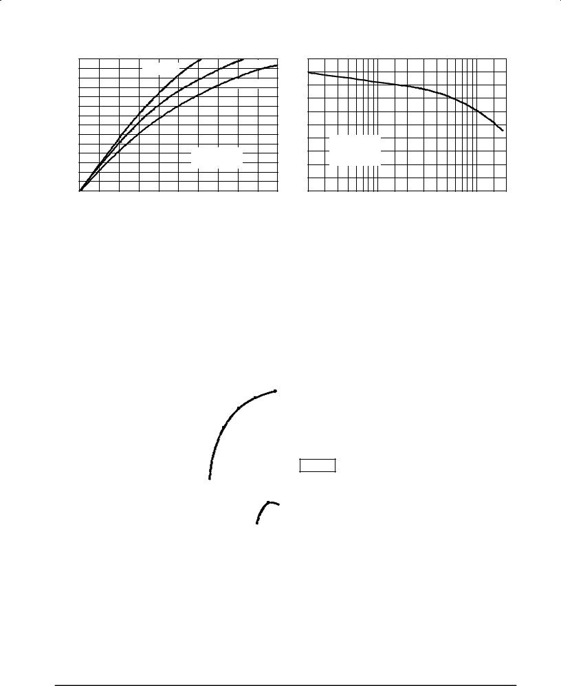
Figure 7. Output Power versus Input Power |
Figure 8. Power Gain versus Frequency |
f = 175 MHz
|
150 |
|
|
125 |
|
100 |
INPUT, Zin |
|
(GATE TO GATE) |
||
|
Zo = 10 Ω
30 
125 150
100 
 f = 175 MHz
30  OUTPUT, ZOL* (DRAIN TO DRAIN)
ZOL* = Conjugate of the optimum load impedance
ZOL* = into which the device output operates at a
ZOL* = given output power, voltage and frequency.
Figure 9. Input and Output Impedance
MRF151G |
MOTOROLA RF DEVICE DATA |
4 |
|
RF POWER MOSFET CONSIDERATIONS
MOSFET CAPACITANCES
The physical structure of a MOSFET results in capacitors between the terminals. The metal anode gate structure determines the capacitors from gate±to±drain (Cgd), and gate± to±source (Cgs). The PN junction formed during the fabrication of the RF MOSFET results in a junction capacitance from drain±to±source (Cds).
These capacitances are characterized as input (Ciss), output (Coss) and reverse transfer (Crss) capacitances on data sheets. The relationships between the inter±terminal capacitances and those given on data sheets are shown below. The Ciss can be specified in two ways:
1.Drain shorted to source and positive voltage at the gate.
2.Positive voltage of the drain in respect to source and zero volts at the gate. In the latter case the numbers are lower. However, neither method represents the actual operating conditions in RF applications.
DRAIN |
|
|
|
|
|
Cgd |
|
|
|
|
|
GATE |
Ciss = Cgd = Cgs |
||||
Cds |
C |
= C |
gd |
= C |
ds |
|
oss |
|
|
||
|
Crss = Cgd |
|
|
||
Cgs |
|
|
|
|
|
SOURCE |
|
|
|
|
|
LINEARITY AND GAIN CHARACTERISTICS
In addition to the typical IMD and power gain data presented, Figure 3 may give the designer additional information on the capabilities of this device. The graph represents the small signal unity current gain frequency at a given drain current level. This is equivalent to fT for bipolar transistors. Since this test is performed at a fast sweep speed, heating of the device does not occur. Thus, in normal use, the higher temperatures may degrade these characteristics to some extent.
DRAIN CHARACTERISTICS
One figure of merit for a FET is its static resistance in the full±on condition. This on±resistance, VDS(on), occurs in the linear region of the output characteristic and is specified under specific test conditions for gate±source voltage and drain current. For MOSFETs, VDS(on) has a positive temperature coefficient and constitutes an important design consideration at high temperatures, because it contributes to the power dissipation within the device.
GATE CHARACTERISTICS
The gate of the MOSFET is a polysilicon material, and is electrically isolated from the source by a layer of oxide. The input resistance is very high Ð on the order of 10 9 ohms Ð resulting in a leakage current of a few nanoamperes.
Gate control is achieved by applying a positive voltage slightly in excess of the gate±to±source threshold voltage,
VGS(th).
Gate Voltage Rating Ð Never exceed the gate voltage rating. Exceeding the rated VGS can result in permanent damage to the oxide layer in the gate region.
Gate Termination Ð The gates of these devices are essentially capacitors. Circuits that leave the gate open±cir-
cuited or floating should be avoided. These conditions can result in turn±on of the devices due to voltage build±up on the input capacitor due to leakage currents or pickup.
Gate Protection Ð These devices do not have an internal monolithic zener diode from gate±to±source. If gate protection is required, an external zener diode is recommended.
Using a resistor to keep the gate±to±source impedance low also helps damp transients and serves another important function. Voltage transients on the drain can be coupled to the gate through the parasitic gate±drain capacitance. If the gate±to±source impedance and the rate of voltage change on the drain are both high, then the signal coupled to the gate may be large enough to exceed the gate±threshold voltage and turn the device on.
HANDLING CONSIDERATIONS
When shipping, the devices should be transported only in antistatic bags or conductive foam. Upon removal from the packaging, careful handling procedures should be adhered to. Those handling the devices should wear grounding straps and devices not in the antistatic packaging should be kept in metal tote bins. MOSFETs should be handled by the case and not by the leads, and when testing the device, all leads should make good electrical contact before voltage is applied. As a final note, when placing the FET into the system it is designed for, soldering should be done with a grounded iron.
DESIGN CONSIDERATIONS
The MRF151G is an RF Power, MOS, N±channel enhancement mode field±effect transistor (FET) designed for HF and VHF power amplifier applications.
Motorola Application Note AN211A, FETs in Theory and Practice, is suggested reading for those not familiar with the construction and characteristics of FETs.
The major advantages of RF power MOSFETs include high gain, low noise, simple bias systems, relative immunity from thermal runaway, and the ability to withstand severely mismatched loads without suffering damage. Power output can be varied over a wide range with a low power dc control signal.
DC BIAS
The MRF151G is an enhancement mode FET and, therefore, does not conduct when drain voltage is applied. Drain current flows when a positive voltage is applied to the gate. RF power FETs require forward bias for optimum performance. The value of quiescent drain current (IDQ) is not critical for many applications. The MRF151G was characterized at IDQ = 250 mA, each side, which is the suggested minimum value of IDQ. For special applications such as linear amplification, IDQ may have to be selected to optimize the critical parameters.
The gate is a dc open circuit and draws no current. Therefore, the gate bias circuit may be just a simple resistive divider network. Some applications may require a more elaborate bias sytem.
GAIN CONTROL
Power output of the MRF151G may be controlled from its rated value down to zero (negative gain) by varying the dc gate voltage. This feature facilitates the design of manual gain control, AGC/ALC and modulation systems.
MOTOROLA RF DEVICE DATA |
MRF151G |
|
5 |
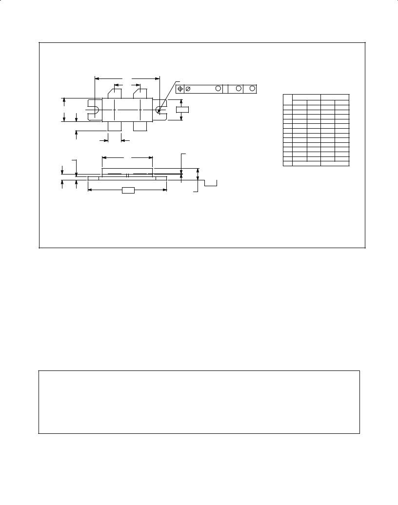
PACKAGE DIMENSIONS
|
|
U |
Q RADIUS 2 PL |
|
|
|
|
|
|
NOTES: |
|
|
|
|
|
|
|
|
|
|
|
|
1. DIMENSIONING AND TOLERANCING PER ANSI |
||||||
|
|
G |
|
|
|
|
|
|
||||||
|
|
0.25 (0.010) M |
T |
A |
M |
B |
M |
Y14.5M, 1982. |
|
|
|
|||
|
|
|
2. CONTROLLING DIMENSION: INCH. |
|
||||||||||
|
1 |
|
2 |
|
|
|
|
|
|
|
INCHES |
MILLIMETERS |
||
|
|
|
|
|
|
|
|
|
|
|
||||
|
|
|
|
|
|
|
|
|
|
DIM |
MIN |
MAX |
MIN |
MAX |
R |
|
|
±B± |
|
|
|
|
|
|
A |
1.330 |
1.350 |
33.79 |
34.29 |
|
|
|
|
|
|
|
|
B |
0.370 |
0.410 |
9.40 |
10.41 |
||
|
|
|
|
|
|
|
|
|
|
|||||
|
|
|
5 |
|
|
|
|
|
|
C |
0.190 |
0.230 |
4.83 |
5.84 |
K |
3 |
|
4 |
|
|
|
|
|
|
D |
0.215 |
0.235 |
5.47 |
5.96 |
|
|
|
|
|
|
|
E |
0.050 |
0.070 |
1.27 |
1.77 |
|||
|
|
|
|
|
|
|
|
|
|
G |
0.430 |
0.440 |
10.92 |
11.18 |
|
D |
|
|
|
|
|
|
|
|
H |
0.102 |
0.112 |
2.59 |
2.84 |
|
|
|
|
|
|
|
|
|
J |
0.004 |
0.006 |
0.11 |
0.15 |
|
|
|
|
|
|
|
|
|
|
|
K |
0.185 |
0.215 |
4.83 |
5.33 |
|
|
|
J |
|
|
|
|
|
|
N |
0.845 |
0.875 |
21.46 |
22.23 |
E |
|
N |
|
|
|
|
|
|
Q |
0.060 |
0.070 |
1.52 |
1.78 |
|
|
|
|
|
|
|
|
|
R |
0.390 |
0.410 |
9.91 |
10.41 |
||
|
|
|
|
|
|
|
|
|
||||||
|
|
|
|
|
|
|
|
|
|
U |
1.100 BSC |
27.94 BSC |
||
H |
|
|
|
SEATING |
|
|
|
|
|
STYLE 2: |
|
|||
|
|
|
±T± |
|
|
|
|
|
PIN |
1. DRAIN |
|
|||
|
|
±A± |
|
PLANE |
|
|
|
|
|
|
|
2. DRAIN |
|
|
|
|
C |
|
|
|
|
|
|
|
|
|
3. GATE |
|
|
|
|
|
|
|
|
|
|
|
|
|
|
4. GATE |
|
|
|
|
|
|
|
|
|
|
|
|
|
|
|
|
|
|
|
|
|
|
|
|
|
|
|
|
|
|
5. SOURCE |
|
CASE 375±04
ISSUE D
Motorola reserves the right to make changes without further notice to any products herein. Motorola makes no warranty, representation or guarantee regarding the suitability of its products for any particular purpose, nor does Motorola assume any liability arising out of the application or use of any product or circuit, and specifically disclaims any and all liability, including without limitation consequential or incidental damages. ªTypicalº parameters can and do vary in different applications. All operating parameters, including ªTypicalsº must be validated for each customer application by customer's technical experts. Motorola does not convey any license under its patent rights nor the rights of others. Motorola products are not designed, intended, or authorized for use as components in systems intended for surgical implant into the body, or other applications intended to support or sustain life, or for any other application in which the failure of the Motorola product could create a situation where personal injury or death may occur. Should Buyer purchase or use Motorola products for any such unintended or unauthorized application, Buyer shall indemnify and hold Motorola and its officers, employees, subsidiaries, affiliates, and distributors harmless against all claims, costs, damages, and expenses, and reasonable attorney fees arising out of, directly or indirectly, any claim of personal injury or death associated with such unintended or unauthorized use, even if such claim alleges that Motorola was negligent regarding the design or manufacture of the part. Motorola and  are registered trademarks of Motorola, Inc. Motorola, Inc. is an Equal Opportunity/Affirmative Action Employer.
How to reach us: |
|
USA / EUROPE: Motorola Literature Distribution; |
JAPAN: Nippon Motorola Ltd.; Tatsumi±SPD±JLDC, Toshikatsu Otsuki, |
P.O. Box 20912; Phoenix, Arizona 85036. 1±800±441±2447 |
6F Seibu±Butsuryu±Center, 3±14±2 Tatsumi Koto±Ku, Tokyo 135, Japan. 03±3521±8315 |
MFAX: RMFAX0@email.sps.mot.com ± TOUCHTONE (602) 244±6609 HONG KONG: Motorola Semiconductors H.K. Ltd.; 8B Tai Ping Industrial Park, |
|
INTERNET: http://Design±NET.com |
51 Ting Kok Road, Tai Po, N.T., Hong Kong. 852±26629298 |
◊ |
MRF151G/D |
|
MOTOROLA RF DEVICE DATA |
|
*MRF151G/D* |