

MOTOROLA
SEMICONDUCTOR TECHNICAL DATA
Order this document by MRF157/D
The RF Power MOS Line |
|
Power Field Effect |
Transistor |
N±Channel Enhancement Mode |
MRF157 |
Designed primarily for linear large±signal output stages to 80 MHz.
• Specified 50 Volts, 30 MHz Characteristics Output Power = 600 Watts
Power Gain = 21 dB (Typ)
Efficiency = 45% (Typ)
600 W, to 80 MHz MOS LINEAR RF POWER FET
D
G
S
CASE 368±03, STYLE 2
MAXIMUM RATINGS
Rating |
Symbol |
Value |
Unit |
|
|
|
|
Drain±Source Voltage |
VDSS |
125 |
Vdc |
Drain±Gate Voltage |
VDGO |
125 |
Vdc |
Gate±Source Voltage |
VGS |
± 40 |
Vdc |
Drain Current Ð Continuous |
ID |
60 |
Adc |
Total Device Dissipation @ TC = 25°C |
PD |
1350 |
Watts |
Derate above 25°C |
|
7.7 |
W/°C |
|
|
|
|
Storage Temperature Range |
Tstg |
± 65 to +150 |
°C |
Operating Junction Temperature |
TJ |
200 |
°C |
THERMAL CHARACTERISTICS |
|
|
|
|
|
|
|
Characteristic |
Symbol |
Max |
Unit |
|
|
|
|
Thermal Resistance, Junction to Case |
RθJC |
0.13 |
°C/W |
NOTE Ð CAUTION Ð MOS devices are susceptible to damage from electrostatic charge. Reasonable precautions in handling and packaging MOS devices should be observed.
REV 1
Motorola, Inc. 1995
ELECTRICAL CHARACTERISTICS (TC = 25°C unless otherwise noted)
Characteristic |
Symbol |
Min |
Typ |
Max |
Unit |
|
|
|
|
|
|
OFF CHARACTERISTICS
Drain±Source Breakdown Voltage (VGS = 0, ID = 100 mA) |
V(BR)DSS |
125 |
Ð |
Ð |
Vdc |
Zero Gate Voltage Drain Current (VDS = 50 V, VGS = 0) |
IDSS |
Ð |
Ð |
20 |
mAdc |
Gate±Body Leakage Current (VGS = 20 V, VDS = 0) |
IGSS |
Ð |
Ð |
5.0 |
mAdc |
ON CHARACTERISTICS |
|
|
|
|
|
|
|
|
|
|
|
Gate Threshold Voltage (VDS = 10 V, ID = 100 mA) |
VGS(th) |
1.0 |
3.0 |
5.0 |
Vdc |
Drain±Source On±Voltage (VGS = 10 V, ID = 40 A) |
VDS(on) |
1.0 |
3.0 |
5.0 |
Vdc |
Forward Transconductance (VDS = 10 V, ID = 20 A) |
gfs |
16 |
24 |
Ð |
mhos |
DYNAMIC CHARACTERISTICS |
|
|
|
|
|
|
|
|
|
|
|
Input Capacitance |
Ciss |
Ð |
1800 |
Ð |
pF |
(VDS = 50 V, VGS = 0 V, f = 1.0 MHz) |
|
|
|
|
|
Output Capacitance |
Coss |
Ð |
750 |
Ð |
pF |
(VDS = 50 V, VGS = 0, f = 1.0 MHz) |
|
|
|
|
|
Reverse Transfer Capacitance |
Crss |
Ð |
75 |
Ð |
pF |
(VDS = 50 V, VGS = 0, f = 1.0 MHz) |
|
|
|
|
|
FUNCTIONAL TESTS |
|
|
|
|
|
|
|
|
|
|
|
Common Source Amplifier Power Gain |
Gps |
15 |
21 |
Ð |
dB |
(VDD = 50 V, Pout = 600 W, IDQ = 800 mA, f = 30 MHz) |
|
|
|
|
|
Drain Efficiency |
h |
40 |
45 |
Ð |
% |
(VDD = 50 V, Pout = 600 W, f = 30 MHz, IDQ = 800 mA) |
|
|
|
|
|
Intermodulation Distortion |
IMD(d3) |
Ð |
± 25 |
Ð |
dB |
(VDD = 50 V, Pout = 600 W(PEP), f1 = 30 MHz, |
|
|
|
|
|
f2 = 30.001 MHz, IDQ = 800 mA) |
|
|
|
|
|
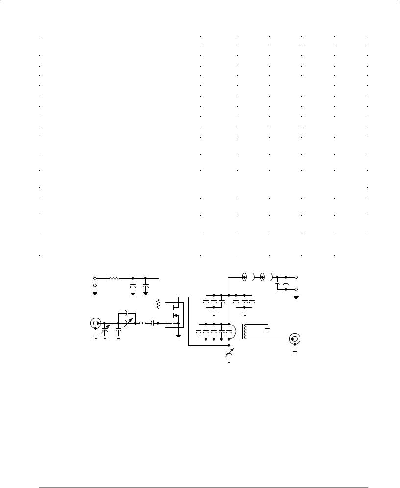
+ |
|
|
|
|
|
|
C20 C21 |
+ |
|
|
|
|
|
|
+ |
||
0±6 V |
R1 |
|
|
|
|
|
50 V |
|
C5 |
C6 |
|
|
L2 |
L3 |
|||
± |
|
|
||||||
|
|
|
|
|
C15 C16 |
C17 C18 |
|
± |
|
|
|
D.U.T. |
C14 |
|
C19 |
|
|
|
|
C4 |
R2 |
|
|
|||
|
|
|
|
|
|
|
|
|
RF |
|
L1 |
C7 |
|
C10 C11 C12 |
C13 |
|
|
|
|
|
|
|
|
|||
INPUT |
C1 |
C3 |
|
C9 |
|
|
|
|
|
C2 |
|
|
|
|
|
RF |
|
|
|
|
|
|
|
|
|
|
|
|
|
|
|
|
T1 |
|
OUTPUT |
C1, C3, C8 Ð Arco 469 |
|
|
|
|
C8 |
|
|
|
|
|
|
|
|
|
|
||
C2 Ð 330 pF |
|
|
|
|
|
|
|
|
C4 Ð 680 pF |
|
|
|
|
|
|
|
|
C5, C19, C20 Ð 0.47 |
mF, RMC Type 2225C |
|
|
|
|
|
||
C6, C7, C14, C15, C16 Ð 0.1 |
mF |
|
|
|
|
|
|
|
C9, C10, C11 Ð 470 pF |
|
|
|
|
|
|
|
|
C12 Ð 1000 pF |
|
|
|
|
R1, R2 Ð 10 Ohms/2W Carbon |
|
||
C13 Ð T wo Unencapsulated 1000 pF Mica, in Series |
|
|
||||||
C17, C18 Ð 0.039 mF |
|
|
|
|
T1 Ð RF Transformer , 1:25 Impedance Ratio. See Motorola |
|||
C21 Ð 10 mF/100 V Electrolytic |
|
|
T1 Ð Application Note AN749, Figure 4 for details. |
|||||
L1 Ð 2 Turns #16 AWG, 1/2 ″ |
ID, 3/8″ Long |
|
|
T1 Ð Ferrite Material: 2 Each, Fair±Rite Products |
||||
L2, L3 Ð Ferrite Beads, Fair±Rite Products Corp. #2673000801 |
T1 Ð |
Corp. #2667540001 |
|
|||||
All capacitors ATC type 100/200 chips or equivalent unless otherwise noted.
Figure 1. 30 MHz Test Circuit
MRF157 |
MOTOROLA RF DEVICE DATA |
2 |
|
|
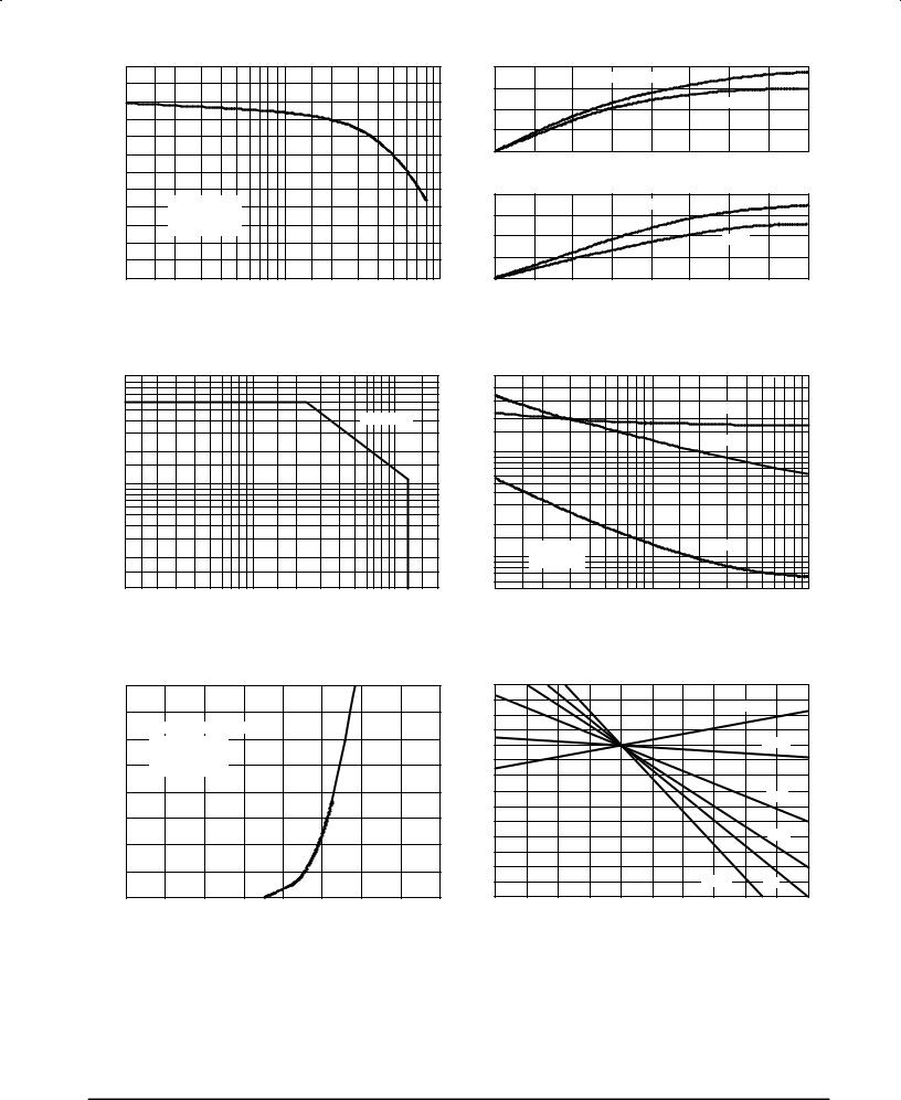
30 |
|
|
|
|
|
|
800 |
|
25 |
|
|
|
|
|
POWER (WATTS) |
600 |
|
|
|
|
|
|
400 |
||
|
|
|
|
|
|
|
||
GAIN (dB) |
20 |
|
|
|
|
|
200 |
|
|
|
|
|
|
0 |
|||
|
|
|
|
|
|
|||
15 |
|
|
|
|
|
|
||
POWER |
|
VDD = 50 V |
|
|
|
|
, OUTPUT |
800 |
10 |
|
|
|
|
600 |
|||
IDQ = 800 mA |
|
|
|
|
||||
|
|
|
|
|
||||
|
|
Pout = 600 W |
|
|
|
|
out |
400 |
|
5 |
|
|
|
|
|
P |
|
|
|
|
|
|
|
|
200 |
|
|
|
|
|
|
|
|
|
|
|
0 |
2 |
5 |
10 |
20 |
50 |
100 |
0 |
|
1 |
|
f, FREQUENCY (MHz)
|
|
VDS = 50 V |
|
|
|
|
|
40 V |
MHz |
|
|
|
|
30 |
0 |
4 |
8 |
12 |
16 |
|
IDQ = 800 mA |
|
|
|
VDS = 50 V |
|
|
|
|
40 V |
MHz |
|
|
80 |
|
|
|
|
|
0 |
40 |
|
80 |
|
Pin, INPUT POWER (WATTS) |
|
|
Figure 2. Power Gain versus Frequency |
Figure 3. Output Power versus Input Power |
|
100 |
|
|
5000 |
|
|
|
|
|
|
(AMPS) |
|
TC = 25°C |
|
2000 |
|
|
|
Ciss |
|
|
|
|
|
|
|
|
|
|
|||
|
|
(pF) |
1000 |
|
|
|
Coss |
|
|
|
DRAINCURRENT |
|
|
CAPACITANCEC, |
|
|
|
|
|
|
|
10 |
|
200 |
|
|
|
|
|
|
||
|
|
|
500 |
|
|
|
|
|
|
|
, |
|
|
|
|
|
|
|
|
|
|
D |
|
|
|
|
V |
= 0 V |
|
Crss |
|
|
I |
|
|
|
|
GS |
|
|
|
|
|
|
|
|
|
100 |
|
|
|
|
|
|
|
|
|
|
f = 1 MHz |
|
|
|
|
||
|
|
|
|
|
|
|
|
|
||
|
1 |
20 |
200 |
50 |
2 |
5 |
10 |
20 |
50 |
100 |
|
2 |
1 |
||||||||
|
V |
, DRAIN±SOURCE VOLTAGE (VOLTS) |
|
|
|
VDS, DRAIN±SOURCE VOLTAGE (VOLTS) |
|
|
||
|
|
DS |
|
|
|
|
|
|
|
|
Figure 4. DC Safe Operating Area |
Figure 5. Capacitance versus Drain Voltage |
IDS, DRAIN CURRENT (AMPS)
40
30
20
10
0
0
TYPICAL DEVICE SHOWN
VDS = 10 V
VGS(th) = 3.5 V
gfs = 24 mhos
2 |
4 |
6 |
VGS, GATE±SOURCE VOLTAGE (VOLTS)
(NORMALIZED) |
1 |
|
|
|
|
16 A |
|
|
1.04 |
|
|
|
|
|
|
|
1.03 |
|
|
|
ID = 20 A |
|
|
|
1.02 |
|
|
|
|
||
|
|
|
|
|
|
||
VOLTAGE |
1.01 |
|
|
|
|
|
|
0.99 |
|
|
|
|
|
||
|
|
|
|
|
|
||
|
0.98 |
|
|
|
|
|
|
GATE±SOURCE |
0.97 |
|
|
|
|
8 A |
|
0.96 |
|
|
|
|
|||
|
|
|
|
|
|||
|
|
|
|
|
|
||
|
0.95 |
|
|
|
|
4 A |
|
|
0.94 |
|
|
|
|
||
|
0.93 |
|
|
|
|
|
|
, |
0.92 |
|
|
|
|
|
|
GS |
0.91 |
|
|
|
0.4 A |
1 A |
|
V |
0.9 |
|
|
|
|
|
|
8 |
0 |
25 |
50 |
75 |
100 |
||
±25 |
|||||||
|
|
|
TC, CASE TEMPERATURE (°C) |
|
|||
Figure 6. Gate Voltage versus Drain Current |
Figure 7. Gate±Source Voltage versus |
|
Case Temperature |
MOTOROLA RF DEVICE DATA |
MRF157 |
|
3 |
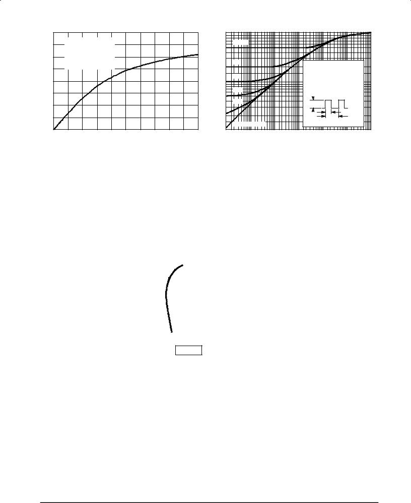
OUTPUTPOWER, (kW) |
4 |
|
|
|
|
|
|
RESISTANCE(NORMALIZED) |
0.05 |
|
|
|
|
|
|
|
|
|
|
|
|
|
|
|
|
1 |
|
|
|
|
|
|
|
|
|
|
|
VDD = 60 V |
|
|
|
|
|
|
|
D = 0.5 |
|
|
|
|
|
|
|
|
|
IDQ = 2 x 800 mA |
|
|
|
|
|
0.5 |
|
|
|
|
|
|
|
|
|
|
3 |
f = 30 MHz |
|
|
|
|
|
|
|
|
|
|
|
|
|
|
|
|
|
t1 |
= 1 ms (See Fig. 9) |
|
|
|
|
|
0.2 |
|
0.2 |
|
R |
(t) = r(t) R |
|
|
|
|
|
t = 10 ms (See Fig. 9) |
|
|
|
|
|
|
|
|
θJC |
° θJC |
|
|
|||
|
|
2 |
|
|
|
|
|
|
|
|
|
|
RθJC = 0.13 |
C/W MAX |
|
||
|
|
|
|
|
|
|
|
|
|
|
0.1 |
|
D CURVES APPLY FOR POWER |
|
|||
|
2 |
|
|
|
|
|
|
|
0.1 |
|
|
PULSE TRAIN SHOWN |
|
||||
|
|
|
|
|
|
|
|
|
|
|
|
||||||
|
|
|
|
|
|
|
|
TRANSIENTTHERMAL |
|
|
|
READ TIME AT t1 |
|
|
|||
P |
0 |
0 |
20 |
40 |
60 |
80 |
100 |
0.01 |
±2 |
±1 |
|
3 |
4 |
||||
|
|
2 |
|||||||||||||||
|
|
|
|
|
|
|
|
|
|
|
0.05 |
|
TJ(pk) ± TC = P(pk) |
RθJC(t) |
|
||
out |
1 |
|
|
|
|
|
|
|
|
|
0.02 |
|
|
P(pk) |
|
|
|
|
|
|
|
|
|
|
|
|
|
|
|
|
|
|
t1 |
|
|
|
|
|
|
|
|
|
|
|
0.02 |
|
|
|
|
|
t2 |
|
|
|
|
|
|
|
|
|
|
|
|
|
SINGLE PULSE |
|
|
DUTY CYCLE, D = t1/t2 |
|
||
|
|
|
|
|
|
|
|
r(t), |
10 |
|
10 |
1 |
10 |
10 |
|
10 |
10 |
|
|
|
Pin, POWER INPUT (WATTS) |
|
|
|
|
|
|
PULSE WIDTH, t (ms) |
|
|
|
||||
|
|
|
|
|
|
|
|
|
|
|
|
|
|||||
Figure 8. Output Power versus Input Power |
Figure 9. Thermal Response versus |
Under Pulse Conditions (2 x MRF157) |
Pulse Width |
Note: Pulse data for this graph was taken in a push±pull circuit similar
Note: to the one shown. However, the output matching network was
Note: modified for the higher level of peak power.
 f = 100 MHz
60
30
 15
15
Zin
 7.5
7.5
 4.0
4.0
 2.0
2.0
Zo = 10 Ω
VDD = 50 V IDQ = 800 mA Pout = 600 W
(VCC ± Vsat)2
Note: To determine ZOL*, use formula |
|
= ZOL* |
2 Po |
Figure 10. Series Equivalent Impedance
MRF157 |
MOTOROLA RF DEVICE DATA |
4 |
|
|
|
|
|
|
|
|
|
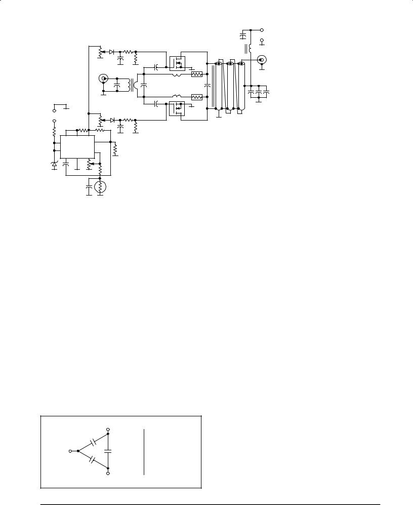
C13 |
+ |
|
|
|
|
|
|
|
|
50 V |
|
|
|
|
|
|
|
|
|
|
± |
|
|
|
D2 |
R10 |
|
|
D.U.T. |
L3 |
|
|
|
R1 |
|
|
|
OUTPUT |
|||
|
|
|
|
|
|
|
|
||
|
|
|
|
C3 |
R12 |
C7 |
|
|
|
|
|
|
|
|
|
|
|
|
|
|
|
|
|
|
|
|
|
R14 |
|
|
|
|
22 pF |
|
|
L1 |
|
C10 |
|
|
|
|
|
C9 |
|
C14 |
|||
|
|
|
|
|
|
|
|
||
|
|
|
|
T1 |
|
|
L2 |
|
C11 |
|
|
|
|
|
|
|
|
|
|
|
|
|
|
|
|
L2 |
|
R15 |
C12 |
|
|
|
|
|
|
|
|
|
|
± |
|
|
D3 |
R11 |
|
C8 |
|
|
|
BIAS 36±50 V |
|
R2 |
|
|
|
T2 |
|
||
+ |
|
|
|
|
|
|
|
||
R5 |
|
|
|
|
D.U.T. |
|
|
||
|
|
|
C4 |
R13 |
|
|
|
||
R4 |
|
|
|
|
|
|
|
||
|
R6 |
|
|
|
|
|
|
|
|
10 |
2 |
|
C1 Ð 1000 pF Ceramic Disc Capacitor |
L3 Ð 10 μH, 10 Turns #12 AWG Enameled Wire on |
|||||
3 |
|
||||||||
12 |
|
4 |
|
C2, C3, C4 Ð 0.1 μF Ceramic Disc Capacitor |
L3 Ð Fair±Rite Products Corp. Ferrite Toroid #5961000401 or Equivalent |
||||
11 |
|
6 5 |
R7 |
C5 Ð 0.01 μF Ceramic Chip Capacitor |
R1 , R2 Ð 1.0K Single Turn Trimpots |
||||
13 |
7 |
|
C6, C12 Ð 0.1 μF Ceramic Chip Capacitor |
R3 Ð 10K Single Turn Trimpot |
|||||
D1 |
C1 R3 |
|
|
C7, C8 Ð Two 2200 pF Ceramic Chip Capacitors in Parallel |
R4 Ð 470 Ohms, 2.0 Watts |
||||
|
R8 |
C7, C8 Ð Each |
|
|
R5 Ð 10 Ohms |
||||
|
|
|
C9 Ð 820 pF Ceramic Chip Capacitor |
R6, R12, R13 Ð 2.0K Ohms |
|||||
|
|
|
|
||||||
|
|
|
|
C10, C11 Ð 1000 pF Ceramic Chip Capacitor |
R7 Ð 10K Ohms |
||||
|
|
|
|
C13 Ð 0.47 μF Ceramic Chip Capacitor or Two Smaller |
R8 Ð Exact Value Depends on Thermistor R9 used |
||||
|
C2 |
|
R9 |
C13 Ð Values in Parallel |
|
R8 Ð (Typically 5.0 ± 10K) |
|||
|
|
|
|
C14 Ð Unencapsulated Mica, 500 V. Two 1000 pF Units |
R9 Ð Thermistor, Keystone RL1009±5820±97±D1 or |
||||
|
|
|
|
C14 Ð in Series, Mounted Under T2 |
|
R9 Ð Equivalent |
|||
|
|
|
|
D1 Ð 1N5357A or Equivalent |
|
R10, R11 Ð 100 Ohms, 1.0W Carbon |
|||
|
|
|
|
D2, D3 Ð 1N4148 or Equivalent. |
|
R14, R15 Ð EMC Technology Model 5308 or KDI |
|||
|
|
|
|
IC1 Ð MC1723 (723) Voltage Regulator |
R14, R15 Ð Pyrofilm PPR 870±150±3 Power Resistors, |
||||
|
|
|
|
L1, L2 Ð 15 ηH, Connecting Wires to R14 and R15, |
R14, R15 Ð 25 Ohms |
||||
|
|
|
|
L1, L2 Ð 2.5 cm Each #20 AWG |
|
T1, T2 Ð 9:1 and 1:9 Impedance Ratio RF Transformers |
|||
Unless otherwise noted, all resistors are 1/2 watt metal film type. All chip capacitors except C13 are ATC type 100/200B or Dielectric Laboratories type C17.
Figure 11. 2.0 to 50 MHz, 1.0 kW Wideband Amplifier
RF POWER MOSFET CONSIDERATIONS
MOSFET CAPACITANCES
The physical structure of a MOSFET results in capacitors between the terminals. The metal oxide gate structure determines the capacitors from gate±to±drain (Cgd), and gate±to± source (Cgs). The PN junction formed during the fabrication of the TMOS FET results in a junction capacitance from drain±to±source (Cds).
These capacitances are characterized as input (Ciss), output (Coss) and reverse transfer (Crss) capacitances on data sheets. The relationships between the interterminal capacitances and those given on data sheets are shown below. The Ciss can be specified in two ways:
1.Drain shorted to source and positive voltage at the gate.
2.Positive voltage of the drain in respect to source and zero volts at the gate. In the latter case the numbers are lower. However, neither method represents the actual operating conditions in RF applications.
|
DRAIN |
|
|
Cgd |
|
GATE |
Cds |
Ciss = Cgd + Cgs |
Coss = Cgd + Cds |
||
|
Cgs |
Crss = Cgd |
|
|
|
|
SOURCE |
|
LINEARITY AND GAIN CHARACTERISTICS
In addition to the typical IMD and power gain data presented, Figure 5 may give the designer additional information on the capabilities of this device. The graph represents the small signal unity current gain frequency at a given drain current level. This is equivalent to fT for bipolar transistors. Since this test is performed at a fast sweep speed, heating of the device does not occur. Thus, in normal use, the higher temperatures may degrade these characteristics to some extent.
DRAIN CHARACTERISTICS
One figure of merit for a FET is its static resistance in the full±on condition. This on±resistance, VDS(on), occurs in the linear region of the output characteristic and is specified under specific test conditions for gate±source voltage and drain current. For MOSFETs, VDS(on) has a positive temperature coefficient and constitutes an important design consideration at high temperatures, because it contributes to the power dissipation within the device.
GATE CHARACTERISTICS
The gate of the TMOS FET is a polysilicon material, and is electrically isolated from the source by a layer of oxide. The input resistance is very high Ð on the order of 10 9 ohms Ð resulting in a leakage current of a few nanoamperes.
Gate control is achieved by applying a positive voltage slightly in excess of the gate±to±source threshold voltage, VGS(th).
MOTOROLA RF DEVICE DATA |
MRF157 |
|
5 |

Gate Voltage Rating Ð Never exceed the gate voltage rating. Exceeding the rated VGS can result in permanent damage to the oxide layer in the gate region.
Gate Termination Ð The gates of these devices are essentially capacitors. Circuits that leave the gate open±circuited or floating should be avoided. These conditions can result in turn±on of the devices due to voltage build±up on the input capacitor due to leakage currents or pickup.
Gate Protection Ð These devices do not have an internal monolithic zener diode from gate±to±source. The addition of an internal zener diode may result in detrimental effects on the reliability of a power MOSFET. If gate protection is required, an external zener diode is recommended.
IMPEDANCE CHARACTERISTICS
Device input and output impedances are normally obtained by measuring their conjugates in an optimized narrow band test circuit. These test circuits are designed and constructed for a number of frequency points depending on the frequency coverage of characterization. For low frequencies the circuits consist of standard LC matching networks including variable capacitors for peak tuning. At increasing power levels the output impedance decreases, resulting in higher RF currents in the matching network. This makes the practicality of output impedance measurements in the manner described questionable at power levels higher than 200±300 W for devices operated at 50 V and 150±200 W for devices operated at 28 V. The physical sizes and values required for the components to withstand the RF currents increase to a point where physical construction of the output matching network gets difficult if not impossible. For this reason the output impedances are not given for high power devices such as the MRF154 and MRF157. However, formulas
like (VDS ± Vsat)2 for ended design 2Pout
or 2((VDS ± Vsat)2)
Pout
obtain reasonably close approximations to actual values.
MOUNTING OF HIGH POWER RF POWER TRANSISTORS
The package of this device is designed for conduction cooling. It is extremely important to minimize the thermal resistance between the device flange and the heat dissipator.
If a copper heatsink is not used, a copper head spreader is strongly recommended between the device mounting surfaces and the main heatsink. It should be at least 1/4″ thick and extend at least one inch from the flange edges. A thin layer of thermal compound in all interfaces is, of course, essential. The recommended torque on the 4 ± 40 mounting screws should be in the area of 4±5 lbs.±inch, and spring type lock washers along with flat washers are recommended.
For die temperature calculations, the D temperature from a corner mounting screw area to the bottom center of the flange is approximately 5°C and 10°C under normal operating conditions (dissipation 150 W and 300 W respectively).
The main heat dissipator must be sufficiently large and have low Rq for moderate air velocity, unless liquid cooling is employed.
CIRCUIT CONSIDERATIONS
At high power levels (500 W and up), the circuit layout becomes critical due to the low impedance levels and high RF currents associated with the output matching. Some of the components, such as capacitors and inductors must also withstand these currents. The component losses are directly proportional to the operating frequency. The manufacturers specifications on capacitor ratings should be consulted on these aspects prior to design.
Push±pull circuits are less critical in general, since the ground referenced RF loops are practically eliminated, and the impedance levels are higher for a given power output. High power broadband transformers are also easier to design than comparable LC matching networks.
EQUIVALENT TRANSISTOR PARAMETER TERMINOLOGY
|
Collector . . . . . . . . . . . . . . . . . |
Drain |
||
|
|
Emitter . . . . . . . . . . . . . . . . . |
Source |
|
|
|
Base . . . . . . . . . . . . . . . . . |
Gate |
|
V(BR)CES . . . . . . . . . . . . . . . . . |
V(BR)DSS |
|||
|
|
VCBO . . . . . . . . . . . . . . . . . |
VDGO |
|
|
|
IC . . . . . . . . . . . . . . . . . |
ID |
|
|
|
ICES . . . . . . . . . . . . . . . . . |
IDSS |
|
|
|
IEBO . . . . . . . . . . . . . . . . . |
IGSS |
|
|
|
VBE(on) . . . . . . . . . . . . . . . . . |
VGS(th) |
|
|
VCE(sat) . . . . . . . . . . . . . . . . . |
VDS(on) |
||
|
|
Cib . . . . . . . . . . . . . . . . . |
Ciss |
|
|
|
Cob . . . . . . . . . . . . . . . . . |
Coss |
|
|
|
hfe . . . . . . . . . . . . . . . . . |
gfs |
|
RCE(sat) = |
|
VCE(sat) . . . . . . . . . . . . . . . . . . |
RDS(on) = |
|
|
IC |
|
||
|
|
|
||
VDS(on)
ID
MRF157 |
MOTOROLA RF DEVICE DATA |
6 |
|
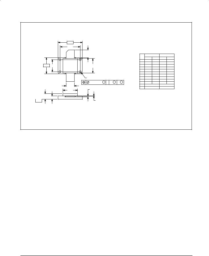
PACKAGE DIMENSIONS
|
±A± |
|
|
|
|
|
|
NOTES: |
|
|
|
|
|
U |
|
|
|
|
|
|
|
|
|
|
|
|
|
|
|
|
|
|
1. DIMENSIONING AND TOLERANCING PER ANSI |
|||||
|
1 |
|
|
|
|
|
|
Y14.5M, 1982. |
|
|
|
|
|
K |
|
|
|
|
|
2. CONTROLLING DIMENSION: INCH. |
|
||||
|
|
|
|
|
|
|
|
INCHES |
MILLIMETERS |
|||
|
|
|
|
|
|
|
|
|
||||
|
|
|
|
|
|
|
|
DIM |
MIN |
MAX |
MIN |
MAX |
|
|
|
|
|
|
|
|
A |
1.490 |
1.510 |
37.85 |
38.35 |
±B± |
V |
N |
|
|
|
|
|
B |
0.990 |
1.010 |
25.15 |
25.65 |
|
|
|
|
|
C |
0.330 |
0.365 |
8.38 |
9.27 |
|||
|
3 |
|
|
|
|
|
|
D |
0.490 |
0.510 |
12.45 |
12.95 |
|
|
|
|
|
|
|
|
E |
0.195 |
0.205 |
4.95 |
5.21 |
|
|
|
|
|
|
|
|
H |
0.045 |
0.055 |
1.14 |
1.39 |
|
|
Q 4 PL |
|
|
|
|
|
J |
0.004 |
0.006 |
0.10 |
0.15 |
|
2 |
|
|
|
|
|
K |
0.425 |
0.500 |
10.80 |
12.70 |
|
|
|
0.25 (0.010) M |
T |
A |
M |
B |
M |
N |
0.890 |
0.910 |
22.87 |
23.11 |
|
D |
Q |
0.120 |
0.130 |
3.05 |
3.30 |
||||||
|
|
|
|
|
|
|
U |
1.250 BSC |
31.75 BSC |
|||
|
N |
H |
|
|
|
|
|
V |
0.750 BSC |
19.05 BSC |
||
|
|
|
|
|
|
|
STYLE 2: |
|
|
|||
|
|
|
|
|
|
|
|
|
|
|
||
C |
|
|
|
|
|
|
|
|
|
PIN 1. DRAIN |
|
|
E |
|
|
|
|
|
|
|
|
2. GATE |
|
||
±T± |
J |
|
|
|
|
|
|
|
3. SOURCE |
|
||
|
|
|
|
|
|
|
|
|
||||
|
|
|
|
|
|
|
|
|
|
|
||
SEATING |
|
|
|
|
|
|
|
|
|
|
|
|
PLANE |
|
|
|
|
|
|
|
|
|
|
|
|
CASE 368±03
ISSUE C
MOTOROLA RF DEVICE DATA |
MRF157 |
|
7 |

Motorola reserves the right to make changes without further notice to any products herein. Motorola makes no warranty, representation or guarantee regarding the suitability of its products for any particular purpose, nor does Motorola assume any liability arising out of the application or use of any product or circuit, and specifically disclaims any and all liability, including without limitation consequential or incidental damages. ªTypicalº parameters can and do vary in different applications. All operating parameters, including ªTypicalsº must be validated for each customer application by customer's technical experts. Motorola does not convey any license under its patent rights nor the rights of others. Motorola products are not designed, intended, or authorized for use as components in systems intended for surgical implant into the body, or other applications intended to support or sustain life, or for any other application in which the failure of the Motorola product could create a situation where personal injury or death may occur. Should Buyer purchase or use Motorola products for any such unintended or unauthorized application, Buyer shall indemnify and hold Motorola and its officers, employees, subsidiaries, affiliates, and distributors harmless against all claims, costs, damages, and expenses, and reasonable attorney fees arising out of, directly or indirectly, any claim of personal injury or death associated with such unintended or unauthorized use, even if such claim alleges that Motorola was negligent regarding the design or manufacture of the part. Motorola and  are registered trademarks of Motorola, Inc. Motorola, Inc. is an Equal Opportunity/Affirmative Action Employer.
How to reach us: |
|
USA / EUROPE: Motorola Literature Distribution; |
JAPAN: Nippon Motorola Ltd.; Tatsumi±SPD±JLDC, Toshikatsu Otsuki, |
P.O. Box 20912; Phoenix, Arizona 85036. 1±800±441±2447 |
6F Seibu±Butsuryu±Center, 3±14±2 Tatsumi Koto±Ku, Tokyo 135, Japan. 03±3521±8315 |
MFAX: RMFAX0@email.sps.mot.com ± TOUCHTONE (602) 244±6609 HONG KONG: Motorola Semiconductors H.K. Ltd.; 8B Tai Ping Industrial Park, |
|
INTERNET: http://Design±NET.com |
51 Ting Kok Road, Tai Po, N.T., Hong Kong. 852±26629298 |
◊ |
MRF157/D |
|
*MRF157/D* |