

MOTOROLA
SEMICONDUCTOR TECHNICAL DATA
Order this document by MRF6401/D
The RF Line
NPN Silicon
RF Power Transistor
The MRF6401 is designed for Class A common emitter, linear power amplifiers in the 1.0 ± 2.0 GHz frequency range. It has been specifically designed for use in Personal Communications Network (PCN) base station and INMARSAT Standard M applications.
•Specified 20 Volts, 1.66 GHz Characteristics: Output Power Ð 0.5 Watts
Gain Ð 10 dB Min Class A Operation
•Specified 20 Volts, 1.88 GHz Characteristics: Output Power Ð 0.5 Watts
Gain Ð 9.0 dB Min Class A Operation
•Circuit Board Photomaster Available by Ordering Document MRF6401PHT/D from Motorola Literature Distribution.
MAXIMUM RATINGS
MRF6401
0.5 W, 1.0 to 2.0 GHz RF LINEAR
POWER TRANSISTOR
CASE 305C±02, STYLE 1
SOE200±PILL
Rating |
|
Symbol |
|
Value |
Unit |
|
|
|
|
|
|
|
|
Collector±Emitter Voltage |
|
VCEO |
|
22 |
Vdc |
|
Collector±Base Voltage |
|
VCBO |
|
45 |
Vdc |
|
Emitter±Base Voltage |
|
VEBO |
|
3.5 |
Vdc |
|
Operating Junction Temperature |
|
TJ |
|
200 |
°C |
|
Total Device Dissipation @ TC = 25°C |
|
PD |
|
5.8 |
Watts |
|
Derate above 25°C |
|
|
|
0.033 |
W/°C |
|
|
|
|
|
|
|
|
Storage Temperature Range |
|
Tstg |
± 65 to +150 |
°C |
||
THERMAL CHARACTERISTICS |
|
|
|
|
|
|
|
|
|
|
|
|
|
Characteristic |
|
Symbol |
|
Max |
Unit |
|
|
|
|
|
|
|
|
Thermal Resistance, Junction to Case (1) |
|
RθJC |
|
30 |
°C/W |
|
ELECTRICAL CHARACTERISTICS (TC = 25°C unless otherwise noted) |
|
|
|
|
|
|
Characteristic |
Symbol |
Min |
Typ |
|
Max |
Unit |
|
|
|
|
|
|
|
OFF CHARACTERISTICS |
|
|
|
|
|
|
|
|
|
|
|
|
|
Collector±Emitter Breakdown Voltage |
V(BR)CER |
28 |
Ð |
|
Ð |
Vdc |
(IC = 10 mAdc, RB = 75 Ω) |
|
|
|
|
|
|
Emitter±Base Breakdown Voltage |
V(BR)EBO |
3.5 |
Ð |
|
Ð |
Vdc |
(IE = 0.25 mAdc) |
|
|
|
|
|
|
Collector±Base Breakdown Voltage |
V(BR)CBO |
45 |
Ð |
|
Ð |
Vdc |
(IC = 1 mAdc) |
|
|
|
|
|
|
(1) Thermal resistance is determined under specified RF operating condition.
REV 1
Motorola, Inc. 1995
ELECTRICAL CHARACTERISTICS Ð continued (TC = 25°C unless otherwise noted)
Characteristic |
Symbol |
Min |
Typ |
Max |
Unit |
|
|
|
|
|
|
ON CHARACTERISTICS
DC Current Gain |
hFE |
20 |
Ð |
120 |
Ð |
(IC = 0.1 Adc, VCE = 5 Vdc) |
|
|
|
|
|
DYNAMIC CHARACTERISTICS
Output Capacitance |
|
Cob |
Ð |
1.4 |
Ð |
pF |
(VCB = 26 V, IE = |
0, f = 1 MHz) |
|
|
|
|
|
FUNCTIONAL TESTS (VCC = 20 V, ICQ = 80 mA)
Common±Emitter Amplifier Power Gain |
Gp |
|
|
|
|
dB |
|
(f = 1660 |
MHz, Pout = 0.5 W) |
|
10 |
|
11 |
Ð |
|
(f = 1880 |
MHz, Pout = 0.5 W) |
|
9 |
|
10 |
Ð |
|
Load Mismatch |
|
|
|
|
|
|
|
(f = 1660 |
MHz, f = 1880 MHz, Pout = 0.5 W, |
ψ |
|
No Degradation in Output Power |
|||
Load VSWR = 20:1, all phase angles at frequency of test) |
|
|
|
|
|
|
|
|
|
|
|
|
|
|
|
Intermodulation Distortion |
IMD |
|
|
|
|
dBc |
|
(Pout = 0.5 W PEP, f1 = 1659.2 MHz, f2 = 1660 MHz) |
|
± 30 |
|
± 35 |
Ð |
|
|
(Pout = 0.5 W PEP, f1 = 1879.2 MHz, f2 = 1880 MHz) |
|
± 30 |
|
± 35 |
Ð |
|
|
|
|
|
R4 |
R5 |
|
R6 |
|
+ |
|
|
|
|
|
|
|
|
|
|
|
|
|
|
|
|
R7 |
VCC |
|
|
|
|
|
Q1 |
|
|
± |
|
|
|
R2 |
R3 |
|
|
R8 |
|
|
|
|
|
|
|
|
||
|
|
|
C9 |
|
|
|
|
|
|
C4 |
C3 |
C10 |
|
TL11 |
|
|
|
|
TL10 |
|
|
C5 |
C6 |
|
C7 |
C8 |
|
|
TL4 |
|
TL6 |
|
|
|
|
|
|
|
|
|
|
|
|
|
|
|
|
TL5 |
|
TL7 |
C2 |
TL9 |
RF |
TL1 |
TL2 |
|
|
|
|
|
|
|
|
|
|
|
|
|
OUTPUT |
||
RF |
|
TP1 |
|
|
|
|
|
|
INPUT |
|
|
|
|
|
|
|
|
C1 |
|
|
|
|
|
|
|
|
|
|
|
|
|
|
|
|
|
|
|
|
DUT |
|
|
|
TL8 |
|
TL3 |
|
TL4 |
|
|
|
|
|
|
C1 |
1.5 pF, ATC Chip Capacitor 100A |
R2 |
470 Ω, Chip Resistor 0805 |
C2 |
3.9 pF, ATC Chip Capacitor 100A |
R3 |
4.7 kΩ, Chip Resistor 0805 |
C3 |
56 pF, ATC Chip Capacitor 100A |
R4 |
8.2 kΩ, Chip Resistor 0805 |
C4, C6, C7, C9 15 nF, Chip Capacitor 0805 |
R5 |
5 kΩ, SMD Potentiometer |
|
C5 |
47 pF, ATC Chip Capacitor 100A |
R6 |
680 Ω, Chip Resistor 0805 |
C8 |
4.7 μF, 35 V, Capacitor |
R7, R8 |
7.5 Ω, Chip Resistor 0805 |
C10 |
10 μF, 16 V, Capacitor |
TL1 to TL11 |
μStrip Lines; See Photomaster |
C11 |
100 pF, ATC Chip Capacitor 100A |
|
Document, MRF6401PHT/D |
Q1 |
Transistor, BCV62 |
TP1 |
μStrip Taper; See Photomaster |
Document, MRF6401PHT/D
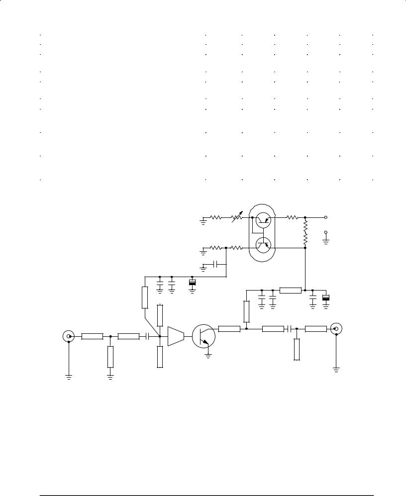
Figure 1. 1600± 2000 MHz Broadband Application Amplifier Schematic
MRF6401 |
MOTOROLA RF DEVICE DATA |
2 |
|

TYPICAL CHARACTERISTICS
|
1000 |
|
|
|
|
|
(mW) |
800 |
|
|
|
|
|
|
|
|
|
|
|
|
POWER |
600 |
|
|
|
|
|
|
|
|
|
|
|
|
, OUTPUT |
400 |
|
|
|
|
|
|
|
|
|
|
|
|
out |
|
|
|
|
|
|
P |
200 |
|
|
|
VCC = 20 V |
|
|
|
|
|
|
||
|
|
|
|
|
IC = 80 mA |
|
|
|
|
|
|
f = 1880 MHz |
|
|
0 |
20 |
40 |
60 |
80 |
100 |
Pin, INPUT POWER (mW)
Figure 2. Output Power versus Input Power
|
40 |
|
|
|
|
|
|
|
|
|
|
|
|
|
|
|
|
|
|
|
10 |
|
|
|
|
S21 |
|
|
|
|
|
|
|
|
|
|
|
|
|
|
|
(dBm) |
20 |
|
|
|
|
(dB) |
5 |
|
|
|
|
|
|
|
|
|
|
|
|
|
|
|
|
|
|||
|
|
|
|
|
|
|
|
|
|
VCC = 20 V |
|
||
,OUTPUT POWER |
|
|
|
|
|
RETURN LOSS |
0 |
|
|
|
|
|
|
0 |
|
|
|
|
|
|
|
|
Pin = 10 dBm |
|
|||
|
|
|
|
|
|
|
|
|
|
IC = 80 mA |
|
||
± 20 |
|
|
|
|
± 5 |
|
|
|
|
|
|
||
|
|
|
|
|
|
|
|
|
|
|
|||
|
|
|
VCC = 20 V |
|
±10 |
|
|
S11 |
|
S11 |
|
||
out |
|
|
|
|
GAIN, |
|
|
|
|
|
|
|
|
|
|
|
IC = 80 mA |
|
|
|
|
|
|
|
|
||
P |
± 40 |
|
|
|
|
|
|
|
|
|
S22 |
||
|
|
|
|
|
±15 |
|
|
|
|
|
|||
|
|
|
|
f = 1880 MHz |
|
S22 |
|
|
|
|
|||
|
|
|
|
|
|
|
|
|
|
||||
|
|
|
|
800 kHz TONE SEPARATION |
|
|
|
|
|
|
|
||
|
± 60 |
5 |
10 |
15 |
20 |
25 |
± 20 |
1600 |
1700 |
1800 |
1900 |
2000 |
2100 |
|
0 |
1500 |
|||||||||||
Pin, INPUT POWER (dBm) |
f, FREQUENCY (MHz) |
Figure 3. Third Order Intercept |
Figure 4. Performance in Broadband Test Fixture |
MOTOROLA RF DEVICE DATA |
MRF6401 |
|
3 |

Table 1. Common Emitter S±Parameters
VCC = 20 V, IC = 80 mA
POLAR S±PARAMETERS IN 50 Ω SYSTEM
f |
S11 |
S21 |
S12 |
|
S22 |
||||
MHz |
|S11| |
é φ |
|S21| |
é φ |
|S12| |
|
é φ |
|S22| |
é φ |
100 |
0.626 |
±118 |
28.4 |
127 |
0.0186 |
|
45 |
0.649 |
± 40 |
200 |
0.718 |
±149 |
17.1 |
106 |
0.0230 |
|
35 |
0.434 |
± 49 |
400 |
0.754 |
±171 |
9.10 |
88 |
0.0271 |
|
35 |
0.303 |
± 53 |
600 |
0.761 |
179 |
6.15 |
77 |
0.0312 |
|
38 |
0.272 |
± 56 |
800 |
0.762 |
171 |
4.65 |
68 |
0.0359 |
|
42 |
0.266 |
± 62 |
1000 |
0.763 |
165 |
3.73 |
60 |
0.0409 |
|
44 |
0.271 |
± 68 |
1200 |
0.758 |
159 |
3.13 |
52 |
0.0469 |
|
44 |
0.286 |
± 75 |
1400 |
0.753 |
155 |
2.60 |
44 |
0.0490 |
|
46 |
0.291 |
± 87 |
1600 |
0.765 |
150 |
2.30 |
39 |
0.0574 |
|
50 |
0.288 |
± 93 |
1800 |
0.769 |
144 |
2.06 |
32 |
0.0665 |
|
49 |
0.303 |
± 97 |
1900 |
0.768 |
142 |
1.98 |
29 |
0.0714 |
|
48 |
0.312 |
±100 |
2000 |
0.767 |
139 |
1.88 |
25 |
0.0756 |
|
48 |
0.322 |
±103 |
VCC = 20 V, IC = 50 mA
POLAR S±PARAMETERS IN 50 Ω SYSTEM
f |
S11 |
S21 |
S12 |
|
S22 |
||||
MHz |
|S11| |
é φ |
|S21| |
é φ |
|S12| |
|
é φ |
|S22| |
é φ |
100 |
0.618 |
±113 |
26.2 |
130 |
0.0195 |
|
45 |
0.678 |
± 36 |
200 |
0.713 |
±145 |
16.2 |
108 |
0.0251 |
|
34 |
0.465 |
± 47 |
400 |
0.758 |
±168 |
8.78 |
89.2 |
0.0288 |
|
32 |
0.331 |
± 51 |
600 |
0.763 |
180 |
5.94 |
78 |
0.0323 |
|
35 |
0.297 |
± 55 |
800 |
0.761 |
169 |
4.49 |
68 |
0.0363 |
|
39 |
0.290 |
± 61 |
1000 |
0.764 |
166 |
3.61 |
60 |
0.0415 |
|
41 |
0.294 |
± 68 |
1200 |
0.758 |
160 |
3.02 |
52 |
0.0467 |
|
42 |
0.310 |
± 75 |
1400 |
0.757 |
155 |
2.52 |
44.5 |
0.0486 |
|
45 |
0.313 |
± 87 |
1600 |
0.768 |
150 |
2.22 |
39 |
0.0566 |
|
48 |
0.311 |
± 92 |
1800 |
0.772 |
145 |
2 |
32 |
0.0655 |
|
48 |
0.328 |
± 97 |
1900 |
0.770 |
142 |
1.91 |
28 |
0.0705 |
|
47 |
0.335 |
±101 |
2000 |
0.772 |
140 |
1.81 |
25 |
0.0745 |
|
47 |
0.345 |
±104 |
GND |
R4 |
R5 |
R6 |
|
|
|
+ VCC |
|
C9 |
|
R7 |
|
|
R8 |
|
|
|
R3 |
|
|
|
|
|
R2 |
|
Q1 |
|
|
|
C8 |
|
|
|
|
||
C10 |
|
|
|
|
|
|
|
|
|
|
|||
|
|
|
|
|
C5 C6 |
C7 |
|||||||
|
|
|
|
|
|
|
|||||||
|
|
|
|
|
|
|
|
|
|
|
|
||
C4 |
|
|
|
|
|
|
|
|
|
|
C11 |
||
|
|
|
|
|
|
|
|
|
|
||||
|
|
|
|
|
|
|
|
|
|
|
|
||
C3 |
|
|
|
|
|
|
|
C2 |
|||||
|
|
|
|
|
|
|
|
|
|||||
|
|
|
|
|
|
|
|
|
|
|
|
|
|
|
|
|
|
|
|
|
|
|
|
|
|
|
|
|
|
|
|
|
|
|
|
|
|
|
|
|
|
|
|
C1 |
|
|
|
|
|
|
|
|
|
||
|
|
|
|
|
|
|
|
|
|
|
|
|
|
Figure 5. Test Circuit Components Layout
MRF6401 |
MOTOROLA RF DEVICE DATA |
4 |
|

PACKAGE DIMENSIONS
|
|
|
|
|
|
|
|
K |
|
|
|
NOTES: |
|
|
|
|
|
|
|
|||
|
|
|
|
|
|
|
|
|
|
|
|
|
|
|
|
|
|
|||||
|
|
|
|
|
|
|
|
|
|
|
|
|
|
|
|
|
|
|
|
|
||
|
|
|
|
|
|
|
|
|
|
|
1 |
|
|
|
|
|
|
|
|
|
||
|
|
|
|
|
|
|
|
|
|
|
|
|
|
|
|
|
|
|
|
|
||
|
|
|
|
|
|
|
|
|
|
|
|
|
|
1. DIMENSIONING AND TOLERANCING PER ANSI |
||||||||
|
|
|
|
|
|
|
|
|
|
|
|
|
|
Y14.5M, 1982. |
|
|
|
|
|
|
||
|
|
|
|
|
|
|
|
|
|
|
|
|
|
|
|
|
|
|
|
|||
|
|
|
|
|
|
|
|
|
|
|
|
|
|
2. CONTROLLING DIMENSION: INCH. |
|
|
|
|||||
|
|
|
|
|
|
|
|
|
|
|
|
|
|
|
|
|
||||||
|
2 |
|
|
|
|
|
|
|
4 |
|
|
INCHES |
MILLIMETERS |
|
||||||||
|
|
|
|
|
|
|
|
|||||||||||||||
|
|
F |
|
|
|
|
|
|
|
|
DIM |
MIN |
MAX |
MIN |
|
MAX |
|
|
||||
|
|
|
|
|
|
|
|
|
|
|
|
|
||||||||||
|
|
|
|
|
|
|
|
|
|
|
|
|
|
|
A |
0.200 |
0.210 |
5.08 |
|
5.33 |
|
|
|
|
|
|
|
|
|
|
|
|
|
|
|
|
|
C |
±±± |
0.125 |
±±± |
|
3.17 |
|
|
|
|
|
|
|
|
|
|
|
|
|
3 |
|
|
|
D |
0.120 |
0.130 |
3.05 |
|
3.30 |
|
|
|
|
|
|
|
|
|
|
|
|
|
|
|
|
F |
0.025 |
0.035 |
0.64 |
|
0.88 |
|
|
|
|
|
|
|
|
|
|
|
|
|
|
|
|
|
|
|
|
|
|||||
|
|
|
|
|
|
|
|
D |
|
|
|
|
H |
0.035 |
0.045 |
0.88 |
|
1.14 |
|
|
||
|
|
|
|
|
|
|
|
|
|
|
||||||||||||
|
|
|
|
|
|
|
|
|
|
|
|
J |
0.004 |
0.006 |
0.11 |
|
0.15 |
|
|
|||
|
|
|
|
|
|
|
|
|
|
|
|
|
|
|
|
|
|
|||||
|
|
|
|
|
|
|
|
|
|
|
|
|
|
|
K |
0.970 |
1.030 |
24.64 |
|
26.16 |
|
|
A 
C
J
H
CASE 305C±02
ISSUE A
STYLE 1:
PIN 1. EMITTER
2.BASE
3.EMITTER
4.COLLECTOR
MOTOROLA RF DEVICE DATA |
MRF6401 |
|
5 |

Motorola reserves the right to make changes without further notice to any products herein. Motorola makes no warranty, representation or guarantee regarding the suitability of its products for any particular purpose, nor does Motorola assume any liability arising out of the application or use of any product or circuit, and specifically disclaims any and all liability, including without limitation consequential or incidental damages. ªTypicalº parameters can and do vary in different applications. All operating parameters, including ªTypicalsº must be validated for each customer application by customer's technical experts. Motorola does not convey any license under its patent rights nor the rights of others. Motorola products are not designed, intended, or authorized for use as components in systems intended for surgical implant into the body, or other applications intended to support or sustain life, or for any other application in which the failure of the Motorola product could create a situation where personal injury or death may occur. Should Buyer purchase or use Motorola products for any such unintended or unauthorized application, Buyer shall indemnify and hold Motorola and its officers, employees, subsidiaries, affiliates, and distributors harmless against all claims, costs, damages, and expenses, and reasonable attorney fees arising out of, directly or indirectly, any claim of personal injury or death associated with such unintended or unauthorized use, even if such claim alleges that Motorola was negligent regarding the design or manufacture of the part. Motorola and  are registered trademarks of Motorola, Inc. Motorola, Inc. is an Equal Opportunity/Affirmative Action Employer.
How to reach us: |
|
USA / EUROPE: Motorola Literature Distribution; |
JAPAN: Nippon Motorola Ltd.; Tatsumi±SPD±JLDC, Toshikatsu Otsuki, |
P.O. Box 20912; Phoenix, Arizona 85036. 1±800±441±2447 |
6F Seibu±Butsuryu±Center, 3±14±2 Tatsumi Koto±Ku, Tokyo 135, Japan. 03±3521±8315 |
MFAX: RMFAX0@email.sps.mot.com ± TOUCHTONE (602) 244±6609 HONG KONG: Motorola Semiconductors H.K. Ltd.; 8B Tai Ping Industrial Park, |
|
INTERNET: http://Design±NET.com |
51 Ting Kok Road, Tai Po, N.T., Hong Kong. 852±26629298 |
◊ |
MRF6401/D |
|
*MRF6401/D* |