

MOTOROLA
SEMICONDUCTOR
TECHNICAL DATA
5 Watt Surmetic 40
Silicon Zener Diodes
This is a complete series of 5 Watt Zener Diodes with tight limits and better operating characteristics that reflect the superior capabilities of silicon-oxide-passivated junctions. All this is in an axial-lead, transfer-molded plastic package that offers protection in all common environmental conditions.
Specification Features:
•Up to 180 Watt Surge Rating @ 8.3 ms
•Maximum Limits Guaranteed on Seven Electrical Parameters
Mechanical Characteristics:
1N5333B through 1N5388B
5 WATT
ZENER REGULATOR
DIODES
3.3±200 VOLTS
CASE: Void-free, transfer-molded, thermosetting plastic
FINISH: All external surfaces are corrosion resistant and leads are readily solderable POLARITY: Cathode indicated by color band. When operated in zener mode, cathode
will be positive with respect to anode
MOUNTING POSITION: Any
WEIGHT: 0.7 gram (approx)
WAFER FAB LOCATION: Phoenix, Arizona
ASSEMBLY/TEST LOCATION: Seoul, Korea
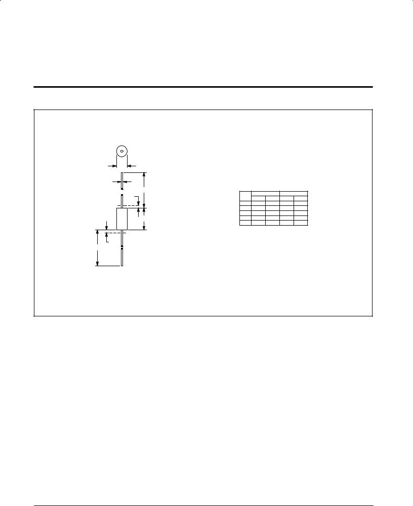
CASE 17 |
PLASTIC |
MAXIMUM RATINGS
Rating |
Symbol |
Value |
Unit |
|
|
|
|
DC Power Dissipation @ TL = 75°C |
PD |
5 |
Watts |
Lead Length = 3/8″ |
|
|
mW/°C |
Derate above 75°C |
|
40 |
|
|
|
|
|
Operating and Storage Junction Temperature Range |
TJ, Tstg |
± 65 to +200 |
°C |
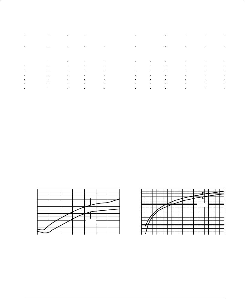
PD , MAXIMUM POWER DISSIPATION (WATTS)
8
|
L = LEAD LENGTH |
L = 1/8″ |
L = TO HEAT SINK |
L = (SEE FIGURE 5) |
6
L = 3/8″
4
L = 1″
2
0
0 |
20 |
40 |
60 |
80 |
100 |
120 |
140 |
160 |
180 |
200 |
|
|
|
TL, LEAD TEMPERATURE (°C) |
|
|
|
|
|||
Figure 1. Power Temperature Derating Curve
5 Watt Surmetic 40 Data Sheet |
Motorola TVS/Zener Device Data |
6-1 |
|

1N5333B through 1N5388B
ELECTRICAL CHARACTERISTICS (TA = 25°C unless otherwise noted, VF = 1.2 Max @ IF = 1 A for all types)
|
|
Nominal |
|
|
|
Max Reverse |
|
|
Maximum |
||
|
|
Zener |
|
Max Zener Impedance |
Leakage Current |
Max |
|
Regulator |
|||
|
|
Voltage |
Test |
|
|
|
|
|
Surge |
Max Voltage |
Current |
|
|
|
|
|
|
|
|||||
|
JEDEC |
VZ @ IZT |
Current |
ZZT @IZT |
ZZK @ IZK = 1 mA |
|
|
|
Current |
Regulation |
IZM |
|
Type No. |
Volts |
IZT |
Ohms |
Ohms |
I |
V |
ir, Amps |
VZ, Volt |
mA |
|
|
(Note 1) |
(Note 2) |
mA |
(Note 2) |
(Note 2) |
R @ |
R |
(Note 3) |
(Note 4) |
(Note 5) |
|
|
μA |
Volts |
|||||||||
|
1N5333B |
3.3 |
380 |
3 |
400 |
300 |
|
1 |
20 |
0.85 |
1440 |
|
1N5334B |
3.6 |
350 |
2.5 |
500 |
150 |
|
1 |
18.7 |
0.8 |
1320 |
|
1N5335B |
3.9 |
320 |
2 |
500 |
50 |
|
1 |
17.6 |
0.54 |
1220 |
|
1N5336B |
4.3 |
290 |
2 |
500 |
10 |
|
1 |
16.4 |
0.49 |
1100 |
|
1N5337B |
4.7 |
260 |
2 |
450 |
5 |
|
1 |
15.3 |
0.44 |
1010 |
|
|
|
|
|
|
|
|
|
|
|
|
|
1N5338B |
5.1 |
240 |
1.5 |
400 |
1 |
|
1 |
14.4 |
0.39 |
930 |
|
1N5339B |
5.6 |
220 |
1 |
400 |
1 |
|
2 |
13.4 |
0.25 |
865 |
|
1N5340B |
6 |
200 |
1 |
300 |
1 |
|
3 |
12.7 |
0.19 |
790 |
|
1N5341B |
6.2 |
200 |
1 |
200 |
1 |
|
3 |
12.4 |
0.1 |
765 |
|
1N5342B |
6.8 |
175 |
1 |
200 |
10 |
|
5.2 |
11.5 |
0.15 |
700 |
|
|
|
|
|
|
|
|
|
|
|
|
|
1N5343B |
7.5 |
175 |
1.5 |
200 |
10 |
|
5.7 |
10.7 |
0.15 |
630 |
|
1N5344B |
8.2 |
150 |
1.5 |
200 |
10 |
|
6.2 |
10 |
0.2 |
580 |
|
1N5345B |
8.7 |
150 |
2 |
200 |
10 |
|
6.6 |
9.5 |
0.2 |
545 |
|
1N5346B |
9.1 |
150 |
2 |
150 |
7.5 |
|
6.9 |
9.2 |
0.22 |
520 |
|
1N5347B |
10 |
125 |
2 |
125 |
5 |
|
7.6 |
8.6 |
0.22 |
475 |
|
|
|
|
|
|
|
|
|
|
|
|
|
1N5348B |
11 |
125 |
2.5 |
125 |
5 |
|
8.4 |
8 |
0.25 |
430 |
|
1N5349B |
12 |
100 |
2.5 |
125 |
2 |
|
9.1 |
7.5 |
0.25 |
395 |
|
1N5350B |
13 |
100 |
2.5 |
100 |
1 |
|
9.9 |
7 |
0.25 |
365 |
|
1N5351B |
14 |
100 |
2.5 |
75 |
1 |
|
10.6 |
6.7 |
0.25 |
340 |
|
1N5352B |
15 |
75 |
2.5 |
75 |
1 |
|
11.5 |
6.3 |
0.25 |
315 |
|
|
|
|
|
|
|
|
|
|
|
|
|
1N5353B |
16 |
75 |
2.5 |
75 |
1 |
|
12.2 |
6 |
0.3 |
295 |
|
1N5354B |
17 |
70 |
2.5 |
75 |
0.5 |
|
12.9 |
5.8 |
0.35 |
280 |
|
1N5355B |
18 |
65 |
2.5 |
75 |
0.5 |
|
13.7 |
5.5 |
0.4 |
265 |
|
1N5356B |
19 |
65 |
3 |
75 |
0.5 |
|
14.4 |
5.3 |
0.4 |
250 |
|
1N5357B |
20 |
65 |
3 |
75 |
0.5 |
|
15.2 |
5.1 |
0.4 |
237 |
|
|
|
|
|
|
|
|
|
|
|
|
|
1N5358B |
22 |
50 |
3.5 |
75 |
0.5 |
|
16.7 |
4.7 |
0.45 |
216 |
|
1N5359B |
24 |
50 |
3.5 |
100 |
0.5 |
|
18.2 |
4.4 |
0.55 |
198 |
|
1N5360B |
25 |
50 |
4 |
110 |
0.5 |
|
19 |
4.3 |
0.55 |
190 |
|
1N5361B |
27 |
50 |
5 |
120 |
0.5 |
|
20.6 |
4.1 |
0.6 |
176 |
|
1N5362B |
28 |
50 |
6 |
130 |
0.5 |
|
21.2 |
3.9 |
0.6 |
170 |
|
|
|
|
|
|
|
|
|
|
|
|
|
1N5363B |
30 |
40 |
8 |
140 |
0.5 |
|
22.8 |
3.7 |
0.6 |
158 |
|
1N5364B |
33 |
40 |
10 |
150 |
0.5 |
|
25.1 |
3.5 |
0.6 |
144 |
|
1N5365B |
36 |
30 |
11 |
160 |
0.5 |
|
27.4 |
3.3 |
0.65 |
132 |
|
1N5366B |
39 |
30 |
14 |
170 |
0.5 |
|
29.7 |
3.1 |
0.65 |
122 |
|
1N5367B |
43 |
30 |
20 |
190 |
0.5 |
|
32.7 |
2.8 |
0.7 |
110 |
|
|
|
|
|
|
|
|
|
|
|
|
|
1N5368B |
47 |
25 |
25 |
210 |
0.5 |
|
35.8 |
2.7 |
0.8 |
100 |
|
1N5369B |
51 |
25 |
27 |
230 |
0.5 |
|
38.8 |
2.5 |
0.9 |
93 |
|
1N5370B |
56 |
20 |
35 |
280 |
0.5 |
|
42.6 |
2.3 |
1 |
86 |
|
1N5371B |
60 |
20 |
40 |
350 |
0.5 |
|
42.5 |
2.2 |
1.2 |
79 |
|
1N5372B |
62 |
20 |
42 |
400 |
0.5 |
|
47.1 |
2.1 |
1.35 |
76 |
|
|
|
|
|
|
|
|
|
|
|
|
|
1N5373B |
68 |
20 |
44 |
500 |
0.5 |
|
51.7 |
2 |
1.5 |
70 |
|
1N5374B |
75 |
20 |
45 |
620 |
0.5 |
|
56 |
1.9 |
1.6 |
63 |
|
1N5375B |
82 |
15 |
65 |
720 |
0.5 |
|
62.2 |
1.8 |
1.8 |
58 |
|
1N5376B |
87 |
15 |
75 |
760 |
0.5 |
|
66 |
1.7 |
2 |
54.5 |
|
1N5377B |
91 |
15 |
75 |
760 |
0.5 |
|
69.2 |
1.6 |
2.2 |
52.5 |
|
|
|
|
|
|
|
|
|
|
|
|
|
1N5378B |
100 |
12 |
90 |
800 |
0.5 |
|
76 |
1.5 |
2.5 |
47.5 |
|
1N5379B |
110 |
12 |
125 |
1000 |
0.5 |
|
83.6 |
1.4 |
2.5 |
43 |
|
1N5380B |
120 |
10 |
170 |
1150 |
0.5 |
|
91.2 |
1.3 |
2.5 |
39.5 |
|
1N5381B |
130 |
10 |
190 |
1250 |
0.5 |
|
98.8 |
1.2 |
2.5 |
36.6 |
|
1N5382B |
140 |
8 |
230 |
1500 |
0.5 |
|
106 |
1.2 |
2.5 |
34 |
|
|
|
|
|
|
|
|
|
|
|
(continued) |
|
Devices listed in bold, italic are Motorola preferred devices. |
|
|
|
|
|
|
||||
|
|
|
|
|
|
|
|
|
|
|
|
5 Watt Surmetic 40 Data Sheet |
|
|
|
|
|
Motorola TVS/Zener Device Data |
|||||
6-2 |
|
|
|
|
|
|
|
|
|
|
|
1N5333B through 1N5388B
ELECTRICAL CHARACTERISTICS Ð continued (TA = 25°C unless otherwise noted, VF = 1.2 Max @ IF = 1 A for all types)
|
Nominal |
|
|
|
Max Reverse |
|
|
Maximum |
||
|
Zener |
|
Max Zener Impedance |
Leakage Current |
Max |
|
Regulator |
|||
|
Voltage |
Test |
|
|
|
|
|
Surge |
Max Voltage |
Current |
|
|
|
|
|
|
|||||
JEDEC |
VZ @ IZT |
Current |
ZZT @IZT |
ZZK @ IZK = 1 mA |
|
|
|
Current |
Regulation |
IZM |
Type No. |
Volts |
IZT |
Ohms |
Ohms |
I |
V |
ir, Amps |
VZ, Volt |
mA |
|
(Note 1) |
(Note 2) |
mA |
(Note 2) |
(Note 2) |
R @ |
R |
(Note 3) |
(Note 4) |
(Note 5) |
|
μA |
Volts |
|||||||||
|
|
|
|
|
|
|
|
|
|
|
1N5383B |
150 |
8 |
330 |
1500 |
0.5 |
|
114 |
1.1 |
3 |
31.6 |
1N5384B |
160 |
8 |
350 |
1650 |
0.5 |
|
122 |
1.1 |
3 |
29.4 |
1N5385B |
170 |
8 |
380 |
1750 |
0.5 |
|
129 |
1 |
3 |
28 |
1N5386B |
180 |
5 |
430 |
1750 |
0.5 |
|
137 |
1 |
4 |
26.4 |
1N5387B |
190 |
5 |
450 |
1850 |
0.5 |
|
144 |
0.9 |
5 |
25 |
1N5388B |
200 |
5 |
480 |
1850 |
0.5 |
|
152 |
0.9 |
5 |
23.6 |
|
|
|
|
|
|
|
|
|
|
|
NOTE 1. TOLERANCE AND TYPE NUMBER DESIGNATION
The JEDEC type numbers shown indicate a tolerance of ±5%.
NOTE 2. ZENER VOLTAGE (VZ) AND IMPEDANCE (ZZT & ZZK)
Test conditions for zener voltage and impedance are as follows: IZ is applied 40 ± 10 ms prior to reading. Mounting contacts are located 3/8″ to 1/2″ from the inside edge of mounting clips to the body of the diode. (TA = 25°C +8, ±2°C).
NOTE 3. SURGE CURRENT (ir)
Surge current is specified as the maximum allowable peak, non-recurrent square-wave current with a pulse width, PW, of 8.3 ms. The data given in Figure 6 may be used to find the maximum surge current for a square wave of any pulse width between 1ms and 1000 ms by plotting the applicable points on logarithmic paper. Examples of this, using the 3.3 V and 200 V zeners, are shown in Figure 7. Mounting contact located as specified in Note 3. (TA = 25°C +8, ±2°C.)
NOTE 4. VOLTAGE REGULATION (DVZ)
Test conditions for voltage regulation are as follows: VZ measurements are made at 10% and then at 50% of the IZ max value listed in the electrical characteristics table. The test current time duration for each VZ measurement is 40 ± 10 ms. (TA = 25°C +8, ±2°C). Mounting contact located as specified in Note 2.
NOTE 5. MAXIMUM REGULATOR CURRENT (IZM)
The maximum current shown is based on the maximum voltage of a 5% type unit, therefore, it applies only to the B-suffix device. The actual IZM for any device may not exceed the value of 5 watts divided by the actual VZ of the device. TL = 75°C at 3/8″ maximum from the device body.
NOTE 6. SPECIALS AVAILABLE INCLUDE:
Nominal zener voltages between the voltages shown and tighter voltage tolerance such as
±1% and ±2%. Consult factory.
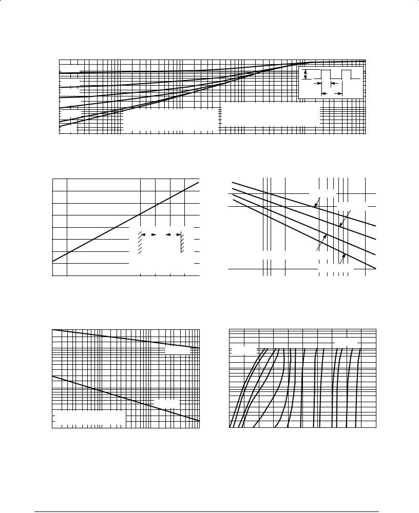
TEMPERATURE COEFFICIENTS
COEFFICIENT |
|
10 |
|
|
|
|
|
|
COEFFICIENT |
|
300 |
|
8 |
|
|
|
|
|
|
|
200 |
||
|
|
|
|
|
|
|
|
|
|||
|
6 |
|
|
|
|
|
|
|
100 |
||
ZT |
|
|
|
|
|
|
ZT |
|
|||
|
|
|
|
|
|
|
50 |
||||
TEMPERATURE |
(mV/°C) @ I |
4 |
|
|
|
|
|
|
TEMPERATURE |
(mV/°C) @ I |
|
|
|
|
|
|
|
30 |
|||||
|
|
|
|
|
|
|
|||||
2 |
|
|
|
|
RANGE |
|
20 |
||||
0 |
|
|
|
|
|
|
|||||
|
|
|
|
|
|
10 |
|||||
|
|
|
|
|
|
|
|
||||
, |
|
|
|
|
|
|
|
|
, |
|
|
Z |
|
±2 |
|
|
|
|
|
|
Z |
|
|
θV |
|
|
|
|
|
|
|
θV |
|
5 |
|
|
|
3 |
4 |
5 |
6 |
7 |
8 |
9 |
10 |
|
|
|
|
|
|
VZ, ZENER VOLTAGE @ IZT (VOLTS) |
|
|
|
|
|||
|
|
|
|
|
|
|
|
RANGE |
|
|
|
0 |
20 |
40 |
60 |
80 |
100 |
120 |
140 |
160 |
180 |
200 |
220 |
|
|
|
VZ, ZENER VOLTAGE @ IZT (VOLTS) |
|
|
||||||
Figure 2. Temperature Coefficient-Range |
Figure 3. Temperature Coefficient-Range |
for Units 3 to 10 Volts |
for Units 10 to 220 Volts |
Devices listed in bold, italic are Motorola preferred devices.
Motorola TVS/Zener Device Data |
5 Watt Surmetic 40 Data Sheet |
|
6-3 |
1N5333B through 1N5388B
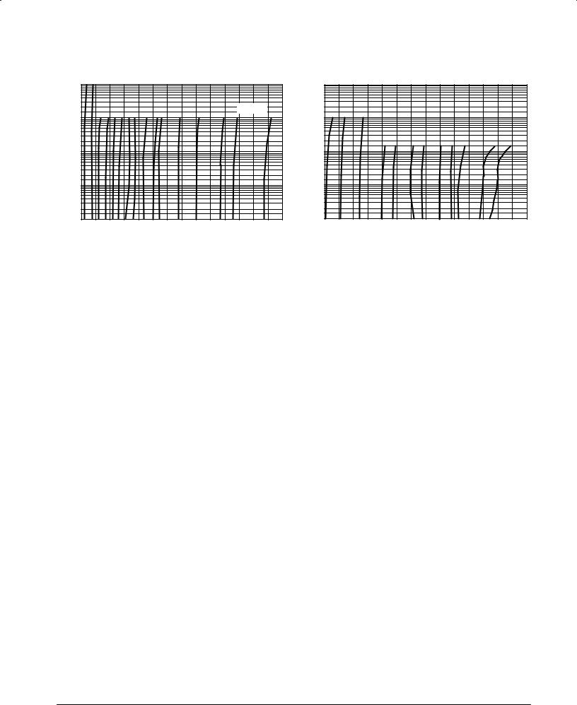
θJL (t, D), TRANSIENT THERMAL RESISTANCE JUNCTION-TO-LEAD (°C/W)
20 |
|
|
|
|
|
|
|
|
|
|
|
|
10 |
D = 0.5 |
|
|
|
|
|
|
|
|
|
|
|
5 |
D = 0.2 |
|
|
|
|
|
|
|
PPK |
t |
|
|
|
|
|
|
|
|
|
|
|
|
1 |
|
|
2 |
D = 0.1 |
|
|
|
|
|
|
|
|
|
t2 |
|
D = 0.05 |
|
|
|
|
|
|
|
|
|
|
|
|
1 |
|
|
|
|
|
DUTY CYCLE, D = t1/t2 |
|
|
|
|||
|
|
|
|
|
|
|
|
|
||||
|
D = 0.01 |
|
|
NOTE: BELOW 0.1 SECOND, THERMAL |
|
SINGLE PULSE |
TJL = θJL(t)PPK |
|
|
|
||
0.5 |
|
|
|
NOTE: RESPONSE CURVE IS APPLICABLE |
REPETITIVE PULSES |
TJL = θJL(t, D)PPK |
|
|
|
|||
0.2 |
D = 0 |
|
|
NOTE: TO ANY LEAD LENGTH (L). |
|
|
|
|
|
|
|
|
|
|
|
|
|
|
|
|
|
|
|
||
|
|
|
|
|
|
|
|
|
|
|
|
|
0.00 |
0.00 |
0.01 |
0.05 |
0.1 |
0.5 |
1 |
5 |
10 |
20 |
50 |
100 |
|
|
1 |
5 |
|
|
t, TIME (SECONDS) |
|
|
|
|
|
|
|
|
|
|
|
|
|
|
|
|
|
|
||
Figure 4. Typical Thermal Response
L, Lead Length = 3/8 Inch
θJL, JUNCTION-TO-LEAD THERMAL RESISTANCE (°C/W)
40
30
20
10
0
0
|
|
|
|
|
|
|
|
|
|
|
|
|
|
|
|
(AMPS) |
40 |
|
|
|
|
|
|
|
|
|
|
|
|
|
|
|
|
|
|
|
|
|
|
|
|
|
|
|
|
|
|
|
|
|
|
|
|
|
|
20 |
|
|
|
|
|
|
|
|
|
|
|
|
|
|
|
|
|
|
|
|
|
|
|
|
|
|
|
|
|
|
|
|
|
|
|
|
|
|
|
|
|
|
|
|
|
|
|
|
|
|
|
|
|
PW |
= 1 |
ms* |
|
|
|
|
|
|
|
|
|
|
|
|
|
|
|
|
|
|
|
|
|
|
|
CURRENT |
10 |
|
|
|
|
|
|
|
|
|
|
|
|
|
|
|
|
|
|
|
|||
|
|
|
|
|
|
|
|
|
|
|
|
|
|
|
|
|
|
|
|
|
|
|
|
|
|
|
|
|
|
|
|
|
|
|
|
|
|
||
|
|
|
|
|
|
|
|
|
|
|
|
|
|
|
|
|
|
|
|
|
|
|
|
|
|
|
|
|
|
|
|
|
|
|
|
|
|
||
|
|
|
|
|
|
|
|
|
|
|
|
|
|
|
|
2 |
|
|
|
|
|
|
|
|
|
|
|
|
|
|
|
|
|
|
|
|
|
|
|
|
|
|
|
|
|
|
|
|
|
|
|
|
|
|
|
|
|
|
|
|
|
|
|
|
|
|
|
|
|
|
|
PW |
= |
8.3 ms* |
|
|
|
||
|
|
|
|
|
|
|
L |
|
|
|
L |
|
|
|
|
SURGE |
4 |
|
|
|
|
|
|
|
|
|
|
|
|
|
|
|
|
|
|
|
|||
|
|
|
|
|
|
|
|
|
|
|
|
|
|
|
|
|
|
|
|
|
|
|
|
|
|
|
|
|
|
|
|
|
|
|
|
||||
|
|
|
|
|
|
|
|
|
|
|
|
|
|
|
|
|
|
|
|
|
|
|
|
|
|
|
|
|
|
|
|
|
|
|
|
||||
|
|
|
|
|
|
|
|
|
|
|
|
|
|
1 |
|
|
|
|
|
|
|
|
|
|
|
|
|
|
|
|
|
|
|
|
|
|
|||
|
|
|
|
|
|
|
|
|
|
|
|
|
|
|
|
|
|
|
|
|
|
|
|
|
|
|
|
|
|
|
|
|
|
|
|
||||
|
|
|
|
|
|
|
|
|
|
|
|
|
|
|
|
|
|
|
|
|
|
|
|
|
|
|
|
|
|
|
|
|
|
|
|
||||
|
|
|
|
|
|
|
|
|
|
|
|
|
|
|
|
|
|
|
|
|
|
|
|
|
|
|
|
|
|
|
|
|
|
|
|||||
|
|
|
|
|
|
|
|
|
|
|
|
|
|
|
|
|
|
|
|
|
|
|
|
|
|
|
|
|
|
|
|
|
|
|
|
|
|
||
|
|
|
|
|
|
|
|
|
|
|
|
|
|
|
|
, PEAK |
0.4 |
|
|
|
|
|
|
|
|
|
|
|
|
|
|
|
|
|
|
|
|
|
|
|
|
|
|
|
|
|
|
|
|
|
|
|
|
|
|
|
|
|
|
|
|
|
|
|
|
|
|
|
|
|
|
|
|
|
|
|
|
||
|
|
|
|
|
|
PRIMARY PATH OF |
|
|
|
|
|
|
|
|
*SQUARE WAVE |
|
|
PW |
= 100 ms* |
|
|
|
|
|
|
||||||||||||||
|
|
|
|
|
|
|
|
i |
|
|
|
|
|
|
|
|
|
|
|
|
|
|
|
|
|
|
|
|
|
|
|
||||||||
|
|
|
|
|
|
|
|
|
|
|
|
|
|
|
|
r |
|
|
|
|
|
|
|
|
|
|
|
|
|
|
|
|
|
|
|
|
|
|
|
|
|
|
|
|
CONDUCTION IS THROUGH |
|
|
0.2 |
|
|
|
|
|
|
|
|
|
|
|
|
|
|
|
|
|
|
|
|
|
|
|||||||||
|
|
|
|
|
|
|
|
|
|
|
|
|
|
|
|
|
|
|
|
|
PW = 1000 ms* |
|
|
|
|
||||||||||||||
|
|
|
|
|
THE CATHODE LEAD |
|
|
0.1 |
|
|
|
|
|
|
|
|
|
|
|
|
|
|
|
|
|
|
|||||||||||||
|
|
|
|
|
|
|
|
|
|
|
|
|
|
|
|
|
|
|
|
|
|
|
|
|
|
|
|
|
|
|
|
|
|
|
|
|
|
|
|
0.2 |
0.4 |
0.6 |
|
0.8 |
|
|
|
1 |
3 |
4 |
6 |
8 |
10 |
20 |
30 |
40 |
60 |
80 100 |
|
200 |
|||||||||||||||||||
|
|
L, LEAD LENGTH TO HEAT SINK (INCH) |
|
|
|
|
|
|
|
|
|
|
|
NOMINAL VZ (V) |
|
|
|
|
|
|
|
||||||||||||||||||
Figure 5. Typical Thermal Resistance |
|
|
|
|
Figure 6. Maximum Non-Repetitive Surge Current |
||||||||||||||||||||||||||||||||||
|
|
|
|
|
|
|
|
|
|
|
|
|
|
|
|
|
|
|
|
|
|
|
|
versus Nominal Zener Voltage |
|
|
|||||||||||||
|
|
|
|
|
|
|
|
|
|
|
|
|
|
|
|
|
|
|
|
|
|
|
|
|
|
(See Note 3) |
|
|
|
|
|
|
|
||||||
|
30 |
|
|
|
(AMPS) |
20 |
|
|
|
10 |
|
|
VZ = 3.3 V |
|
CURRENT |
5 |
|
|
|
|
|
|
|
|
SURGE |
2 |
|
|
|
1 |
|
|
|
|
PEAK |
|
|
|
|
0.5 |
|
|
VZ = 200 V |
|
|
|
|
|
|
, |
|
|
|
|
r |
|
|
|
|
i |
0.2 |
PLOTTED FROM INFORMATION |
|
|
|
|
|||
|
0.1 |
GIVEN IN FIGURE 6 |
|
|
|
|
|
|
|
|
1 |
10 |
100 |
100 |
|
|
|
PW, PULSE WIDTH (ms) |
0 |
|
|
|
|
|
Figure 7. Peak Surge Current versus Pulse Width (See Note 3)
|
|
|
|
|
|
|
|
|
T = 25°C |
|
|
1000 |
TC = 25°C |
|
|
|
|
|
|
|
|
(mA) |
100 |
|
|
|
|
|
|
|
|
|
CURRENT |
|
|
|
|
|
|
|
|
|
|
10 |
|
|
|
|
|
|
|
|
|
|
, ZENER |
1 |
|
|
|
|
|
|
|
|
|
Z |
|
|
|
|
|
|
|
|
|
|
|
|
|
|
|
|
|
|
|
|
|
I |
|
|
|
|
|
|
|
|
|
|
|
0.1 |
|
|
|
|
|
|
|
|
|
|
1 |
2 |
3 |
4 |
5 |
6 |
7 |
8 |
9 |
10 |
VZ, ZENER VOLTAGE (VOLTS)
Figure 8. Zener Voltage versus Zener Current VZ = 3.3 thru 10 Volts
5 Watt Surmetic 40 Data Sheet |
Motorola TVS/Zener Device Data |
6-4 |
|
1N5333B through 1N5388B
|
1000 |
|
|
|
|
|
|
|
(mA) |
|
|
|
|
|
|
T = 25°C |
|
100 |
|
|
|
|
|
|
|
|
CURRENTZENER, |
|
|
|
|
|
|
|
|
10 |
|
|
|
|
|
|
|
|
|
|
|
|
|
|
|
|
|
Z |
1 |
|
|
|
|
|
|
|
I |
|
|
|
|
|
|
|
|
|
0.1 |
|
|
|
|
|
|
|
|
10 |
20 |
30 |
40 |
50 |
60 |
70 |
80 |
VZ, ZENER VOLTAGE (VOLTS)
I Z , ZENER CURRENT (mA)
100
10
1
0.1
80 |
100 |
120 |
140 |
160 |
180 |
200 |
220 |
VZ, ZENER VOLTAGE (VOLTS)
Figure 9. Zener Voltage versus Zener Current VZ = 11 thru 75 Volts
Figure 10. Zener Voltage versus Zener Current VZ = 82 thru 200 Volts
APPLICATION NOTE
Since the actual voltage available from a given zener diode is temperature dependent, it is necessary to determine junction temperature under any set of operating conditions in order to calculate its value. The following procedure is recommended:
Lead Temperature, TL, should be determined from: TL = θLA PD + TA
θLA is the lead-to-ambient thermal resistance and PD is the power dissipation.
Junction Temperature, TJ, may be found from: TJ = TL + TJL
TJL is the increase in junction temperature above the lead temperature and may be found from Figure 4 for a train of power pulses or from Figure 5 for dc power.
TJL = θJL PD
For worst-case design, using expected limits of IZ, limits of PD and the extremes of TJ ( TJ) may be estimated. Changes in voltage, VZ, can then be found from:
V = θVZ TJ
θVZ, the zener voltage temperature coefficient, is found from Figures 2 and 3.
Under high power-pulse operation, the zener voltage will vary with time and may also be affected significantly by the zener resistance. For best regulation, keep current excursions as low as possible.
Data of Figure 4 should not be used to compute surge capability. Surge limitations are given in Figure 6. They are lower than would be expected by considering only junction temperature, as current crowding effects cause temperatures to be extremely high in small spots resulting in device degradation should the limits of Figure 6 be exceeded.
Motorola TVS/Zener Device Data |
5 Watt Surmetic 40 Data Sheet |
|
6-5 |
1N5333B through 1N5388B
Zener Voltage Regulator Diodes Ð Axial Leaded
5 Watt Surmetic 40
B |
|
|
|
|
|
|
|
NOTE: |
|
|
|
|
|
D |
1. LEAD DIAMETER & FINISH NOT CONTROLLED |
|||||
WITHIN DIM F. |
|
|
|
|||
K |
|
|
|
|||
|
INCHES |
MILLIMETERS |
||||
F |
|
|||||
DIM |
MIN |
MAX |
MIN |
MAX |
||
2 |
||||||
A |
0.330 |
0.350 |
8.38 |
8.89 |
||
|
||||||
|
B |
0.130 |
0.145 |
3.30 |
3.68 |
|
|
D |
0.037 |
0.043 |
0.94 |
1.09 |
|
A |
F |
Ð |
0.050 |
Ð |
1.27 |
|
|
K |
1.000 |
1.250 |
25.40 |
31.75 |
|
1 |
|
|
|
|
|
|
F |
|
|
|
|
|
|
K |
|
|
|
|
|
|
CASE 17-02
PLASTIC
(Refer to Section 10 for Surface Mount, Thermal Data and Footprint Information.)
MULTIPLE PACKAGE QUANTITY (MPQ)
REQUIREMENTS
Package Option |
Type No. Suffix |
MPQ (Units) |
|
|
|
Tape and Reel |
RL |
4K |
|
|
|
Tape and Ammo |
TA |
2K |
|
|
|
(Refer to Section 10 for more information on Packaging Specifications.)
Devices listed in bold, italic are Motorola preferred devices.
5 Watt Surmetic 40 Data Sheet |
Motorola TVS/Zener Device Data |
6-6