

MOTOROLA
SEMICONDUCTOR TECHNICAL DATA
Order this document by MR750/D
Designer's Data Sheet
High Current Lead Mounted
Rectifiers
•Current Capacity Comparable to Chassis Mounted Rectifiers
•Very High Surge Capacity
•Insulated Case
Mechanical Characteristics:
•Case: Epoxy, Molded
•Weight: 2.5 grams (approximately)
•Finish: All External Surfaces Corrosion Resistant and Terminal Lead is Readily Solderable
•Lead Temperature for Soldering Purposes: 260°C Max. for 10 Seconds
•Polarity: Cathode Polarity Band
•Shipped 1000 units per plastic bag. Available Tape and Reeled, 800 units per reel by adding a ªRL'' suffix to the part number
•Marking: R750, R751, R752, R754, R758, R760
MAXIMUM RATINGS
MR750
MR751
MR752
MR754
MR756
MR758
MR760
MR754 and MR760 are Motorola Preferred Devices
HIGH CURRENT
LEAD MOUNTED SILICON RECTIFIERS 50±1000 VOLTS DIFFUSED JUNCTION
CASE 194±04
Characteristic |
|
Symbol |
|
MR750 |
MR751 |
|
MR752 |
|
MR754 |
|
MR756 |
MR758 |
MR760 |
Unit |
||||||||
|
|
|
|
|
|
|
|
|
|
|
|
|
|
|
|
|
|
|
|
|
|
|
Peak Repetitive Reverse Voltage |
|
VRRM |
50 |
100 |
|
200 |
400 |
|
600 |
|
800 |
1000 |
|
Volts |
||||||||
Working Peak Reverse Voltage |
|
VRWM |
|
|
|
|
|
|
|
|
|
|
|
|
|
|
|
|
|
|
|
|
DC Blocking Voltage |
|
VR |
|
|
|
|
|
|
|
|
|
|
|
|
|
|
|
|
|
|
|
|
Non±Repetitive Peak Reverse Voltage |
|
VRSM |
60 |
120 |
|
240 |
480 |
|
720 |
|
960 |
1200 |
|
Volts |
||||||||
(Halfwave, single phase, 60 Hz peak) |
|
|
|
|
|
|
|
|
|
|
|
|
|
|
|
|
|
|
|
|
|
|
|
|
|
|
|
|
|
|
|
|
|
|
|
|
|
|
|
|
|
|
|
|
|
RMS Reverse Voltage |
|
VR(RMS) |
35 |
70 |
|
140 |
280 |
|
420 |
|
560 |
700 |
|
Volts |
||||||||
Average Rectified Forward Current |
|
IO |
|
|
|
|
22 (TL = 60°C, 1/8″ Lead Lengths) |
|
|
|
Amps |
|||||||||||
(Single phase, resistive load, 60 Hz) |
|
|
|
|
|
6.0 (TA = 60°C, P.C. Board mounting) |
|
|
|
|
|
|||||||||||
See Figures 5 and 6 |
|
|
|
|
|
|
|
|
|
|
|
|
|
|
|
|
|
|
|
|
|
|
|
|
|
|
|
|
|
|
|
|
|
|
|
|
|
|
|
|
|
|
|
|
|
Non±Repetitive Peak Surge Current |
|
IFSM |
|
|
|
|
|
|
400 (for 1 cycle) |
|
|
|
|
|
|
|
Amps |
|||||
(Surge applied at rated load conditions) |
|
|
|
|
|
|
|
|
|
|
|
|
|
|
|
|||||||
|
|
|
|
|
|
|
|
|
|
|
|
|
|
|
|
|
|
|
|
|
||
|
|
|
|
|
|
|
|
|
|
|
|
|
|
|
|
|
|
|
|
|
|
|
Operating and Storage Junction |
|
TJ, Tstg |
|
|
|
|
|
|
|
65 to +175 |
|
|
|
|
|
|
|
|
°C |
|||
Temperature Range |
|
|
|
|
|
|
|
|
|
|
|
|
|
|
|
|
|
|||||
|
|
|
|
|
|
|
|
|
|
|
|
|
|
|
|
|
|
|
|
|
|
|
|
|
|
|
|
|
|
|
|
|
|
|
|
|
|
|
|
|
|
|
|
|
|
ELECTRICAL CHARACTERISTICS |
|
|
|
|
|
|
|
|
|
|
|
|
|
|
|
|
|
|
|
|
|
|
|
|
|
|
|
|
|
|
|
|
|
|
|
|
|||||||||
Characteristic and Conditions |
|
|
|
|
|
|
Symbol |
|
Max |
|
|
|
Unit |
|||||||||
|
|
|
|
|
|
|
|
|
|
|
|
|
|
|
|
|
||||||
Maximum Instantaneous Forward Voltage Drop |
|
|
|
|
|
|
|
|
|
vF |
|
1.25 |
|
|
|
Volts |
||||||
(iF = 100 Amps, TJ = 25°C) |
|
|
|
|
|
|
|
|
|
|
|
|
|
|
|
|
|
|
|
|
|
|
Maximum Forward Voltage Drop |
|
|
|
|
|
|
|
|
|
|
|
VF |
|
0.90 |
|
|
|
Volts |
||||
(IF = 6.0 Amps, TA = 25°C, 3/8″ leads) |
|
|
|
|
|
|
|
|
|
|
|
|
|
|
|
|
|
|
|
|
||
Maximum Reverse Current |
TJ = 25°C |
|
|
|
|
|
|
|
|
|
IR |
|
25 |
|
|
|
mA |
|||||
(Rated dc Voltage) |
TJ = 100°C |
|
|
|
|
|
|
|
|
|
|
|
|
|
|
1.0 |
|
|
|
mA |
||
Designer's Data for ªWorst Caseº Conditions Ð The Designer's Data Sheet permits the design of most circuits entirely from the information presented. SOA Limit curves Ð representing boundaries on device characteristics Ð are given to facilitate ªworst caseº design.
Preferred devices are Motorola recommended choices for future use and best overall value.
Rev 2
Rectifier Device Data
Motorola, Inc. 1996

MR750 |
MR751 |
MR752 |
MR754 |
MR756 |
MR758 |
MR760 |
|
|
|
|
|
|
|
|
||||||||
|
700 |
|
|
|
|
|
|
|
|
|
(AMP) |
600 |
|
|
|
|
VRRM MAY BE APPLIED BETWEEN |
|
||||
|
500 |
|
° |
|
|
|
|
|
|
|
|
|
|
|
|
|
||||||
|
|
|
|
|
|
|
|
|
|
|
|
|
|
EACH CYCLE OF SURGE. THE TJ |
|
|||||||
|
|
TJ = 25 C |
|
|
|
|
|
|
|
400 |
|
|
|
|
|
|||||||
|
|
|
|
|
|
|
|
|
|
|
CURRENT |
|
|
|
|
NOTED IS TJ PRIOR TO SURGE |
|
|||||
|
|
|
|
|
|
|
|
|
|
|
|
|
|
|
|
|
||||||
|
300 |
|
|
|
|
|
|
MAXIMUM |
|
300 |
|
|
|
|
|
|
|
|
|
|
||
|
200 |
|
|
|
|
|
|
|
|
|
|
|
|
|
|
|
|
|
|
|||
|
|
|
|
|
|
|
|
|
|
|
|
|
|
|
|
|
|
25°C |
|
|
||
|
|
|
|
|
|
|
|
|
|
WAVE |
|
|
|
|
|
|
|
|
|
|
||
|
|
|
TYPICAL |
|
|
|
|
|
|
|
|
|
|
|
|
|
|
° |
|
|
||
|
|
|
|
|
|
|
|
|
|
200 |
|
|
|
|
|
|
|
|
|
|||
|
|
|
|
|
|
|
|
|
|
|
|
|
|
|
25°C |
|
175 C |
|
|
|
||
|
|
|
|
|
|
|
|
|
|
|
, PEAK HALF |
|
|
|
|
TJ = 175°C |
|
|
|
|
|
|
(AMP) |
100 |
|
|
|
|
|
|
|
|
|
|
|
|
|
|
|
|
|
|
|
||
70 |
|
|
|
|
|
|
|
|
|
100 |
|
|
|
|
|
|
|
|
|
|
||
|
|
|
|
|
|
|
|
|
|
|
|
|
|
|
|
|
|
|
|
|||
CURRENT |
50 |
|
|
|
|
|
|
|
|
|
FSM |
80 |
|
|
|
|
|
|
|
|
|
|
30 |
|
|
|
|
|
|
|
|
|
I |
60 |
|
|
|
|
|
|
|
|
|
|
|
FORWARD |
|
|
|
|
|
|
|
|
|
|
1.0 |
2.0 |
|
5.0 |
10 |
|
20 |
50 |
|
100 |
||
|
|
|
|
|
|
|
|
|
|
|
|
|
|
|||||||||
|
|
|
|
|
|
|
|
|
|
|
|
|
|
|
||||||||
20 |
|
|
|
|
|
|
|
|
|
|
|
|
|
|
NUMBER OF CYCLES AT 60 Hz |
|
|
|
||||
|
|
|
|
|
|
|
|
|
|
|
|
|
|
|
|
|
|
|||||
|
|
|
|
|
|
|
|
|
|
|
|
|
|
|
|
|
|
|
|
|
|
|
, INSTANTANEOUS |
10 |
|
|
|
|
|
|
|
|
|
|
|
|
Figure 2. Maximum Surge Capability |
|
|||||||
|
|
|
|
|
|
|
|
|
|
|
|
|
|
|
|
|
|
|
|
|
||
7.0 |
|
|
|
|
|
|
|
|
|
|
|
|
|
|
|
|
|
|
|
|
|
|
5.0 |
|
|
|
|
|
|
|
|
|
|
+0.5 |
|
|
|
|
|
|
|
|
|
|
|
|
|
|
|
|
|
|
|
|
|
|
|
|
|
|
|
|
|
|
|
|
|
|
F |
|
|
|
|
|
|
|
|
|
|
|
|
|
|
|
|
|
|
|
|
|
|
i |
3.0 |
|
|
|
|
|
|
|
|
|
|
|
|
|
|
|
|
|
|
|
|
|
|
|
|
|
|
|
|
|
|
|
|
0 |
|
|
|
|
|
|
|
|
|
|
|
|
|
|
|
|
|
|
|
|
|
|
°C) |
|
|
|
|
|
|
|
|
|
|
|
|
2.0 |
|
|
|
|
|
|
|
|
|
|
|
|
|
|
|
|
|
|
|
|
|
|
|
|
|
|
|
|
|
|
|
|
(mV/ |
±0.5 |
|
|
|
TYPICAL RANGE |
|
|
|
|||
|
|
|
|
|
|
|
|
|
|
|
COEFFICIENT |
|
|
|
|
|
|
|
|
|
|
|
|
1.0 |
|
|
|
|
|
|
|
|
|
|
|
|
|
|
|
|
|
|
|
|
|
|
0.7 |
|
|
|
|
|
|
|
|
|
±1.0 |
|
|
|
|
|
|
|
|
|
|
|
|
|
|
|
|
|
|
|
|
|
|
|
|
|
|
|
|
|
|
|
|
||
|
0.5 |
|
|
|
|
|
|
|
|
|
|
|
|
|
|
|
|
|
|
|
|
|
|
|
|
|
|
|
|
|
|
|
|
|
|
|
|
|
|
|
|
|
|
|
|
|
|
|
|
|
|
|
|
|
|
|
|
±1.5 |
|
|
|
|
|
|
|
|
|
|
|
0.3 |
|
|
|
|
|
|
|
|
|
|
|
|
|
|
|
|
|
|
|
|
|
|
0.2 |
|
|
|
|
|
|
|
|
|
|
±2.0 |
0.2 |
0.5 |
1.0 |
2.0 |
5.0 |
10 |
20 |
50 |
100 |
200 |
|
0.6 |
0.8 |
1.0 |
1.2 |
1.4 |
1.6 |
1.8 |
2.0 |
2.2 |
2.4 |
2.6 |
|
||||||||||
|
|
vF, INSTANTANEOUS FORWARD VOLTAGE (VOLTS) |
|
|
|
iF, INSTANTANEOUS FORWARD CURRENT (AMP) |
|
|
||||||||||||||
Figure 1. Forward Voltage |
Figure 3. Forward Voltage Temperature Coefficient |
THERMAL RESISTANCE (°C/W)
R θJL(t) , JUNCTION±TO±LEAD TRANSIENT
20 |
|
|
|
|
|
|
|
|
|
|
|
|
|
|
10 |
L |
|
L |
|
|
|
|
|
|
|
|
|
1/2º |
|
|
|
|
|
|
|
|
|
|
|
3/8º |
|
|||
|
|
|
|
|
|
|
|
|
|
|
|
|
|
|
5.0 |
|
|
|
|
|
|
|
|
|
|
|
|
1/4º |
|
|
|
|
|
|
|
|
|
|
|
|
|
|
|
|
3.0 |
|
HEAT SINK |
|
|
|
|
|
|
|
|
|
|
1/8º |
|
|
|
|
|
|
|
|
|
|
|
|
|
|
|
|
2.0 |
|
|
|
|
|
|
|
Both leads to heat sink, with lengths as shown. Variations in RqJL(t) |
|
|||||
|
|
|
|
|
|
|
|
below 2.0 seconds are independent of lead connections of 1/8 inch |
|
|||||
|
|
|
|
|
|
|
|
or greater, and vary only about ±20% from the values shown. Values |
|
|||||
1.0 |
|
|
|
|
|
|
|
for times greater than 2.0 seconds may be obtained by drawing a |
|
|||||
|
|
|
|
|
|
|
|
curve, with the end point (at 70 seconds) taken from Figure 8, or |
|
|||||
0.5 |
|
|
|
|
|
|
|
calculated from the notes, using the given curves as a guide. Either |
|
|||||
|
|
|
|
|
|
|
typical or maximum values may be used. For RqJL(t) values at pulse |
|
||||||
0.3 |
|
|
|
|
|
|
|
widths less than 0.1 second, the above curve can be extrapolated |
|
|||||
|
|
|
|
|
|
|
down to 10 μs at a continuing slope. |
|
|
|
||||
0.2 |
|
|
|
|
1.0 |
2.0 |
|
5.0 |
|
10 |
20 |
|
50 |
|
0.1 |
0.2 |
0.3 |
0.5 |
0.7 |
3.0 |
7.0 |
30 |
70 |
||||||
t, TIME (SECONDS)
Figure 4. Typical Transient Thermal Resistance
2 |
Rectifier Device Data |
|
|
|
|
|
|
|
|
|
|
MR750 |
|
MR751 |
MR752 |
MR754 |
MR756 |
MR758 |
MR760 |
|||||||||
,AVERAGE FORWARD CURRENT (AMPS) |
28 |
|
|
|
|
|
|
RESISTIVE INDUCTIVE |
, AVERAGE FORWARD CURRENT (AMPS) |
|
7.0 |
|
|
|
RθJA = 25°C/W |
|
|
|
|
|
|
|||||
|
L = 1/8º |
|
|
|
|
|
|
|
|
|
|
|
|
|
|
|
|
|||||||||
24 |
|
|
|
|
|
|
LOADS |
|
|
|
6.0 |
|
|
|
|
SEE NOTE |
|
|
|
|
|
|
||||
|
|
|
|
|
|
|
|
|
|
|
|
|
|
|
|
|
|
|
|
|||||||
20 |
1/4º |
|
|
|
|
BOTH LEADS TO HEAT |
|
|
5.0 |
|
|
|
|
RESISTIVE INDUCTIVE LOADS |
|
|||||||||||
|
|
|
|
|
|
|
|
|
|
|
|
|
|
F |
& 3 |
F |
|
|||||||||
|
|
|
|
|
|
|
SINK WITH LENGTHS |
|
|
|
|
|
|
|
CAPACITANCE LOADS ± 1 |
|
|
|
||||||||
|
|
3/8º |
|
|
|
|
|
|
|
|
|
|
|
|
|
|
I(pk) = 5 Iavg |
|
||||||||
16 |
|
|
|
|
|
AS SHOWN |
|
|
|
4.0 |
|
|
|
|
|
|
|
|
||||||||
|
|
|
|
|
|
|
|
|
|
|
|
|
|
|
|
|
|
|
|
I(pk) = 10 Iavg |
|
|||||
12 |
|
|
5/8º |
|
|
|
|
|
|
|
|
3.0 |
|
|
|
|
|
|
|
I(pk) = 20 Iavg |
|
|||||
|
|
|
|
|
|
|
|
|
|
|
|
|
|
|
|
|
|
|
|
|
|
|||||
|
|
|
|
|
|
|
|
|
|
|
|
RθJA = 40°C/W |
|
|
|
|
|
|
|
|
|
|||||
8.0 |
|
|
|
|
|
|
|
|
|
|
|
2.0 |
|
|
|
|
f = 60 Hz |
|
|
|
||||||
|
|
|
|
|
|
|
|
|
|
|
|
SEE NOTE |
|
|
|
|
|
|
|
|||||||
|
|
|
|
|
|
|
|
|
|
|
|
|
|
|
|
|
|
|
|
|
||||||
|
|
|
|
|
|
|
|
|
|
|
|
|
|
|
|
|
|
|
|
|
|
|
||||
4.0 |
|
|
|
|
|
|
|
|
|
|
|
1.0 |
|
|
6F (IPK/IAVE = 6.28) |
|
|
|
|
|
|
|
||||
F(AV) |
|
|
|
|
|
|
|
|
|
|
|
F(AV) |
|
|
|
|
|
|
|
|
|
|
||||
0 |
|
|
|
|
|
|
|
|
|
|
0 |
|
|
|
|
|
|
|
|
|
|
|
|
|||
I |
20 |
40 |
60 |
80 |
100 |
120 |
140 |
160 |
180 |
200 |
I |
|
20 |
40 |
60 |
80 |
100 |
120 |
140 |
160 |
180 |
200 |
|
|||
|
0 |
|
|
0 |
|
|||||||||||||||||||||
|
|
|
|
TL, LEAD TEMPERATURE (°C) |
|
|
|
|
|
|
|
|
TA, AMBIENT TEMPERATURE (°C) |
|
|
|
|
|
||||||||
Figure 5. Maximum Current Ratings |
Figure 6. Maximum Current Ratings |
|
32 |
|
|
|
|
|
|
|
|
|
|
|
|
|
|
|
|
(WATTS) |
|
CAPACITANCE |
LOADS |
|
|
|
|
|
|
|
|
|
|
|
|||
|
|
|
|
|
|
|
|
|
|
|
|
|
|||||
28 |
|
|
I(pk) |
= 5 Iavg |
|
|
|
|
|
|
|
|
6F |
|
|
||
|
|
|
|
|
|
|
|
|
|
|
|
|
|||||
|
|
|
|
|
|
|
|
|
|
|
|
|
|
|
|
|
|
DISSIPATION |
24 |
|
|
|
10 Iavg |
|
|
|
|
|
|
1 |
F |
& 3 |
F |
|
|
|
|
|
|
|
|
|
|
|
|
|
|||||||
|
|
|
|
|
|
|
|
|
|
|
|
|
|
|
|
||
|
20 |
|
|
|
|
|
|
|
|
|
|
|
|
|
|
|
|
|
|
|
|
20 Iavg |
|
|
|
|
|
|
|
|
|
|
|
||
|
|
|
|
|
|
|
|
|
|
|
|
|
|
|
|
||
, POWER |
16 |
|
|
|
|
|
|
|
|
|
|
|
|
|
|
|
|
|
|
|
|
|
|
|
|
|
|
|
|
|
|
|
|
||
12 |
|
|
|
|
|
|
|
|
|
|
|
|
|
|
|
|
|
8.0 |
|
|
|
|
|
|
|
RESISTIVE |
± INDUCTIVE |
LOADS |
|
||||||
F(AV) |
4.0 |
|
|
|
|
|
|
|
|
|
|
|
|
|
|
|
|
P |
|
|
|
|
|
|
|
|
|
|
|
|
|
|
|
|
|
|
0 |
|
|
|
|
|
|
|
|
|
|
|
|
|
|
|
|
|
|
4.0 |
8.0 |
12 |
16 |
20 |
24 |
28 |
32 |
||||||||
|
0 |
||||||||||||||||
IF(AV), AVERAGE FORWARD CURRENT (AMPS)
Figure 7. Power Dissipation
|
|
40 |
|
|
|
|
|
|
|
|
|
|
35 |
SINGLE LEAD TO HEAT SINK, |
|
|
|
|
|
||
RESISTANCE, |
C/W) |
INSIGNIFICANT HEAT FLOW |
|
|
|
|
|
|||
|
|
|
|
|
|
|||||
30 |
THROUGH OTHER LEAD |
|
|
|
|
|
||||
° |
|
|
|
|
|
|
|
|
||
25 |
|
|
|
|
|
|
|
|
||
|
|
|
|
|
|
|
|
|
||
, THERMAL |
|
20 |
|
|
|
|
|
|
|
|
|
15 |
|
|
|
|
|
|
|
|
|
|
|
|
|
|
|
|
|
|
|
|
JL |
10 |
|
|
|
|
|
|
|
|
|
θ JUNCTION±TO±LEAD( |
|
|
|
|
BOTH LEADS TO HEAT |
|
||||
|
|
|
|
|
|
|||||
R |
|
|
|
|
|
|
|
|||
|
5.0 |
|
|
|
|
SINK, EQUAL LENGTH |
|
|||
|
|
|
|
|
|
|
||||
|
|
|
|
|
|
|
|
|
|
|
|
|
0 |
|
|
|
|
|
|
|
|
|
|
0 |
1/8 |
1/4 |
3/8 |
1/2 |
5/8 |
3/4 |
7/8 |
1.0 |
L, LEAD LENGTH (INCHES)
Figure 8. Steady State Thermal Resistance
NOTES
THERMAL CIRCUIT MODEL
(For Heat Conduction Through The Leads)
|
|
|
RθS(A) |
|
RθL(A) |
|
RθJ(A) |
|
|
RθJ(K) |
|
RθL(K) |
|
RθS(K) |
|
|
|||
|
|
|
|
|
|
|
|
|
|
|
|||||||||
|
|
|
|
|
|
|
|
||||||||||||
|
|
|
TA(A) |
|
|
|
|
|
|
|
|
|
|
|
TA(K) |
|
|
|
|
|
|
|
|
|
|
|
|
|
PF |
|
|
|
|
|
|
|
|||
|
|
|
|
|
|
|
|
|
|
|
|
|
|
|
|||||
|
|
|
|
|
|
|
|
|
|
|
|
|
|
|
|||||
|
|
|
|
|
|
|
|
|
|
|
|
|
|
|
|
|
|
|
|
|
|
|
|
TL(A) |
T |
C(A) |
TJ |
|
|
T |
C(K) |
T |
L(K) |
|
|
||||
|
|
|
|
|
|
|
|
|
|
|
|
|
|
|
|
|
|
|
|
Use of the above model permits junction to lead thermal resistance for any mounting configuration to be found. Lowest values occur when one side of the rectifier is brought as close as possible to the heat sink as shown below. Terms in the model signify:
TA = Ambient Temperature |
TC = Case Temperature |
TL = Lead Temperature |
TJ = Junction Temperature |
RqS = Thermal Resistance, Heat Sink to Ambient
RqL = Thermal Resistance, Lead to Heat Sink
RqJ = Thermal Resistance, Junction to Case
PF = Power Dissipation
(Subscripts A and K refer to anode and cathode sides, respectively.)
Values for thermal resistance components are:
RqL = 40°C/W/in. Typically and 44°C/W/in Maximum.
RqJ = 2°C/W typically and 4°C/W Maximum.
Since RqJ is so low, measurements of the case temperature, TC, will be approximately equal to junction temperature in practical lead mounted applications. When used as a 60 Hz rectifierm the slow thermal response
holds TJ(PK) close to TJ(AVG). Therefore maximum lead temperature may be found from: TL = 175°±RθJL PF. PF may be found from Figure 7.
The recommended method of mounting to a P.C. board is shown on the sketch, where RθJA is approximately 25°C/W for a 1±1/2º x 1±1/2º copper surface area. Values of 40°C/W are typical for mounting to terminal strips or P.C. boards where available surface area is small.
 Board Ground Plane
Recommended mounting for half wave circuit
Rectifier Device Data |
3 |

MR750 |
MR751 |
MR752 |
MR754 |
MR756 |
MR758 |
|
MR760 |
|
|
|
|
|
|
|
|
|
|||||||||
|
100 |
|
|
|
|
|
|
|
|
|
|
|
|
30 |
|
|
|
|
|
|
|
|
|
|
|
(%) |
70 |
|
|
|
|
|
|
|
T |
= 25°C |
|
s) |
20 |
|
|
|
|
|
|
|
|
|
|
|
|
|
|
|
|
|
|
|
|
m |
|
|
|
|
|
|
|
|
|
|
|
|
|||||
|
|
|
|
|
|
|
J |
|
|
|
( |
|
|
|
|
|
|
|
|
|
|
|
|
||
RELATIVE EFFICIENCY |
|
|
|
|
|
|
|
|
|
|
|
|
, REVERSE RECOVERY TIME |
10 |
|
|
|
|
|
|
|
TJ = 25°C |
|
|
|
50 |
|
|
|
TJ = 175°C |
|
|
|
|
|
|
|
|
|
|
|
|
|
|
|
|
|||||
|
|
|
|
|
|
|
|
|
|
|
|
|
|
|
|
|
|
|
|
||||||
|
|
|
|
|
|
|
|
|
|
|
7.0 |
|
IF = 5 A |
|
|
|
|
|
|
|
|
||||
|
|
|
|
|
|
|
|
|
|
|
|
|
|
|
|
|
|
|
|
|
|||||
|
CURRENT INPUT WAVEFORM |
|
|
|
|
|
|
5.0 |
|
|
3 A |
|
|
|
|
|
|
|
|
||||||
|
|
|
|
|
|
|
|
|
1 A |
|
|
|
|
|
|
|
|
||||||||
|
|
|
|
|
|
|
|
|
|
|
|
|
|
|
|
|
|
|
|
|
|
|
|||
30 |
|
|
|
|
|
|
|
|
|
|
|
3.0 |
|
|
IF |
|
|
|
|
|
|
|
|
||
|
|
|
|
|
|
|
|
|
|
|
|
2.0 |
|
0 |
|
|
|
|
|
|
|
|
|
||
|
|
|
|
|
|
|
|
|
|
|
|
|
IR |
|
|
|
|
|
|
|
|
|
|||
|
|
|
|
|
|
|
|
|
|
|
|
|
rr |
|
|
|
trr |
|
|
|
|
|
|
|
|
|
|
|
|
|
|
|
|
|
|
|
|
|
t |
|
|
|
|
|
|
|
|
|
|
|
|
|
|
|
|
|
|
|
|
|
|
|
|
|
|
|
|
|
|
|
|
|
|
|
|
|
|
|
20 |
|
|
|
7.0 |
10 |
20 |
30 |
|
50 |
|
|
|
1.0 |
|
|
|
|
0.7 |
1.0 |
2.0 |
3.0 |
5.0 |
|
|
|
1.0 |
2.0 |
3.0 |
5.0 |
|
70 |
100 |
|
|
0.1 |
0.2 |
0.3 |
0.5 |
7.0 |
10 |
||||||||||
|
|
|
REPETITION FREQUENCY (kHz) |
|
|
|
|
|
|
|
IR/IF, RATIO OF REVERSE TO FORWARD CURRENT |
|
|
||||||||||||
Figure 9. Rectification Efficiency |
Figure 10. Reverse Recovery Time |
|
1000 |
|
|
|
|
|
|
|
|
|
|
1.0 |
|
700 |
|
|
|
|
|
|
|
|
|
s) |
|
|
500 |
|
|
|
|
|
|
|
|
|
0.7 |
|
|
|
|
|
|
|
|
|
TJ = 25°C |
|
m |
||
|
|
|
|
|
|
|
|
|
|
( |
|
|
|
300 |
|
|
|
|
|
|
|
|
TIME |
|
|
(pF) |
|
|
|
|
|
|
|
|
|
0.5 |
||
200 |
|
|
|
|
|
|
|
|
|
|||
|
|
|
|
|
|
|
|
|
|
|||
C, CAPACITANCE |
|
|
|
|
|
|
|
|
|
FORWARD RECOVERY |
|
|
100 |
|
|
|
|
|
|
|
|
|
0.3 |
||
70 |
|
|
|
|
|
|
|
|
|
|||
|
|
|
|
|
|
|
|
|
|
|||
50 |
|
|
|
|
|
|
|
|
|
0.2 |
||
30 |
|
|
|
|
|
|
|
|
|
|||
|
|
|
|
|
|
|
|
|
|
|||
20 |
|
|
|
|
|
|
|
|
|
|
||
|
|
|
|
|
|
|
|
|
|
, |
|
|
|
|
|
|
|
|
|
|
|
|
fr |
|
|
|
|
|
|
|
|
|
|
|
|
|
t |
|
|
10 |
|
|
5.0 |
7.0 |
10 |
20 |
30 |
50 |
70 |
100 |
0.1 |
|
1.0 |
2.0 |
3.0 |
|
uf |
|
|
TJ = 25°C |
|
|
|
|
|
|
|
|
tfr |
ufr |
|
|
|
|
|
|
|
|
ufr = 1.0 V |
|
|
|
|
|
ufr = 2.0 V |
|
1.0 |
2.0 |
3.0 |
5.0 |
7.0 |
10 |
VR, REVERSE VOLTAGE (VOLTS)
Figure 11. Junction Capacitance
RS |
|
RL |
VO |
Figure 13. Single±Phase Half±Wave
Rectifier Circuit
The rectification efficiency factor σ shown in Figure 9 was calculated using the formula:
V2o(dc)
(1)
σ + P(dc) RL . V2o(dc) .
P(rms) + V2o(rms) 100% + V2o(ac) ) V2o(dc) 100%
RL
For a sine wave input Vm sin (wt) to the diode, assumed lossless, the maximum theoretical efficiency factor becomes:
V2m
p2RL |
4 |
|
|
|
σ(sine) + V2m .100% + |
.100% + 40.6% |
(2) |
||
π2 |
4RL
IF, FORWARD PULSE CURRENT (AMP)
Figure 12. Forward Recovery Time
For a square wave input of amplitude Vm, the efficiency factor becomes:
|
|
|
V2m |
|
|
||
σ |
|
|
2RL . |
|
|||
|
+ |
|
|
|
100% + 50% |
(3) |
|
(square) |
2 |
m |
|||||
|
|
V |
|
|
|||
RL
(A full wave circuit has twice these efficiencies)
As the frequency of the input signal is increased, the reverse recovery time of the diode (Figure 10) becomes significant, resulting in an increasing ac voltage component across RL which is opposite in polarity to the forward current, thereby reducing the value of the efficiency factor σ, as shown on Figure 9.
It should be emphasized that Figure 9 shows waveform efficiency only; it does not provide a measure of diode losses. Data was obtained by measuring the ac component of Vo with a true rms ac voltmeter and the dc component with a dc voltmeter. The data was used in Equation 1 to obtain points for Figure 9.
4 |
Rectifier Device Data |
MR750 MR751 MR752 MR754 MR756 MR758 MR760
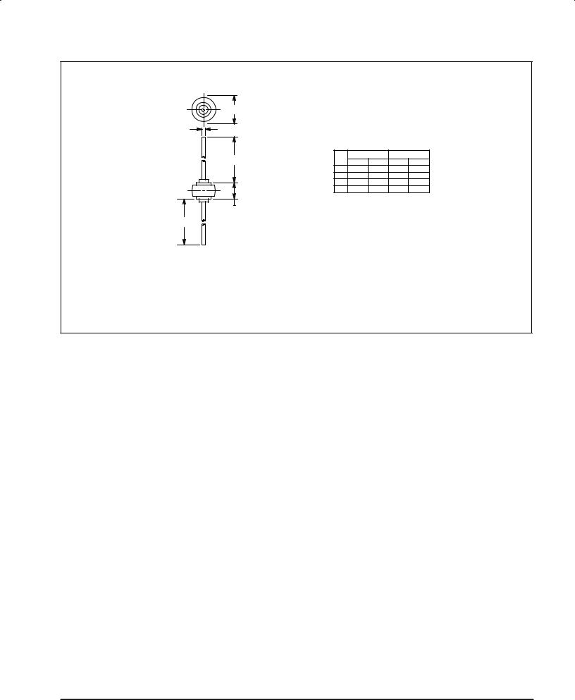
PACKAGE DIMENSIONS
A
D |
NOTES: |
|
|
|
|
|
|
|
|
|
|
1 |
1. CATHODE SYMBOL ON PACKAGE. |
|
|||
|
|
|
|
|
|
K |
|
MILLIMETERS |
INCHES |
||
DIM |
MIN |
MAX |
MIN |
MAX |
|
|
A |
8.43 |
8.69 |
0.332 |
0.342 |
|
B |
5.94 |
6.25 |
0.234 |
0.246 |
|
D |
1.27 |
1.35 |
0.050 |
0.053 |
|
E |
25.15 |
25.65 |
0.990 |
1.010 |
|
B |
|
|
|
|
|
STYLE 1: |
|
|
|
|
K |
PIN 1. CATHODE |
|
|
||
|
2. ANODE |
|
|
|
|
2 |
|
|
|
|
|
CASE 194±04
ISSUE F
Rectifier Device Data |
5 |

MR750 MR751 MR752 MR754 MR756 MR758 MR760
Motorola reserves the right to make changes without further notice to any products herein. Motorola makes no warranty, representation or guarantee regarding the suitability of its products for any particular purpose, nor does Motorola assume any liability arising out of the application or use of any product or circuit, and specifically disclaims any and all liability, including without limitation consequential or incidental damages. ªTypicalº parameters which may be provided in Motorola data sheets and/or specifications can and do vary in different applications and actual performance may vary over time. All operating parameters, including ªTypicalsº must be validated for each customer application by customer's technical experts. Motorola does not convey any license under its patent rights nor the rights of others. Motorola products are not designed, intended, or authorized for use as components in systems intended for surgical implant into the body, or other applications intended to support or sustain life, or for any other application in which the failure of the Motorola product could create a situation where personal injury or death may occur. Should Buyer purchase or use Motorola products for any such unintended or unauthorized application, Buyer shall indemnify and hold Motorola and its officers, employees, subsidiaries, affiliates, and distributors harmless against all claims, costs, damages, and expenses, and reasonable attorney fees arising out of, directly or indirectly, any claim of personal injury or death associated with such unintended or unauthorized use, even if such claim alleges that Motorola was negligent regarding the design or manufacture of the part. Motorola and  are registered trademarks of Motorola, Inc. Motorola, Inc. is an Equal Opportunity/Affirmative Action Employer.
|
|
Mfax is a trademark of Motorola, Inc. |
How to reach us: |
|
|
USA / EUROPE / Locations Not Listed: Motorola Literature Distribution; |
JAPAN: Nippon Motorola Ltd.: SPD, Strategic Planning Office, 4±32±1, |
|
P.O. Box 5405, Denver, Colorado 80217. 1±303±675±2140 or 1±800±441±2447 |
Nishi±Gotanda, Shinagawa±ku, Tokyo 141, Japan. 81±3±5487±8488 |
|
Customer Focus Center: 1±800±521±6274 |
|
|
Mfax : RMFAX0@email.sps.mot.com |
± TOUCHTONE 1±602±244±6609 |
ASIA/PACIFIC: Motorola Semiconductors H.K. Ltd.; 8B Tai Ping Industrial Park, |
Motorola Fax Back System |
± US & Canada ONLY 1±800±774±1848 |
51 Ting Kok Road, Tai Po, N.T., Hong Kong. 852±26629298 |
|
± http://sps.motorola.com/mfax/ |
|
HOME PAGE: http://motorola.com/sps/ |
|
|
6 |
◊ CODELINE TO BE PLACED HERE |
Rectifier Device Data |
|
MR750/D |