

motorola / A_Family_Overview
.pdfMOTOROLA
SEMICONDUCTOR GENERAL INFORMATION
SECTION 1
Family Overview
Introduction
Advances in bipolar processes led to a proliferation of very high speed LSI and VLSI gate arrays in high end computer applications. The advent of these high speed arrays created a need for a high speed logic family to tie or ªglueº them together. Because arrays have a finite amount of circuitry and I/O pins, glue functions which are sensitive to either of these parameters may be better performed off of the array. In addition glue functions which require very tight skew control may be difficult to perform on an array due to the inherent skew of the large packages associated with large gate arrays. Therefore although the trend is to push more and more of the logic onto the array, there are design constraints which make performing some of the logic, such as clock distribution, multiplexing, decoding, latching, memory addressing and translating, in glue an attractive alternative.
The high end computer segment is not the only market segment pushing for higher performance logic parts. ATE, instrumentation and communication designs can have data rate requirements ranging from 300MHz to as high as 2.5GHz. Because large high speed arrays do not always lend themselves to passing high frequency signals on and off chip, portions of the designs must be realized with discrete logic. The current bipolar logic families are not capable of operating at these high frequencies.
To answer the call for a very high speed bipolar logic family Motorola designed and produced the ECLinPS* (ECL in Pico Seconds) logic family. The family is designed to meet the most stringent of system requirements in speed, skew and board density as well as maintaining compatibility to existing ECL families.
ECL Design Benefits
The speed benefits of an ECL design over those of alternative logic technologies are well documented, however there are a number of other important features that make ECL an attractive technology for system designs. The ECLinPS logic family, as with other ECL families, affords the following advantages:
Complimentary Outputs
Complimentary outputs are available on many functions with equal propagation delays between the two paths. This alleviates the need for external inverters and saves system power and board space while maintaining exceptional system timing.
Transmission Line Drive Capability
The low output impedance, high input impedance and high current drive capability of ECL makes it an ideal technology for driving transmission lines. Regardless of the technology, as system speeds increase, interconnect becomes more of a transmission line phenomenon. With ECL no special line driving devices are necessary, as all ECL devices are line drivers.
Constant Power Supply Current Drain |
1 |
|
|
Because of the differential amplifier design used for ECL |
|
circuits, the current is not switched on and off but rather simply |
|
steered between two paths. Thus the current drain of an ECL |
|
device is independent of the logic state and the frequency of |
|
operation. This current stability greatly simplifies system |
|
power supply design. |
|
Input Pulldown Resistors |
|
ECL inputs have 50KΩ ± 75KΩ internal pulldown resistors |
|
which pull the input to VEE (logic LOW) when left open. This |
|
allows unused inputs to be left open and greatly simplifies |
|
logic design. |
|
Differential Drive Capability
Because of the presence of high current drive complimentary outputs, ECL circuits are ideally suited for driving twisted pair lines or cables over long distances. With common mode noise rejection of 1V or more, ECL line receivers are less susceptible to common mode noise. In addition, their differential inputs need only a few hundred millivolt voltage differences to correctly interpret the logic.
High Speed Design Philosophy
Today a truly high speed logic family needs more than simply short propagation delays. The minimization of all types of skew, as well as a level of logic density which affords a smaller amount of board space for an equivalent function, are also necessities of a high speed family. The following summary will outline the steps taken by Motorola to achieve these goals in the development of the ECLinPS logic family.
Fast Propagation Delays
The ECLinPS family boasts 500ps maximum packaged gate delays and typical flip-flop toggle frequencies of 1.4GHz. Simple gate functions show typical propagation delays of 360ps at 25mW of power for a speed power product of only 9pJ. For higher density devices internal gates run at 100ps with 5mW of power for a speed power product of only 0.5pJ.
* Any reference to ECLinPS in this section includes the ECLinPS Lite and Low Voltage ECLinPS families.
ECLinPS and ECLinPS Lite |
1±1 |
MOTOROLA |
DL140 Ð Rev 4
Family Overview
Internal Differential Interconnect
The propagation delay window size, skew between rising and falling inputs and susceptibility to noise are all phenomenon which are exacerbated by VBB switching reference variation. By extensively using differential interconnects internal to the chip, the ECLinPS family has
|
been able to achieve superior performance in these areas. |
|
Propagation Delay Temperature Insensitivity |
|
The variation of propagation delay through an ECLinPS |
|
device across temperature is typically less than 50ps. This |
|
stability allows for faster designs due to tighter delay windows |
|
across temperature. |
|
Input Impedance and Loading Capacitance |
1 |
The input structures of the ECLinPS family show a positive |
real impedance across the applicable input frequency range. |
|
|
This ensures that the system will remain stable and operate |
|
|
|
as designed over a wide range of input frequencies. The input |
|
loading capacitance typically measures only 1.5pF and is |
|
virtually independent of input fanout as the device capacitance |
|
is less than 5% of the total. Because the propagation delay of |
|
a signal down a transmission line is adversely affected by |
|
loading capacitance, the overall system speed is enhanced. |
|
Input Buffers |
|
To minimize propagation delays in a system environment, |
|
inputs with a large internal fanout are buffered to minimize the |
|
loading capacitance on the transmission line. |
|
High Level of Integration |
|
28-pin designs allow for the design of 9-bit functions for |
|
implementation in byte plus parity applications. Full byte plus |
|
parity implementation reduces total package count and saves |
|
expensive board space. |
|
Space Efficient Package |
|
Surface mount PLCC package affords a high level of |
|
integration with a minimum amount of required board space. |
|
Quad layout of the package equalizes pin lengths thus |
|
minimizing the skew between similar internal paths. |
|
Flow Through Pin Assignment |
|
Input and output pins have been laid out in a flow through |
|
pattern with the inputs on one side of the package and the |
|
outputs on the other. This flow through pattern helps to simplify |
|
the PC board layout operation. |
|
Multiple VCCO pins |
|
To minimize the noise generated in simultaneous |
|
switching situations, a minimum of three single-ended |
|
outputs per VCCO has been employed in the family. |
|
Optimum placement of these VCCOs also results in superior |
|
output-to-output skew. |
Advanced Bipolar Processing
The ECLinPS logic family is fabricated using Motorola's MOSAIC III process, a process which is two generations ahead of the process used in the development of the 10H family. The small geometries and feature sizes of the MOSAIC III process enable the ECLinPS logic family to boast of a nearly three-fold improvement in speed at less than half the power of existing ECL logic families.
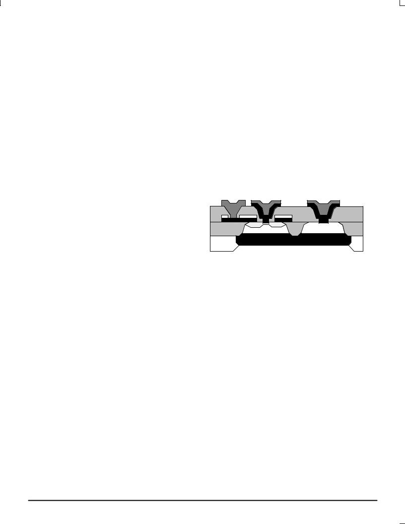
The MOSAIC III process is a double polysilicon process which uses a unique self-alignment scheme for device electrode and isolation definition. The process features self aligned submicron emitters as well as polysilicon base, collector and emitter electrodes. In addition, polysilicon resistors, diodes and capacitors are available to minimize the parasitic capacitance of an ECL gate. Figure 1.1 shows a cross section for an NPN device using the MOSAIC III process.
Figure 1.1. MOSAIC III Cross Section
By incorporating the use of polysilicon contacts and resistors through the MOSAIC III process, the parasitic capacitances of an ECLinPS gate are minimized, thus minimizing the time constants which comprise the switching delays of the gate. The resultant gates show delays of 100ps for internal gates and 200ps for output gates capable of driving 50Ω loads. The small geometries of the process, nearly 350% reduction in device area compared to a 10H device, allow these internal gate delays to be achieved at only 800μA of current.
Universal Compatibility
Each member of the ECLinPS family is available in both of the existing ECL standards: 10E series devices are compatible with the MECL 10H family; 100E series devices are compatible with ECL 100K. In addition, to maintain compatibility with temperature-compensated, three-level series-gated gate arrays, the 100E devices are guaranteed to operate without degradation to a VEE of ± 5.46V.
The section below presents a comparison between the two standards in the new context of the ECLinPS family. The user is also referred to the Electrical Characteristics section of this book as well as appropriate family data books and other literature for descriptive information on the earlier ECL families.
MOTOROLA |
1±2 |
ECLinPS and ECLinPS Lite |
|
|
DL140 Ð Rev 4 |

Because no supplier previous to Motorola has offered both ECL standards on an identical process, comparison of existing 10H and 100K style devices has some limitations. Comparison of the two standards fabricated with two different processes has sometimes led to the erroneous conclusion that there are inherent AC performance differences between them. In reality this is not the case. The only inherent difference between the two standards is the difference in the behavior of the DC characteristics with temperature.
AC Performance
From an IC design standpoint the only differences between a 10E device and a 100E device in the ECLinPS family is a small temperature compensation network in the 100E output gate, and very minimal differences in the two bias generator networks. Therefore one would expect that from an AC stand-point the performance of the two standards in the ECLinPS family should be nearly identical; measurements prove this to be the case. There is no significant measurable difference in the rise/fall times, propagation delays or toggle frequencies when comparing a 10E and 100E device. The minor difference between previous 10H and 100K designs is due to the fact that the two are fabricated on different processes, and in some cases are designed for operation at different power levels.
Summary
Summarizing the above information, in general, the two ECL design standards, although differing somewhat in DC parameters, are nearly identical when one compares the AC performance for a given device. There may be very small differences in the AC measurements due to the slightly smaller output swing of the 100E device. However, these differences are negligible when compared to the absolute value of the measurements. Therefore, from an AC stand-point, there is no real advantage in using one standard over the other, thus removing AC performance as a decision variable in high-speed system design.
Packaging
During the definition phase of the ECLinPS family, much attention was placed on the identification of a suitable package for the family. The package had to meet the criteria of minimum parasitics and propagation delays along with an attractive I/O vs board space relationship. Although the DIP package offered a level of familiarity and convenience, the performance of the package with a very high speed logic family was inadequate. In addition to the obvious parasitics and board space problems, the propagation delays through the DIP package were nearly twice as long as the delay through the silicon.
Family Overview
The 28-pin PLCC package emerged as the clear favorite both internally and with the high speed market in general. The package offers a quad layout to minimize both lead lengths and lead length differences. As a result, the parasitics and delays of the package are very well suited for a high speed logic family. In addition, the nearly matched lead lengths allow for tighter skew among similar paths through the chip.
The board density potential of the PLCC is also attractive in that it allows for a nearly 100% reduction in board space when compared to the DIP alternative. The package is approximately a half inch square with 50 mil spaced J-bend leads. More detailed measurements can be found in the package section of this data book. The J-bend leads provide a smaller footprint than a gull wing package and propose fewer temperature expansion coefficient mismatch problems than the leadless alternative.
Thermally, the standard PLCC exhibits a ΘJA of 43.5°C per watt at 500lfpm air flow. With this thermal resistance most
28-pin functions can be implemented with the MOSAIC III 1 process without encountering any severe thermal problems.
For more details on thermal issues of the ECLinPS family refer to the thermal section of this data book.
Abbreviation Definitions
The following is a list of abbreviations found in this data book and a brief definition of each.
Current
ICC |
Total power supply current drawn from the positive |
|
supply by an ECLinPS unit under test. |
IEE |
Total power supply current drawn from an ECLinPS |
|
device under test by the negative supply. |
IIL |
Current drawn by the input of an ECLinPS device with a |
|
specified low level (VIL min) forced on the input. |
IINH |
Current drawn by the input of an ECLinPS device with a |
|
specified high level (VIH max) forced on the input. |
IOUT |
The current sourced by an output under specified load |
|
conditions. |
Voltage |
|
VBB |
The switching reference voltage. |
VBE |
Base-to-emitter voltage drop of a transistor at specified |
|
collector and base currents. |
VCB |
Collector-to-base voltage drop of a transistor at |
|
specified collector and base currents. |
ECLinPS and ECLinPS Lite |
1±3 |
MOTOROLA |
DL140 Ð Rev 4

Family Overview
VCC |
The most positive supply voltage to an ECLinPS |
|
device. |
VCCO |
Power supply connection to the output emitter follower |
|
of an ECLinPS gate. For the ECLinPS logic family VCC |
|
and VCCO are common nodes. |
VEE |
The most negative supply voltage to an ECLinPS |
|
device. |
VIH |
Nominal input logic HIGH voltage level. |
VIH max |
Maximum (most positive) logic HIGH voltage level for |
|
which all parametric specifications hold. |
VIH min |
Minimum (least positive) logic HIGH voltage level for |
|
which all parametric specifications hold. |
1 VIL
VIL max
VIL min
VOH
VOHA
VOH max
VOH min
VOL
VOLA
VOL max
VOL min
VTT
VPP
VCMR
Nominal input logic LOW voltage.
Maximum (most positive) logic LOW voltage level for which all parametric specifications hold.
Minimum (least positive) logic HIGH voltage level for which all parametric specifications hold.
Output logic HIGH voltage level for the specified load condition.
Output logic HIGH voltage level with the inputs biased at VIH min or VOL max.
Maximum (most positive) logic HIGH output voltage level.
Minimum (least positive) logic HIGH output voltage level.
Output logic LOW voltage level for the specified load condition.
Output logic LOW voltage level with the inputs biased at VIH min or VOL max.
Maximum (most positive) logic LOW output voltage level.
Minimum (least positive) logic LOW output voltage level.
Output termination voltage for ECLinPS open emitter follower outputs.
Minimum peak-to-peak input voltage for differential input devices.
The voltage range in which the logic HIGH voltage level of a differential input signal must fall for a differential input device.
VCUT |
The logic LOW voltage level for ECL BUS outputs |
|
which attain cutoff of the output emitter follower. |
VSUP |
The maximum voltage difference between VEE and |
|
VCC for the E1651 comparator. |
Timing Parameters |
|
tR |
Waveform rise time of an output signal measured from |
|
the 20% to 80% levels of the signal. |
tF |
Waveform fall time of an output signal measured from |
|
the 20% to 80% levels of the signal. |
TPD±± |
Propagation delay of a signal measured for a |
|
rising/falling input to a rising/falling output. |
xpt |
The crossing point of a differential input or output |
|
signal. The reference point for which differential delays |
|
are measured. |
TPLH |
The propagation delay for an output transitioning from |
|
a logic LOW level to a logic HIGH level. |
TPHL |
The propagation delay for an output transitioning from |
|
a logic HIGH level to a logic LOW level. |
fMAX |
Maximum input frequency for which an ECLinPS flip |
|
flop will function correctly. |
fCOUNT |
Maximum input frequency for which an ECLinPS |
|
counter will function properly. |
fSHIFT |
Maximum input frequency for which an ECLinPS shift |
|
register will function properly. |
tSKEW |
The maximum delay difference between similar paths |
|
on a single ECLinPS device. |
ts |
Setup time: the minimum amount of time an input must |
|
transition before a clock transition to ensure proper |
|
function of the device. |
tH |
Hold time: the minimum amount of time an input must |
|
remain asserted after a clock transition to ensure |
|
proper operation of the device. |
tRR |
Release time or Reset Recovery Time: the minimum |
|
amount of time after a signal is de-asserted that a |
|
different input must wait before assertion to ensure |
|
proper functionality of the device. |
tw min |
Minimum pulse width of a signal necessary to ensure |
|
proper functionality of a device. |
MOTOROLA |
1±4 |
ECLinPS and ECLinPS Lite |
|
|
DL140 Ð Rev 4 |

Temperature
TSTG |
The maximum temperature at which a device may be |
|
stored without damage or performance degradation. |
TJ |
Junction (or die) temperature of an integrated circuit |
|
device. |
TA |
Ambient (environment) temperature existing in the |
|
immediate vicinity of an integrated circuit package. |
ΘJA |
Thermal resistance of an integrated circuit package |
|
between the junction and the ambient. |
ΘJC |
Thermal resistance of an integrated circuit package |
|
between the junction and the case. |
ΘCA |
Thermal resistance of an integrated circuit package |
|
between the case and the ambient. |
lfpm |
Linear feet per minute. |
|
Family Overview |
|
|
Miscellaneous |
|
||
DUT |
Device under test. |
|
|
CIN |
Input capacitance of a device. |
|
|
ZIN |
Input impedance of a device. |
|
|
COUT |
Output capacitance of a device. |
|
|
ZOUT |
Output impedance of a device. |
|
|
PD |
The total dc power applied to a device, not including |
|
|
|
any power delivered from the device to the load. |
|
|
RL |
Load resistance. |
|
|
RT |
|
|
|
Transmission line termination resistor. |
1 |
||
RP |
An input pull-down resistor. |
||
|
|||
PUT |
Pin under test. |
|
|
SMA |
Industry standard PCB connector. |
|
|
ECLinPS and ECLinPS Lite |
1±5 |
MOTOROLA |
DL140 Ð Rev 4 |
|
|