


SECTION 2
SPECIFICATIONS
INTRODUCTIONPRELIMINARY
The MC68181 is fabricated in high density CMOS with Transistor-Transistor Logic (TTL) compatible inputs and outputs.
MAXIMUM RATINGS
CAUTION
This device contains circuitry protecting against damage due to high static voltage or electrical fields; however, normal precautions should be taken to avoid exceeding maximum voltage ratings. Reliability is enhanced if unused inputs are tied to an appropriate logic voltage level (e.g., either GND or VCC).
Note: In the calculation of timing requirements, adding a maximum value of one specification to a minimum value of another specification does not yield a reasonable sum. A maximum specification is calculated using a worst case variation of process parameter values in one direction. The minimum specification is calculated using the worst case for the same parameters in the opposite direction. Therefore, a “maximum” value for a specification will never occur in the same device that has a “minimum” value for another specification; adding a maximum to a minimum represents a condition that can never exist.
MOTOROLA |
MC68181/D |
2-1 |

MC68181
Thermal characteristics
Table 2-1 Maximum Ratings
|
|
Rating1 |
|
Symbol |
|
Value1, 2 |
|
|
|
Unit |
|||
|
|
|
|
|
|
|
|
|
|
|
|
||
Supply Voltage |
|
VCC |
|
|
−0.3 to +3.6 |
|
|
|
V |
||||
All input voltages |
|
VIN |
|
GND − 0.5 to VCC + 0.5 |
|
V |
|||||||
Current drain per pin excluding VDD and VSS |
|
|
I |
|
|
10 |
|
|
|
mA |
|||
Operating temperature range |
|
TA |
|
|
–30 to +85 |
|
|
|
°C |
||||
Storage temperature |
|
TSTG |
|
|
–55 to +150 |
Y |
|
°C |
|||||
|
|
|
|
|
|
||||||||
Note: |
1. GND = 0 V, VCC = 1.8 to 3.3 V, TA = 0 C to +70 C |
|
|
|
|
|
|
|
|
||||
|
2. |
Absolute maximum ratings are stress°ratings |
only, and functional operation at the maximum is not |
||||||||||
|
|
° |
|
|
|
|
|
|
|
|
|
||
|
|
guaranteed. Stress beyond the maximum rating may affect device reliability or cause permanent |
|||||||||||
|
|
damage to the device. |
|
|
|
|
|
|
|
|
|
|
|
|
|
|
|
|
|
|
|
|
|
|
|
|
|
THERMAL CHARACTERISTICS |
|
|
|
A |
|
|
|
|
|||||
|
|
|
|
|
R |
|
|
||||||
|
|
Table 2-2 Thermal Characteristics |
|
|
|
|
|
|
|||||
|
|
|
|
|
|
|
|
|
|
||||
|
PRELIMI |
|
Symbol |
|
TQFP Value |
|
|
Unit |
|||||
|
|
Characteristic |
|
|
|
|
|
||||||
|
|
N |
|
|
|
|
|
||||||
Junction-to-ambient thermal resistance1 |
|
R JA or θJA |
|
95 |
|
|
°C/W |
||||||
|
|
|
|
|
|
θ |
|
|
|
|
|
|
|
Thermal characterization parameter |
|
|
|
ΨJT |
|
21 |
|
|
°C/W |
||||
Note: |
1. Junction-to-ambient thermal resistance is based on measurements on a horizontal, single-sided |
||||||||||||
Printed Circuit Board per SEMI G38-87 in natural convection.(SEMI is Semiconductor Equipment and Materials International, 805 East Middlefield Rd., Mountain View, CA 94043, (415) 964-5111) Values were measured with the parts mounted on thermal test boards meeting the specification EIA/ JESD51-3.
2-2 |
MC68181/D |
MOTOROLA |
MC68181
DC Electrical Characteristics
DC ELECTRICAL CHARACTERISTICS
Table 2-3 DC Electrical Characteristics
|
|
|
Characteristics |
|
|
Symbol |
Min |
Typ |
Max |
|
Unit |
|||||
|
|
|
|
|
|
|
|
|
|
|
||||||
|
|
|
|
|
|
|
|
|
|
|
||||||
Supply voltage |
|
|
|
VCC |
|
1.8 |
2.0 or 3.3 |
3.6 |
|
V |
||||||
Input high voltage |
|
|
|
VIH |
|
|
|
|
|
|
|
|||||
|
|
|
|
PRELIMINARY |
VCC |
|
V |
|||||||||
|
RESET, SS, SCK, MOSI |
|
|
|
|
0.75 VDD |
— |
|
||||||||
|
All other inputs |
|
|
|
|
0.7 |
× |
— |
VCC |
|
V |
|||||
|
|
|
|
|
×VDD |
|
||||||||||
Input low voltage |
|
|
|
VIL |
|
— |
— |
0.2 × VDD |
|
V |
||||||
Input leakage current |
|
|
IIN |
–0.25 |
— |
0.25 |
|
μA |
||||||||
High impedance (off-state) input current |
I |
TSI |
|
–10 |
— |
+10 |
|
μ |
A |
|||||||
(@ 1.44 V /0.3 V) |
|
|
|
|
|
|
|
|
|
|
||||||
Output high voltage (IOH = –1.0 mA) |
VOH |
0.8 × VDD |
— |
— |
|
V |
||||||||||
Output low voltage (IOL = 2.8 mA) |
VOL |
|
— |
— |
0.3 |
|
V |
|||||||||
Internal Supply Current1 |
|
|
ICC |
|
— |
100 |
— |
|
μA |
|||||||
Input capacitance |
|
|
|
CIN |
|
— |
10 |
— |
|
pF |
||||||
Note: 1. This value is for static ICC. |
|
|
|
|
|
|
|
|
|
|||||||
|
|
|
|
|
|
|
|
|
||||||||
AC ELECTRICAL CHARACTERISTICS |
|
|
|
|
|
|
||||||||||
|
|
The timing waveforms in the AC Electrical Characteristics are tested with a VIL |
|
|
||||||||||||
|
|
maximum of 0.2 |
|
VDD in V and a VIH minimum of 0.7 VDD in V for all inputs. AC |
||||||||||||
|
|
timing |
specifications that are referenced to a device input signal are measured in |
|
||||||||||||
|
|
|
× |
|
|
|
|
|
× |
|
|
|
|
|||
production with respect to the 50% point of the respective input signal’s transition. MC68181 output levels are measured with the production test machine VOL and VOH reference levels set at 0.3 × VDD in V and 0.6 × VDD in V, respectively.
MOTOROLA |
MC68181/D |
2-3 |
MC68181
Initialization Timing
INITIALIZATION TIMING
(VCC = 1.8 to 3.6 V, TA = –30 to + 85°C)
Table 2-4 Initialization Timing
Characteristic |
Conditions Symbol |
Min |
Max |
Unit |
|
Oscillator Start-up Time |
— |
tSTART |
— |
5 |
sec |
|||||
|
|
Hold Time |
— |
tRESET |
200 |
— |
ns |
||||
|
RESET |
||||||||||
|
|
High to |
|
Low |
— |
tRHRL |
76,800 |
76,800 |
T |
||
|
RESET |
READY |
|||||||||
|
|
|
|
|
|
|
|
|
|
Y |
|
|
|
|
|
|
|
|
|
|
|
|
|
|
Oscillator Warmed Up to READY Low |
CL = 50pf |
tOWRL |
— |
1 |
sec |
|||||
Note: T is one period of the 76.8 kHz clock source. From power-up, the oscillator start-up time can impact the availability |
||||||||||||||||||||||||||||||||||||||||||
|
and period of clock strobes. This can affect the actual |
|
high to |
|
|
low timing.R |
|
|
|
|
|
|||||||||||||||||||||||||||||||
RESET |
READY |
|
|
|
|
|
||||||||||||||||||||||||||||||||||||
|
|
|
|
|
|
|
|
|
|
|
|
|
|
|
|
|
|
|
|
|
|
|
|
|
|
|
|
|
|
|
|
|
A |
|
|
|
|
|
||||
|
VDD |
|
|
|
|
|
|
|
|
|
N |
|
|
|
|
|
|
|
|
|
|
|||||||||||||||||||||
|
|
|
|
|
|
|
|
|
|
|
|
|
|
|
|
|
|
|
|
|
|
|
|
|
|
|
|
|
|
|
|
|
|
|
|
|||||||
Oscillator |
|
|
|
|
|
tSTART |
|
|
|
|
|
|
|
|
|
|
|
|
|
|
|
|
|
|
|
|
|
|
|
|||||||||||||
|
|
|
|
|
|
|
|
|
|
|
|
|
|
|
|
|
|
|
|
|
|
|
||||||||||||||||||||
|
|
|
|
|
|
|
|
|
|
|
|
|
|
|
|
|
|
|
|
|
|
|
|
|
|
|
|
|
|
|||||||||||||
|
|
|
|
|
|
|
|
|
|
|
|
|
|
|
|
|
|
|
|
|
|
|
|
|
|
|
|
|
|
|
|
|||||||||||
|
|
|
|
|
|
|
|
|
|
|
|
|
|
|
|
|
|
|
|
|
|
|
|
|
|
|
|
|||||||||||||||
|
|
|
|
|
|
|
|
|
|
|
|
|
|
|
|
|
|
|
|
|
|
|
|
|
|
|
|
|
|
|
|
|
|
|
|
|
|
|
||||
|
|
|
|
|
|
|
|
|
|
|
|
|
|
|
|
|
|
|
|
|
|
|
|
|
|
|
|
|
|
|
|
|
|
|
|
|
|
|
|
|
|
|
|
|
|
|
|
|
|
|
|
|
|
|
|
|
|
|
|
|
|
|
|
|
|
|
|
|
|
|
|
|
|
|
|
|
|
|
|
|
|
|
|
|
|
|
|
|
|
|
|
|
|
|
|
|
|
|
|
|
|
|
|
|
|
|
|
|
|
|
|
|
|
|
|
|
|
|
|
|
|
|
|
|
||||
|
RESET |
|
|
|
|
|
|
|
|
|
|
|
|
|
|
|
|
|
|
|
||||||||||||||||||||||
|
|
|
|
|
|
|
|
|
|
|
|
|
|
|
|
|
|
|
|
|
|
|
|
|
|
|
|
|
|
|
|
|
|
|||||||||
|
|
|
|
|
|
|
|
|
|
|
|
|
|
|
|
|
|
|
|
|
|
|
|
|
|
|
|
|
|
|
|
|
|
|||||||||
|
|
|
|
|
|
|
|
|
|
tRESET |
|
|
|
|
|
|
|
|
|
|
|
|
|
|
|
|
|
|
|
|
|
|
|
|
|
|
|
|||||
|
|
|
|
|
|
|
|
|
|
|
|
|
|
|
|
|
|
|
|
|
|
|
|
|
|
|
|
|
|
|
|
|
|
|
|
|
|
|
|
|
|
|
|
READY |
|
|
|
|
|
|
|
|
|
|
|
|
|
|
|
|
|
|
|
|
|
|
|
|
|
|
|
|
|
|
|
|
|
|
|
|
|||||
|
|
|
|
|
|
|
|
|
|
|
|
|
|
|
|
|
|
|
|
|
|
|
|
|
|
|
|
|
|
|
|
|
|
|
|
|
|
|
|
|
|
|
|
|
|
|
|
|
|
|
|
|
|
|
|
|
|
|
|
|
|
|
|
|
|
|
|
|
|
|
|
|
|
|
|
|
|
|
|
|
|
|
|
|
|
|
|
|
|
|
|
|
|
|
|
|
|
|
|
|
|
|
|
|
|
|
|
|
|
|
|
|
|
|
|
|
|
|
|
|
|
|
|
|
|
|
|
|
|
|
|
|
|
|
|
|
|
|
|
|
|
|
|
|
|
|
|
|
|
|
|
|
|
|
|
|
|
|
|
|
|
|
|
|
|
|
|
|
|
|
|
|
|
|
|
|
|
|
|
|
|
|
|
|
|
|
|
|
|
|
|
|
|
|
|
|
|
|
|
|
|
|
|
tOWRL |
|
|
|
|
|
|||||
|
|
|
|
|
|
|
|
|
|
|
|
|
|
|
|
|
|
|
|
|
|
|
|
|
|
|
|
|
|
|
|
|
|
|
|
|
|
|
|
|||
|
|
|
|
|
|
|
|
|
|
|
|
|
|
|
|
|
|
|
|
|
|
|
|
|
|
|
|
|
|
tRHRL |
|
|
|
|
|
|
AA122 |
|||||
|
|
|
|
|
|
|
|
|
|
|
|
|
|
|
|
|
|
|
|
|
|
|
|
|
|
|
|
|
|
|
|
|
||||||||||
|
|
|
|
|
|
|
|
|
|
|
|
|
|
|
|
|
|
|
|
|
|
|
|
|
|
|
|
|
|
|
|
|
|
|
|
|||||||
|
|
|
|
|
|
|
|
|
|
|
|
|
|
|
|
|
|
|
|
|
|
|
|
|
|
|
|
|
|
|
|
|
|
|
|
|
|
|
|
|||
|
|
|
|
|
|
|
|
|
|
|
|
|
|
|
Figure 2-1 |
Startup Timing |
|
|
|
|
|
|
|
|
|
|
||||||||||||||||
|
PRELIMI |
|
|
|
|
|
|
|
|
|
|
|
|
|
|
|
||||||||||||||||||||||||||
2-4 |
MC68181/D |
MOTOROLA |

MC68181
RESET Timing
RESET TIMING
(VCC = 1.8 to 3.6 V, TA = –30 to 85°C)
Table 2-5 Reset Timing
Characteristic |
Conditions |
Symbol |
Min |
Max |
Unit |
|
|
|
PRELIMINARY |
|
|
|||||||||||||||||||||||||||||||||
|
RESET Pulse Width |
— |
tRL |
200 |
— |
ns |
||||||||||||||||||||||||||||||||
|
|
|
Low to |
|
|
|
|
|
|
|
|
|
|
|
High |
— |
tRLRH |
— |
200 |
|
|
ns |
||||||||||||||||
|
RESET |
READY |
||||||||||||||||||||||||||||||||||||
|
|
|
High to |
|
|
|
|
|
|
|
|
|
|
|
Low |
Requires stable |
tRHRL |
— |
1 |
|
|
|
sec |
|||||||||||||||
|
RESET |
READY |
||||||||||||||||||||||||||||||||||||
|
|
|
|
|
|
|
|
|
|
|
|
|
|
|
|
|
|
|
|
|
|
|
|
|
|
|
|
|
|
76.8 kHz clock source |
|
|
|
|
|
|
|
|
|
|
|
|
|
|
|
|
|
|
|
|
|
|
|
|
|
|
|
|
|
|
|
|
|
|
|
|
|
|
|
|
|
|
|||||
|
|
|
|
|
|
|
|
|
|
|
|
|
|
|
|
|
|
|
|
|
|
|
|
|
|
|
|
|
|
|
|
|
|
|||||
|
|
|
|
|
|
|
|
|
|
|
|
|
|
|
|
|
|
|
|
|
|
|
|
|
|
|
|
|
|
|
|
|
|
|
||||
|
|
RESET |
|
|
|
|
|
|
|
|
|
|||||||||||||||||||||||||||
|
|
|
|
|
|
|
|
|
|
|
|
|
|
|
|
|
|
|
|
|
|
|
|
|
|
|
|
|
|
|
|
|
|
|
|
|
||
|
|
|
|
|
|
|
|
|
|
|
|
|
|
|
|
|
|
|
|
|
|
|
|
|
|
|
|
|
|
|
|
|
|
|
|
|
||
|
|
|
|
|
|
|
|
|
|
|
|
|
|
|
|
|
|
|
|
|
|
|
|
|
|
|
|
|
|
|
|
|
|
|
|
|
||
|
|
|
|
|
|
|
|
|
|
|
|
|
|
|
|
|
|
|
|
|
|
|
|
|
|
|
|
|
|
|
|
|
|
|
|
|||
|
|
|
|
|
|
|
|
|
|
|
|
|
|
|
|
|
|
|
tRL |
|
|
|
|
|
|
|
|
|
|
|
|
|
|
|
|
|||
|
|
|
|
|
|
|
|
|
|
|
|
|
|
|
|
|
|
|
|
|
|
|
|
|
|
|
|
|
|
|||||||||
|
|
|
|
|
|
|
|
|
|
|
|
|
|
|
|
|
|
|
|
|
|
|
|
|
|
|
|
|
|
|
|
|
|
|
|
|
|
|
|
|
|
|
|
|
|
|
|
|
|
|
|
|
|
|
|
|
|
|
|
|
|
|
|
|
|
|
|
|
|
|
|
|
|
||||
|
READY |
|
|
|
|
|
|
|
|
|
||||||||||||||||||||||||||||
|
|
|
tRLRH |
|
|
|
|
|
|
|
|
|
|
tRHRL |
|
|
|
|
|
|
|
|
||||||||||||||||
|
|
|
|
|
|
|
|
|
|
|
|
|
|
|||||||||||||||||||||||||
|
|
|
|
|
|
|
|
|
|
|
|
|
|
|
|
|
|
|
|
|
|
|
|
|
|
|
|
|
|
|
|
|
|
|
|
|
|
|
AA122
Figure 2-2 Reset Timing
MOTOROLA |
MC68181/D |
2-5 |

MC68181
Serial Peripheral Interface (SPI) Timing
SERIAL PERIPHERAL INTERFACE (SPI) TIMING
(VCC = 1.8 to 3.6 V, TA = –30 to +85°C)
Table 2-6 SPI Timing
|
|
Characteristic |
Conditions |
|
Symbol |
Min |
|
Max |
Unit |
||
|
|
|
|
|
|
|
|
|
|||
|
|
|
|
|
|
|
|
|
|||
|
Operating Frequency |
— |
|
fOP |
0 |
|
1 |
MHz |
|||
|
Cycle Time |
— |
|
tCYC |
1000 |
|
— |
ns |
|||
|
Select Lead Time |
— |
|
tLEAD1 |
200 |
|
— |
ns |
|||
|
De-select Lag Time |
— |
|
tLAG1 |
200 |
|
— |
ns |
|||
|
|
|
|
|
|
|
|
Y |
|
|
|
|
Select-to-Ready Time |
Previous packet did not program an |
t |
RDY |
— |
|
80 |
μs |
|||
|
address word; CL = 50 pf |
|
|
|
|||||||
|
|
|
Previous packet programmed an |
|
t |
|
— |
|
420 |
μ |
s |
|
Select-to-Ready Time |
address word; CL = 50 pf |
|
|
RDY |
R |
|
|
|||
|
Ready High Time |
— |
|
tRHA |
50 |
|
— |
μs |
|||
|
Ready Lead Time |
— |
|
tLEAD2 |
|
|
|
||||
|
|
200 |
|
— |
ns |
||||||
|
Not Ready Lag Time |
CL = 50pf |
|
tLAG2 |
— |
|
200 |
ns |
|||
|
MOSI Data Setup Time |
— |
|
|
t |
200 |
|
— |
ns |
||
|
|
|
|
NSU |
|
|
|
|
|
||
|
MOSI Data Hold Time |
— |
|
|
tHI |
200 |
|
— |
ns |
||
|
MISO Access Time |
CL = 50pf |
|
tAC |
0 |
|
200 |
ns |
|||
|
MISO Disable Time |
— |
|
tDIS |
— |
|
300 |
ns |
|||
|
MISO Data Valid Time |
CL = 50pf |
|
|
tV |
— |
|
200 |
ns |
||
|
MISO Data Hold Time |
— |
|
tHO |
0 |
|
— |
ns |
|||
|
|
High Time |
— |
|
tSSH |
200 |
|
— |
ns |
||
|
SS |
|
|
||||||||
|
SCK High Time |
— |
|
tSCKH |
300 |
|
— |
ns |
|||
|
SCK Low Time |
— |
|
tSCKL |
300 |
|
— |
ns |
|||
|
SCK Rise Time |
20% to 70% VDD |
|
|
tR |
|
|
1 |
μs |
||
|
SCK Fall Time |
20% to 70% VDD |
|
|
tF |
|
|
1 |
μs |
||
Note: PRELIMIWhen the host reprograms an address word with a Host-to-FLEX™ chip packet ID > 127 (decimal), there may be an added delay before FLEX™ chip is ready for another packet.
2-6 |
MC68181/D |
MOTOROLA |

MC68181
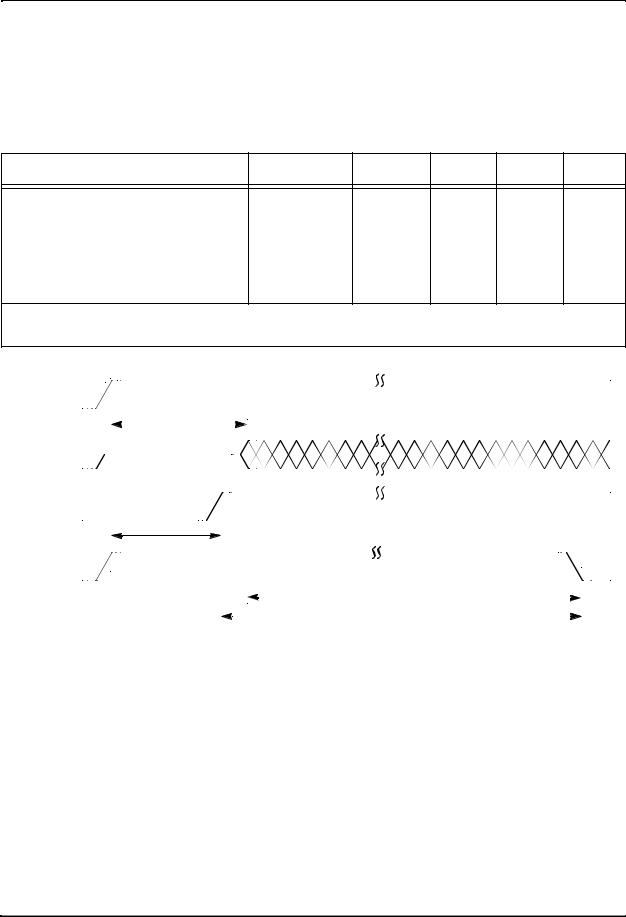
Serial Peripheral Interface (SPI) Timing
SS |
|
|
|
|
|
|
|
tSSH |
|
READY |
|
|
|
|
tRDY |
tCYC |
tLAG2 |
|
tRH |
tLEAD1 |
tLEAD2 |
tF |
tLAG1 |
|
tR |
||||
SCK |
|
|
|
|
tSCKL |
tSCKH |
|
Tri- |
|
Tri- |
|
|
|
|
stated |
D31 |
|
D0 |
stated |
MISO |
|
|
||
tAC |
tV |
tHO |
tDIS |
|
MOSI |
D31 |
|
D0 |
|
tSU |
tHI |
|
|
AA122 |
|
|
|
||
|
|
|
|
|
|
Figure 2-3 |
SPI Timing |
|
|
PRELIMINARY |
|
|||
MOTOROLA |
MC68181/D |
|
2-7 |
|

MC68181
Serial Peripheral Interface (SPI) Timing
|
Y |
|
R |
N |
A |
|
|
PRELIMI |
|
2-8 |
MC68181/D |
MOTOROLA |