

motorola / 4HCT373A
.PDFMOTOROLA
SEMICONDUCTOR TECHNICAL DATA
Octal 3-State Noninverting Transparent Latch with LSTTL-Compatible Inputs
High±Performance Silicon±Gate CMOS
The MC54/74HCT373A may be used as a level converter for interfacing TTL or NMOS outputs to High±Speed CMOS inputs.
The HCT373A is identical in pinout to the LS373.
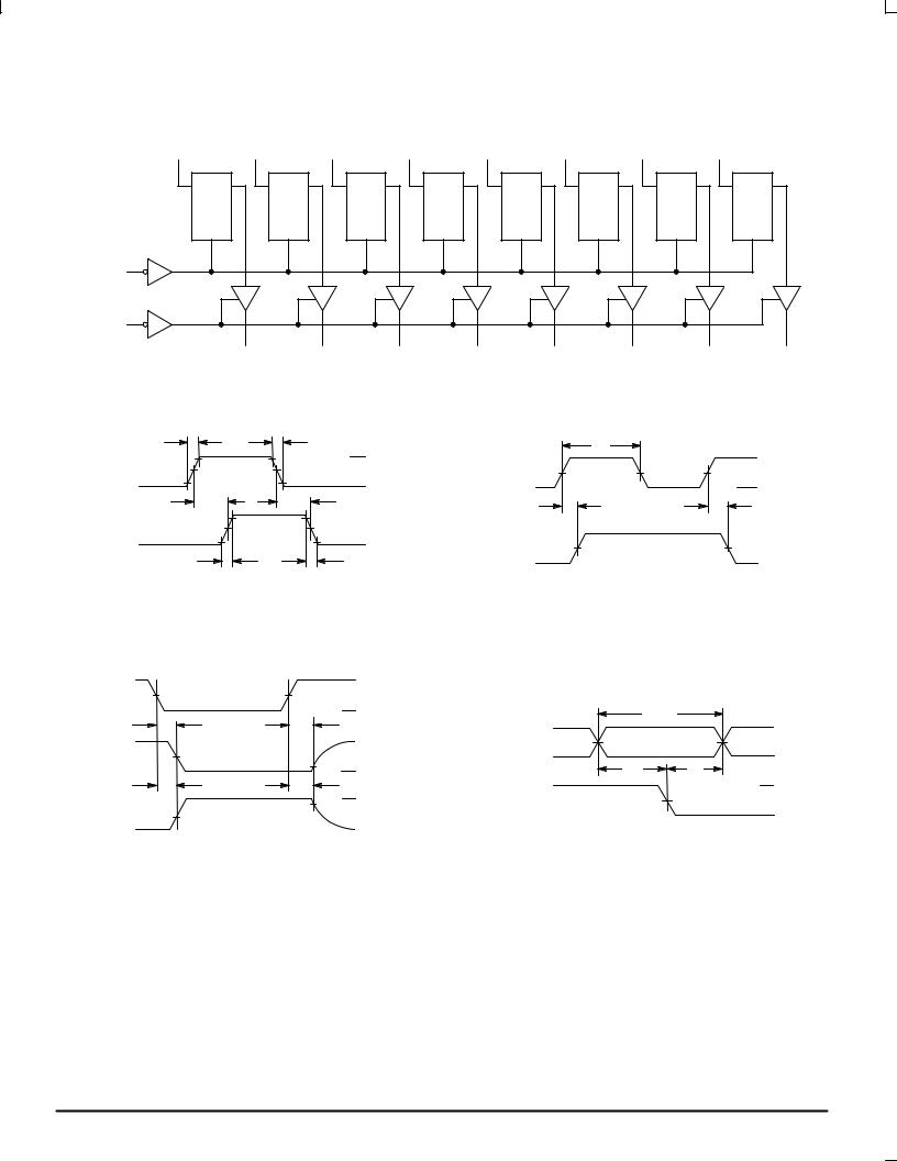
The eight latches of the HCT373A are transparent D±type latches. While the Latch Enable is high the Q outputs follow the Data Inputs. When Latch Enable is taken low, data meeting the setup and hold times becomes latched.
The Output Enable does not affect the state of the latch, but when Output Enable is high, all outputs are forced to the high±impedance state. Thus, data may be latched even when the outputs are not enabled.
The HCT373A is identical in function to the HCT573A, which has the input pins on the opposite side of the package from the output pins. This device is similar in function to the HCT533A, which has inverting outputs.
•Output Drive Capability: 15 LSTTL Loads
•TTL/NMOS±Compatible Input Levels
•Outputs Directly Interface to CMOS, NMOS, and TTL
•Operating Voltage Range: 4.5 to 5.5 V
•Low Input Current: 1.0 μA
•In Compliance with the Requirements Defined by JEDEC Standard No. 7A
•Chip Complexity: 196 FETs or 49 Equivalent Gates
LOGIC DIAGRAM
|
|
|
D0 |
3 |
|
|
|
|
2 |
Q0 |
|
|
|
|
|
|
4 |
|
|
|
|
5 |
|
|
|
||||
|
|
|
D1 |
|
|
|
|
Q1 |
|
|
|
|
||
|
|
7 |
|
|
|
|
6 |
|
|
|
||||
|
|
|
D2 |
|
|
|
|
Q2 |
|
|
|
|
||
|
DATA |
8 |
|
|
|
|
9 |
|
|
|
||||
|
|
|
|
|
|
|
|
|
|
|
|
|||
|
D3 |
|
|
|
|
Q3 |
NONINVERTING |
|||||||
|
|
|
|
|
|
|||||||||
|
INPUTS |
|
|
13 |
|
|
|
|
12 |
|
|
|||
|
|
D4 |
|
|
|
|
Q4 |
|
OUTPUTS |
|||||
|
|
|
|
|
|
|
|
|||||||
|
|
|
14 |
|
|
|
|
15 |
|
|
|
|||
|
|
|
D5 |
|
|
|
|
Q5 |
|
|
|
|
||
|
|
17 |
|
|
|
|
16 |
|
|
|
||||
|
|
|
D6 |
|
|
|
|
Q6 |
|
|
|
|
||
|
|
18 |
|
|
|
|
19 |
|
|
|
||||
|
|
|
D7 |
|
|
|
|
|
|
|
|
|
||
|
|
|
|
|
|
|
Q7 |
|
|
|
||||
|
|
|
|
|
|
|
|
|
|
|
||||
|
LATCH ENABLE |
11 |
|
|
|
|
|
PIN 20 = VCC |
||||||
|
|
|
|
|
|
|||||||||
|
1 |
|
|
|
|
|
PIN 10 = GND |
|||||||
OUTPUT ENABLE |
|
|
|
|
|
|||||||||
|
|
|
|
|
|
|
|
|
|
|||||
|
|
|
|
|
|
|
|
|
|
|
||||
|
|
|
|
|
|
|
|
|
||||||
|
|
|
Design Criteria |
|
Value |
|
Units |
|
||||||
|
|
|
|
|
|
|
|
|||||||
|
Internal Gate Count* |
|
49 |
|
|
ea. |
|
|||||||
|
|
|
|
|
|
|
|
|||||||
|
Internal Gate Propagation Delay |
|
1.5 |
|
|
ns |
|
|||||||
|
|
|
|
|
|
|
|
|||||||
|
Internal Gate Power Dissipation |
|
5.0 |
|
|
μW |
|
|||||||
|
|
|
|
|
|
|
||||||||
|
Speed Power Product |
|
.0075 |
|
pJ |
|
||||||||
|
|
|
|
|
|
|
|
|||||||
|
* Equivalent to a two±input NAND gate. |
|
|
|
|
|
|
|||||||
MC54/74HCT373A
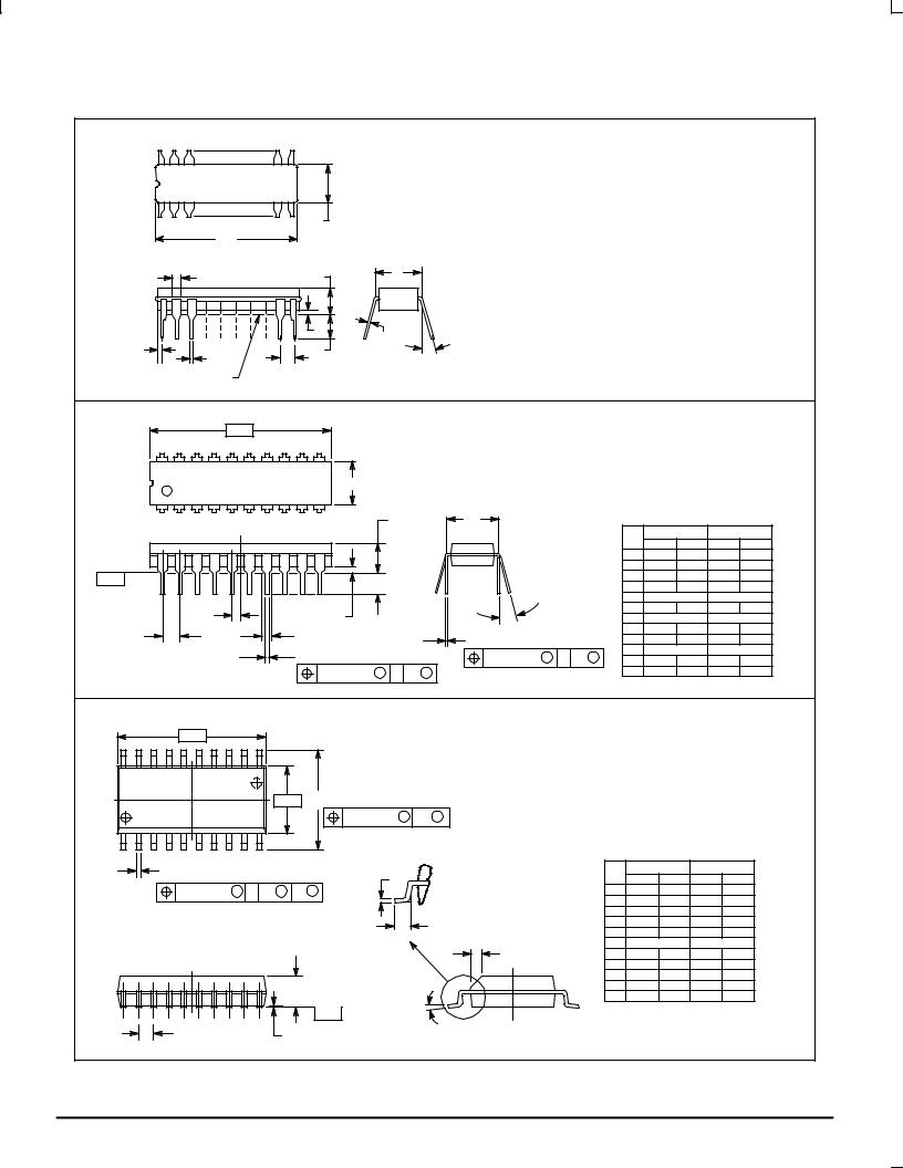
|
J SUFFIX |
|
20 |
CERAMIC PACKAGE |
|
CASE 732±03 |
||
|
||
|
1 |
|
|
N SUFFIX |
|
20 |
PLASTIC PACKAGE |
|
CASE 738±03 |
||
|
||
|
1 |
DW SUFFIX
20 |
SOIC PACKAGE |
1 |
CASE 751D±04 |
|
20 |
SD SUFFIX |
|
SSOP PACKAGE |
||
1 |
CASE 940C±03 |
|
20 |
DT SUFFIX |
|
TSSOP PACKAGE |
||
1 |
||
CASE 948E±02 |
ORDERING INFORMATION
MC54HCTXXXAJ Ceramic
MC74HCTXXXAN Plastic
MC74HCTXXXADW SOIC
MC74HCTXXXASD SSOP
MC74HCTXXXADT TSSOP
PIN ASSIGNMENT
OUTPUT |
|
1 |
20 |
VCC |
|
|
|||||
|
|
||||
ENABLE |
|||||
|
|
|
|||
Q0 |
|
2 |
19 |
Q7 |
|
D0 |
|
3 |
18 |
D7 |
|
|
|||||
D1 |
|
4 |
17 |
D6 |
|
|
|||||
Q1 |
|
5 |
16 |
Q6 |
|
|
|||||
Q2 |
|
6 |
15 |
Q5 |
|
|
|||||
D2 |
|
7 |
14 |
D5 |
|
|
|||||
D3 |
|
8 |
13 |
D4 |
|
|
|||||
Q3 |
|
9 |
12 |
Q4 |
|
|
|||||
GND |
|
10 |
11 |
LATCH |
|
|
|||||
|
|
|
|
ENABLE |
|
|
|
|
|
||
FUNCTION TABLE
|
Inputs |
|
Output |
|
|
|
|
Output |
Latch |
|
|
Enable |
Enable |
D |
Q |
|
|
|
|
L |
H |
H |
H |
L |
H |
L |
L |
L |
L |
X |
No Change |
H |
X |
X |
Z |
|
|
|
|
X = don't care
Z = high impedance
10/95
Motorola, Inc. 1995 |
REV 6 |
MC54/74HCT373A
MAXIMUM RATINGS*
Symbol |
Parameter |
Value |
Unit |
|
|
|
|
|
|
VCC |
DC Supply Voltage (Referenced to GND) |
± 0.5 to + 7.0 |
V |
|
Vin |
DC Input Voltage (Referenced to GND) |
± 1.5 to VCC + 1.5 |
V |
|
Vout |
DC Output Voltage (Referenced to GND) |
± 0.5 to VCC + 0.5 |
V |
|
Iin |
DC Input Current, per Pin |
± 20 |
mA |
|
Iout |
DC Output Current, per Pin |
± 35 |
mA |
|
ICC |
DC Supply Current, VCC and GND Pins |
± 75 |
mA |
|
PD |
Power Dissipation in Still Air, Plastic or Ceramic DIP² |
750 |
mW |
|
|
SOIC Package² |
500 |
|
|
|
SSOP or TSSOP Package² |
450 |
|
|
|
|
|
|
|
Tstg |
Storage Temperature |
± 65 to + 150 |
_C |
|
TL |
Lead Temperature, 1 mm from Case for 10 Seconds |
|
_C |
|
|
(Plastic DIP, SOIC, SSOP or TSSOP Package) |
260 |
|
|
|
(Ceramic DIP) |
300 |
|
|
|
|
|
|
This device contains protection circuitry to guard against damage due to high static voltages or electric fields. However, precautions must be taken to avoid applications of any voltage higher than maximum rated voltages to this high±impedance circuit. For proper operation, Vin and
Vout should be constrained to the
range GND v (Vin or Vout) v VCC. Unused inputs must always be
tied to an appropriate logic voltage level (e.g., either GND or VCC). Unused outputs must be left open.
*Maximum Ratings are those values beyond which damage to the device may occur. Functional operation should be restricted to the Recommended Operating Conditions.
²Derating Ð Plastic DIP: ± 10 mW/ _C from 65_ to 125_C Ceramic DIP: ± 10 mW/_C from 100_ to 125_C
SOIC Package: ± 7 mW/_C from 65_ to 125_C
SSOP or TSSOP Package: ± 6.1 mW/_C from 65_ to 125_C
For high frequency or heavy load considerations, see Chapter 2 of the Motorola High±Speed CMOS Data Book (DL129/D).
RECOMMENDED OPERATING CONDITIONS
Symbol |
Parameter |
Min |
Max |
Unit |
|
|
|
|
|
VCC |
DC Supply Voltage (Referenced to GND) |
4.5 |
5.5 |
V |
Vin, Vout |
DC Input Voltage, Output Voltage (Referenced to GND) |
0 |
VCC |
V |
TA |
Operating Temperature, All Package Types |
± 55 |
+ 125 |
_C |
tr, tf |
Input Rise and Fall Time (Figure 1) |
0 |
500 |
ns |
DC ELECTRICAL CHARACTERISTICS (Voltages Referenced to GND)
|
|
|
|
Guaranteed Limit |
|
||
|
|
|
VCC |
|
|
|
|
|
|
|
± 55 to |
|
|
|
|
Symbol |
Parameter |
Test Conditions |
V |
25_C |
v 85_C |
v 125_C |
Unit |
|
|
|
|
|
|
|
|
VIH |
Minimum High±Level Input |
Vout = 0.1 V or VCC ± 0.1 V |
4.5 |
2.0 |
2.0 |
2.0 |
V |
|
Voltage |
|Iout| v 20 μA |
5.5 |
2.0 |
2.0 |
2.0 |
|
VIL |
Maximum Low±Level Input |
Vout = 0.1 V or VCC ± 0.1 V |
4.5 |
0.8 |
0.8 |
0.8 |
V |
|
Voltage |
|Iout| v 20 μA |
5.5 |
0.8 |
0.8 |
0.8 |
|
VOH |
Minimum High±Level Output |
Vin = VIH or VIL |
4.5 |
4.4 |
4.4 |
4.4 |
V |
|
Voltage |
|Iout| v 20 μA |
5.5 |
5.4 |
5.4 |
5.4 |
|
|
|
Vin = VIH or VIL |
|
|
|
|
|
|
|
|Iout| v 6.0 mA |
4.5 |
3.98 |
3.84 |
3.7 |
|
VOL |
Maximum Low±Level Output |
Vin = VIH or VIL |
4.5 |
0.1 |
0.1 |
0.1 |
V |
|
Voltage |
|Iout| v 20 μA |
5.5 |
0.1 |
0.1 |
0.1 |
|
|
|
Vin = VIH or VIL |
|
|
|
|
|
|
|
|Iout| v 6.0 mA |
4.5 |
0.26 |
0.33 |
0.4 |
|
Iin |
Maximum Input Leakage Current |
Vin = VCC or GND |
5.5 |
± 0.1 |
± 1.0 |
± 1.0 |
μA |
MOTOROLA |
2 |
MC54/74HCT373A
DC ELECTRICAL CHARACTERISTICS (Voltages Referenced to GND)
|
|
|
|
Guaranteed Limit |
|
||||
|
|
|
|
|
|
|
|
|
|
|
|
|
VCC |
± 55 to |
|
|
|
|
|
Symbol |
Parameter |
Test Conditions |
V |
25_C |
|
v 85_C |
v 125_C |
Unit |
|
|
|
|
|
|
|
|
|
|
|
IOZ |
Maximum Three±State |
Output in High±Impedance State |
5.5 |
± 0.5 |
|
± 5.0 |
± 10 |
μA |
|
|
Leakage Current |
Vin = VIL or VIH |
|
|
|
|
|
|
|
|
|
Vout = VCC or GND |
|
|
|
|
|
|
|
ICC |
Maximum Quiescent Supply |
Vin = VCC or GND |
5.5 |
4.0 |
|
40 |
160 |
μA |
|
|
Current (per Package) |
Iout = 0 μA |
|
|
|
|
|
|
|
|
|
|
|
|
|
|
|
||
ICC |
Additional Quiescent Supply |
Vin = 2.4 V, Any One Input |
5.5 |
≥ ±55_C |
|
25_C to 125_C |
mA |
||
|
Current |
Vin = VCC or GND, Other Inputs |
|
|
|
|
|
|
|
|
|
2.9 |
|
|
|
2.4 |
|
||
|
|
lout = 0 μA |
|
|
|
|
|
||
|
|
|
|
|
|
|
|
|
|
NOTE: 1. Total Supply Current = ICC + ΣΔICC.
NOTE: Information on typical parametric values can be found in Chapter 2 of the Motorola High±Speed CMOS Data Book (DL129/D).
AC ELECTRICAL CHARACTERISTICS (VCC = 5.0 V ± 10%, CL = 50 pF, Input tr = tf = 6.0 ns)
|
|
|
Guaranteed Limit |
|
||
|
|
|
|
|
|
|
|
|
± 55 to |
|
|
|
|
Symbol |
Parameter |
25_C |
|
v 85_C |
v 125_C |
Unit |
|
|
|
|
|
|
|
tPLH, |
Maximum Propagation Delay, Input D to Q |
28 |
|
35 |
42 |
ns |
tPHL |
(Figures 1 and 5) |
|
|
|
|
|
tPLH, |
Maximum Propagation Delay, Latch Enable to Q |
32 |
|
40 |
48 |
ns |
tPHL |
(Figures 2 and 5) |
|
|
|
|
|
tPLZ, |
Maximum Propagation Delay, Output Enable to Q |
30 |
|
38 |
45 |
ns |
tPHZ |
(Figures 3 and 6) |
|
|
|
|
|
tPZL, |
Maximum Propagation Delay, Output Enable to Q |
35 |
|
44 |
53 |
ns |
tPZH |
(Figures 3 and 6) |
|
|
|
|
|
tTLH, |
Maximum Output Transition Time, Any Output |
12 |
|
15 |
18 |
ns |
tTHL |
(Figures 1 and 5) |
|
|
|
|
|
Cin |
Maximum Input Capacitance |
10 |
|
10 |
10 |
pF |
Cout |
Maximum Three±State Output Capacitance |
15 |
|
15 |
15 |
pF |
|
(Output in High±Impedance State) |
|
|
|
|
|
|
|
|
|
|
|
|
NOTE: For propagation delays with loads other than 50 pF, and information on typical parametric values, see Chapter 2 of the Motorola High± Speed CMOS Data Book (DL129/D).
|
|
Typical @ 25°C, VCC = 5.0 V |
|
CPD |
Power Dissipation Capacitance (Per Latch)* |
65 |
pF |
*Used to determine the no±load dynamic power consumption: PD = CPD VCC2f + ICC VCC. For load considerations, see Chapter 2 of the Motorola High±Speed CMOS Data Book (DL129/D).
TIMING REQUIREMENTS (VCC = 5.0 V ± 10%, Input tr = tf = 6.0 ns)
|
|
|
Guaranteed Limit |
|
||
|
|
|
|
|
|
|
|
|
± 55 to |
|
|
|
|
Symbol |
Parameter |
25_C |
|
v 85_C |
v 125_C |
Unit |
|
|
|
|
|
|
|
tsu |
Minimum Setup Time, Input D to Latch Enable |
10 |
|
13 |
15 |
ns |
|
(Figure 4) |
|
|
|
|
|
|
|
|
|
|
|
|
th |
Minimum Hold Time, Latch Enable to Input D |
10 |
|
13 |
15 |
ns |
|
(Figure 4) |
|
|
|
|
|
|
|
|
|
|
|
|
tw |
Minimum Pulse Width, Latch Enable |
12 |
|
15 |
18 |
ns |
|
(Figure 2) |
|
|
|
|
|
|
|
|
|
|
|
|
tr, tf |
Maximum Input Rise and Fall Times |
500 |
|
500 |
500 |
ns |
|
(Figure 1) |
|
|
|
|
|
|
|
|
|
|
|
|
3 |
MOTOROLA |
MC54/74HCT373A
EXPANDED LOGIC DIAGRAM
|
D0 |
D1 |
D2 |
D3 |
D4 |
D5 |
D6 |
D7 |
|
|
3 |
4 |
7 |
8 |
13 |
14 |
17 |
18 |
|
|
D Q |
D Q |
D Q |
D Q |
D Q |
D Q |
D Q |
|
D Q |
|
LE |
LE |
LE |
LE |
LE |
LE |
LE |
|
LE |
LATCH |
11 |
|
|
|
|
|
|
|
|
ENABLE |
|
|
|
|
|
|
|
|
|
OUTPUT |
1 |
|
|
|
|
|
|
|
|
ENABLE |
|
2 |
5 |
6 |
9 |
12 |
15 |
16 |
19 |
|
|
||||||||
|
|
Q0 |
Q1 |
Q2 |
Q3 |
Q4 |
Q5 |
Q6 |
Q7 |
|
|
SWITCHING WAVEFORMS |
|
|
|
|
tr |
tf |
|
tw |
|
|
2.7 V |
3 V |
|
3 V |
|
INPUT D |
LATCH ENABLE |
1.3 V |
1.3 V |
||
1.3 V |
|||||
|
0.3 V |
GND |
|
GND |
|
tPLH |
tPHL |
tPLH |
tPHL |
|
90% |
|
|
|
Q |
1.3 V |
|
|
|
|
10% |
Q |
1.3 V |
|
|
|
|
||
|
tTLH |
tTHL |
|
|
|
Figure 1. |
|
|
Figure 2. |
OUTPUT |
|
|
3 V |
|
|
|
1.3 V |
|
|
|
|
|
|
ENABLE |
|
|
|
|
|
|
|
|
GND |
|
|
VALID |
|
|
|
|
|
|
||
|
tPZL |
tPLZ |
|
|
|
|
|
HIGH |
|
|
3 V |
||
|
|
|
INPUT D |
1.3 V |
|
|
|
|
|
IMPEDANCE |
|
||
Q |
1.3 V |
|
|
|
GND |
|
|
|
|
tsu |
|||
|
|
10% |
V |
|
th |
|
|
|
|
OL |
|
|
|
|
tPZH tPHZ |
VOH |
LATCH ENABLE |
3 V |
|
90% |
1.3 V |
||
|
|
|||
Q |
1.3 V |
HIGH |
|
GND |
|
|
|
|
|
|
|
IMPEDANCE |
|
|
|
Figure 3. |
|
|
Figure 4. |
MOTOROLA |
4 |
MC54/74HCT373A
TEST CIRCUITS
|
TEST POINT |
||||||||
|
|
|
|
|
|
|
|
|
|
|
OUTPUT |
|
|
|
|
|
|||
DEVICE |
|
|
|
|
|
|
|
|
|
|
|
|
|
|
|
|
|
|
|
UNDER |
|
|
|
|
|
|
|
|
CL* |
TEST |
|
|
|
|
|
|
|
|
|
|
|
|
|
|
|
|
|||
|
|
|
|
||||||
|
|
|
|
|
|
|
|
|
|
|
|
|
|
|
|
|
|
|
|
|
|
|
|
|
|
|
|
|
|
|
|
|
|
|
|
|
|
|
|
|
|
|
|
|
|
|
|
|
|
|
|
|
|
|
|
|
|
|
|
* Includes all probe and jig capacitance
Figure 5.
|
TEST POINT |
|
|
||||||||
|
OUTPUT |
|
|
|
|
1 kΩ |
|
CONNECT TO VCC WHEN |
|||
|
|
|
|
|
|
||||||
DEVICE |
|
|
|
|
|
|
TESTING tPLZ AND tPZL. |
||||
|
|
|
|
|
|
||||||
|
|
|
|
|
|
|
|
|
|
||
|
|
|
|
|
|
|
|
|
|||
|
|
|
|
|
|
|
|
|
|
CONNECT TO GND WHEN |
|
|
|
|
|
|
|
|
|
|
|
||
UNDER |
|
|
|
|
|
|
|
|
CL* |
|
TESTING tPHZ AND tPZH. |
|
|
|
|
|
|
|
|
|
|||
TEST |
|
|
|
|
|
|
|
|
|||
|
|
|
|
|
|
|
|
|
|
||
|
|
|
|
|
|
||||||
|
|
|
|
|
|
|
|
|
|
|
|
|
|
|
|
|
|
|
|
|
|
|
|
|
|
|
|
|
|
|
|
|
|
|
|
|
|
|
|
|
|
|
|
|
|
|
|
|
|
|
|
|
|
|
|
|
|
|
|
|
|
|
|
|
|
|
|
|
|
|
|
* Includes all probe and jig capacitance
Figure 6.
5 |
MOTOROLA |
MC54/74HCT373A
OUTLINE DIMENSIONS
|
|
J SUFFIX |
|
|
CERAMIC PACKAGE |
20 |
11 |
CASE 732±03 |
|
|
ISSUE E |
1 |
10 |
|
|
|
|
|
B |
|
|
A |
|
|
|
|
F |
|
C |
L |
|
|
|
|||
|
|
N |
J |
|
H |
|
K |
||
G |
M |
|||
D |
|
|||
|
|
|||
SEATING |
|
|
|
|
PLANE |
|
|
|
NOTES:
1.LEADS WITHIN 0.25 (0.010) DIAMETER, TRUE POSITION AT SEATING PLANE, AT MAXIMUM MATERIAL CONDITION.
2.DIMENSION L TO CENTER OF LEADS WHEN FORMED PARALLEL.
3.DIMENSIONS A AND B INCLUDE MENISCUS.
|
MILLIMETERS |
INCHES |
||
DIM |
MIN |
MAX |
MIN |
MAX |
A |
23.88 |
25.15 |
0.940 |
0.990 |
B |
6.60 |
7.49 |
0.260 |
0.295 |
C |
3.81 |
5.08 |
0.150 |
0.200 |
D |
0.38 |
0.56 |
0.015 |
0.022 |
F |
1.40 |
1.65 |
0.055 |
0.065 |
G |
2.54 BSC |
0.100 BSC |
||
H |
0.51 |
1.27 |
0.020 |
0.050 |
J |
0.20 |
0.30 |
0.008 |
0.012 |
K |
3.18 |
4.06 |
0.125 |
0.160 |
L |
7.62 BSC |
0.300 BSC |
||
M |
0 |
15 |
0 |
15 |
N |
0.25 |
1.02 |
0.010 |
0.040 |
|
|
|
|
|
|
|
|
|
N SUFFIX |
|
|
|
|
|
|
|
|
|
|
±A± |
|
|
|
|
PLASTIC PACKAGE |
|
|
|
|
|
|
|
|
|
|||
|
|
|
|
|
|
|
|
CASE 738±03 |
|
|
NOTES: |
|
|
|
|
|
||
|
|
|
|
|
|
|
|
|
ISSUE E |
|
|
1. DIMENSIONING AND TOLERANCING PER ANSI |
||||||
20 |
|
|
|
|
|
11 |
|
|
|
|
|
Y14.5M, 1982. |
|
|
|
|
||
|
|
|
|
|
|
|
B |
|
|
|
|
2. CONTROLLING DIMENSION: INCH. |
|
|||||
|
|
|
|
|
|
|
|
|
|
|
3. DIMENSION L TO CENTER OF LEAD WHEN |
|||||||
1 |
|
|
|
|
|
10 |
|
|
|
|
|
|
FORMED PARALLEL. |
|
|
|
||
|
|
|
|
|
|
|
|
|
|
4. DIMENSION B DOES NOT INCLUDE MOLD |
||||||||
|
|
|
|
|
|
|
|
|
|
|
|
|||||||
|
|
|
|
|
|
|
|
C |
L |
|
|
|
FLASH. |
|
|
|
|
|
|
|
|
|
|
|
|
|
|
|
|
|
INCHES |
|
MILLIMETERS |
||||
|
|
|
|
|
|
|
|
|
|
|
|
|
|
|
||||
|
|
|
|
|
|
|
|
|
|
|
|
|
DIM |
MIN |
MAX |
|
MIN |
MAX |
|
|
|
|
|
|
|
|
|
|
|
|
|
A |
1.010 |
1.070 |
25.66 |
27.17 |
|
±T± |
|
|
|
|
|
|
|
|
|
|
|
|
B |
0.240 |
0.260 |
|
6.10 |
6.60 |
|
|
|
|
|
|
K |
|
|
|
|
|
C |
0.150 |
0.180 |
|
3.81 |
4.57 |
|
SEATING |
|
|
|
|
|
|
|
|
|
|
|
D |
0.015 |
0.022 |
|
0.39 |
0.55 |
|
|
|
|
|
|
|
|
|
|
|
|
|
|
||||||
|
|
|
|
|
|
|
|
M |
|
|
|
E |
0.050 BSC |
|
1.27 BSC |
|||
PLANE |
|
|
|
|
|
|
|
|
|
|
|
|
||||||
|
E |
|
|
|
|
N |
|
|
|
|
|
|
F |
0.050 |
0.070 |
|
1.27 |
1.77 |
|
|
|
|
|
|
|
|
|
|
|
G |
0.100 BSC |
|
2.54 BSC |
||||
G |
F |
|
|
|
|
|
|
|
|
|
|
|
J |
0.008 |
0.015 |
|
0.21 |
0.38 |
|
|
|
|
|
|
|
J 20 PL |
|
|
|
K |
0.110 |
0.140 |
|
2.80 |
3.55 |
||
|
|
|
|
|
|
|
|
|
|
|
|
|
||||||
|
|
|
|
|
D 20 PL |
|
|
0.25 (0.010) M |
T |
B |
M |
L |
0.300 BSC |
|
7.62 BSC |
|||
|
|
|
|
|
|
|
M |
0 |
15 |
|
0 |
15 |
||||||
|
|
|
|
|
|
0.25 (0.010) M |
T |
A M |
|
|
|
N |
0.020 |
0.040 |
|
0.51 |
1.01 |
|
|
|
|
|
|
|
|
|
|
DW SUFFIX |
|
|
|
|
|
|
|
|
|
|
±A± |
|
|
|
|
|
PLASTIC SOIC PACKAGE |
|
|
NOTES: |
|
|
|
|
|
|
||
|
|
|
|
|
|
|
CASE 751D±04 |
|
|
1. DIMENSIONING AND TOLERANCING PER |
||||||||
|
|
|
|
|
|
|
|
|
|
|||||||||
|
|
|
|
|
|
|
|
|
|
ANSI Y14.5M, 1982. |
|
|
|
|
||||
20 |
|
|
|
11 |
|
|
|
|
ISSUE E |
|
|
|
|
|
|
|||
|
|
|
|
|
|
|
|
|
2. CONTROLLING DIMENSION: MILLIMETER. |
|||||||||
|
|
|
|
|
|
|
|
|
|
|
|
3. DIMENSIONS A AND B DO NOT INCLUDE |
|
|||||
|
|
|
|
|
|
|
|
|
|
|
|
MOLD PROTRUSION. |
|
|
|
|
||
|
|
|
|
±B± |
10X P |
|
|
|
|
|
4. MAXIMUM MOLD PROTRUSION 0.150 |
|
||||||
|
|
|
|
|
|
|
|
|
(0.006) PER SIDE. |
|
|
|
|
|||||
|
|
|
|
|
|
|
0.010 (0.25) M |
B M |
|
|
5. DIMENSION D DOES NOT INCLUDE |
|
||||||
|
|
|
|
|
|
|
|
|
DAMBAR PROTRUSION. ALLOWABLE |
|
||||||||
1 |
|
|
|
10 |
|
|
|
|
|
|
|
DAMBAR PROTRUSION SHALL BE 0.13 |
|
|||||
|
|
|
|
|
|
|
|
|
|
(0.005) TOTAL IN EXCESS OF D DIMENSION |
||||||||
|
|
|
|
|
|
|
|
|
|
|
|
|||||||
|
|
|
|
|
|
|
|
|
|
|
|
AT MAXIMUM MATERIAL CONDITION. |
|
|||||
20X D |
|
|
|
|
|
|
J |
|
|
|
|
MILLIMETERS |
INCHES |
|
||||
|
0.010 (0.25) M |
T |
A |
|
B |
|
|
|
|
|
DIM |
MIN |
MAX |
MIN |
MAX |
|
||
|
S |
S |
|
|
|
|
|
A |
12.65 |
12.95 |
0.499 |
0.510 |
||||||
|
|
|
|
|
|
|
|
|
|
|
|
B |
7.40 |
7.60 |
0.292 |
0.299 |
||
|
|
|
|
|
|
|
|
F |
|
|
|
C |
2.35 |
2.65 |
0.093 |
0.104 |
||
|
|
|
|
|
|
|
|
|
|
|
D |
0.35 |
0.49 |
0.014 |
0.019 |
|||
|
|
|
|
|
|
|
|
|
|
|
|
F |
0.50 |
0.90 |
0.020 |
0.035 |
||
|
|
|
|
|
|
|
|
|
R X 45 |
|
|
G |
1.27 BSC |
|
0.050 BSC |
|
||
|
|
|
|
|
|
|
|
|
|
|
J |
0.25 |
0.32 |
0.010 |
0.012 |
|||
|
|
|
|
|
|
|
|
|
|
|
|
K |
0.10 |
0.25 |
0.004 |
0.009 |
||
|
|
|
|
|
|
|
|
|
|
|
|
M |
0 |
7 |
|
0 |
7 |
|
|
|
|
|
|
C |
|
|
|
|
|
|
P |
10.05 |
10.55 |
0.395 |
0.415 |
||
|
|
|
|
|
|
|
|
|
|
|
R |
0.25 |
0.75 |
0.010 |
0.029 |
|||
|
|
|
|
|
|
|
|
|
|
|
|
|||||||
|
|
|
|
|
|
±T± |
SEATING |
|
|
|
|
|
|
|
|
|
|
|
|
|
|
|
|
|
|
PLANE |
|
M |
|
|
|
|
|
|
|
|
|
|
18X G |
|
|
|
K |
|
|
|
|
|
|
|
|
|
|
|
|
|
|
|
|
|
|
|
|
|
|
|
|
|
|
|
|
|
|
||
|
|
|
|
|
|
|
|
|
|
|
|
|
|
|
|
|
|
|
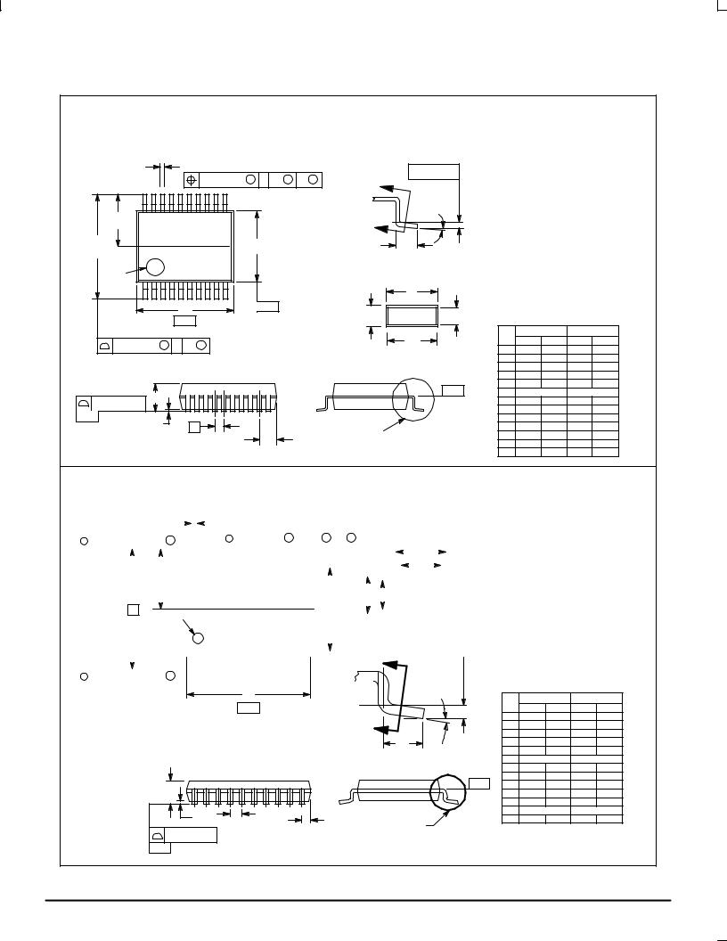
MOTOROLA |
|
|
|
|
|
|
|
|
6 |
|
|
|
|
|
|
|
|
|
|
|
|
|
|
|
|
|
|
|
|
|
|
|
|
MC54/74HCT373A |
||
|
|
|
|
|
|
|
|
|
|
OUTLINE DIMENSIONS |
|
|
|
|
|
|
|
|
|
|
|
|
|
|
|
|
|
|
SD SUFFIX |
|
|
|
|
|
|
|
|
|
|
|
|
|
|
|
|
PLASTIC SSOP PACKAGE |
|
|
|
|
|
|
|
|
|
|
|
|
|
|
|
|
|
|
CASE 940C±03 |
|
NOTES: |
|
|
|
|
|
|
|
|
|
|
|
|
|
|
|
ISSUE B |
|
|
|
|
|
|
|
|
|
|
|
|
|
|
|
|
|
|
1. DIMENSIONING AND TOLERANCING PER ANSI |
|||||
|
|
|
|
|
20X |
K REF |
|
|
|
|
|
|
Y14.5M, 1982. |
|
|
|
|
|
|
|
|
|
|
|
|
|
0.25 (0.010) |
2. CONTROLLING DIMENSION: MILLIMETER. |
|||||||
|
|
|
|
|
|
0.12 (0.005) M |
T |
U |
|
V |
3. DIMENSION A DOES NOT INCLUDE MOLD FLASH, |
||||||
|
|
|
|
|
|
S |
S |
|
|||||||||
|
|
|
|
|
|
|
PROTRUSIONS OR GATE BURRS. MOLD FLASH OR |
||||||||||
|
|
|
|
|
|
|
|
|
|
|
N |
|
GATE BURRS SHALL NOT EXCEED 0.15 (0.006) PER |
||||
|
|
|
|
|
|
|
|
|
|
|
|
|
|||||
|
|
|
|
|
|
|
|
|
|
|
|
|
SIDE. |
|
|
|
|
|
|
|
|
|
|
|
|
|
|
|
M |
|
4. DIMENSION B DOES NOT INCLUDE INTERLEAD |
||||
|
L/2 |
20 |
|
|
|
11 |
|
|
|
|
|
FLASH OR PROTRUSION. INTERLEAD FLASH OR |
|||||
|
|
|
|
|
|
|
|
N |
|
PROTRUSION SHALL NOT EXCEED 0.15 (0.006) PER |
|||||||
|
|
|
|
|
|
|
|
|
|
|
|
SIDE. |
|
|
|
|
|
|
|
|
|
|
|
|
B |
|
|
|
F |
|
5. DIMENSION K DOES NOT INCLUDE DAMBAR |
||||
L |
|
|
|
|
|
|
|
|
|
PROTRUSION/INTRUSION. ALLOWABLE DAMBAR |
|||||||
|
|
|
|
|
|
|
|
|
|
|
|
|
PROTRUSION SHALL BE 0.13 (0.005) TOTAL IN |
||||
|
|
|
|
|
|
|
|
|
|
|
DETAIL E |
|
EXCESS OF K DIMENSION AT MAXIMUM MATERIAL |
||||
|
PIN 1 |
1 |
|
|
|
10 |
|
|
|
|
|
CONDITION. DAMBAR INTRUSION SHALL NOT |
|||||
|
|
|
|
|
|
|
|
|
|
||||||||
|
IDENT |
|
|
|
|
|
|
|
|
|
REDUCE DIMENSION K BY MORE THAN 0.07 (0.002) |
||||||
|
|
|
|
|
|
|
|
|
|
|
|
||||||
|
|
|
|
|
|
|
|
|
|
|
K |
|
AT LEAST MATERIAL CONDITION. |
|
|||
|
|
|
|
|
|
|
|
|
|
|
|
6. TERMINAL NUMBERS ARE SHOWN FOR REFERENCE |
|||||
|
|
|
|
|
A |
|
±U± |
|
|
|
|
ONLY. |
|
|
|
|
|
|
|
|
|
|
|
|
|
J |
J1 |
7. DIMENSION A AND B ARE TO BE DETERMINED AT |
|||||||
|
|
|
|
|
|
|
|
|
|
||||||||
|
|
|
|
±V± |
|
|
|
|
|
DATUM PLANE ±W±. |
|
|
|||||
|
|
|
|
|
|
|
|
|
|
|
|
|
|
|
|
||
|
|
|
|
|
|
|
|
|
|
|
K1 |
|
|
MILLIMETERS |
INCHES |
||
|
0.20 (0.008) M |
T |
U |
S |
|
|
|
|
|
DIM |
MIN |
MAX |
MIN |
MAX |
|||
|
|
|
|
|
|
|
A |
7.07 |
7.33 |
0.278 |
0.288 |
||||||
|
|
|
|
|
|
|
|
|
|
|
|
|
|||||
|
|
|
|
|
|
|
|
|
|
|
SECTION N±N |
B |
5.20 |
5.38 |
0.205 |
0.212 |
|
|
|
|
|
|
|
|
|
|
|
|
C |
1.73 |
1.99 |
0.068 |
0.078 |
||
|
|
|
|
|
|
|
|
|
|
|
|
|
|||||
|
|
|
|
|
|
|
|
|
|
|
|
|
D |
0.05 |
0.21 |
0.002 |
0.008 |
|
|
|
|
|
|
|
|
|
|
|
|
±W± |
F |
0.63 |
0.95 |
0.024 |
0.037 |
|
|
|
C |
|
|
|
|
|
|
|
|
G |
0.65 BSC |
0.026 BSC |
|||
|
0.076 (0.003) |
|
|
|
|
|
|
|
|
|
H |
0.59 |
0.75 |
0.023 |
0.030 |
||
|
|
|
|
|
|
|
|
|
|
|
|||||||
±T± |
SEATING |
|
|
|
|
|
|
|
|
|
|
|
J |
0.09 |
0.20 |
0.003 |
0.008 |
|
|
|
|
|
|
|
|
|
|
|
J1 |
0.09 |
0.16 |
0.003 |
0.006 |
||
|
PLANE |
|
D |
|
G |
|
|
|
|
|
DETAIL E |
|
K |
0.25 |
0.38 |
0.010 |
0.015 |
|
|
|
|
|
|
|
|
|
|
||||||||
|
|
|
|
|
|
|
|
H |
|
|
|
K1 |
0.25 |
0.33 |
0.010 |
0.013 |
|
|
|
|
|
|
|
|
|
|
|
|
|
||||||
|
|
|
|
|
|
|
|
|
|
|
|
L |
7.65 |
7.90 |
0.301 |
0.311 |
|
|
|
|
|
|
|
|
|
|
|
|
|
|
|||||
|
|
|
|
|
|
|
|
|
|
|
|
|
M |
0 |
8 |
0 |
8 |
|
|
|
|
|
|
|
|
|
|
|
|
|
|
|
|
|
|
|
|
|
|
|
|
|
|
|
|
|
|
|
|
|
|
|
|
DT SUFFIX |
|
|
|
|
|
|
|
|
|
|
|
||||||||
|
|
|
|
|
|
|
|
|
|
|
|
|
|
|
|
|
|
|
|
|
|
|
|
|
|
|
|
|
PLASTIC TSSOP PACKAGE |
|
|
|
|||||||||||||||||||||||
|
|
|
|
|
|
|
|
|
|
|
|
|
|
|
|
|
|
|
|
|
|
|
|
|
|
|
|
|
|
|
|
|
|
|
CASE 948E±02 |
|
|
|
|||||||||||||||||
|
|
|
|
|
|
|
|
|
|
|
|
|
|
|
|
|
|
|
|
20X K REF |
|
|
|
|
|
|
|
|
|
|
|
ISSUE A |
|
|
|
|
|
|
|
|
|
NOTES: |
|||||||||||||
|
|
|
|
|
|
|
|
|
|
|
|
|
|
|
|
|
|
|
|
|
|
|
|
|
|
|
|
|
|
|
|
|
|
|
|
|
|
|
|||||||||||||||||
|
|
|
|
|
|
|
|
|
|
|
|
|
|
|
|
|
|
|
|
|
|
|
|
|
|
|
|
|
|
|
|
|
|
|
|
|
|
|
|
|
|
|
|
|
|
|
|
||||||||
|
|
|
|
|
|
|
|
|
|
|
|
|
|
|
|
|
|
|
|
|
|
|
|
|
|
|
|
|
|
|
|
|
|
|
|
|
|
|
|
|
|
|
|
|
|
|
|
|
|
|
|
|
1. |
DIMENSIONING AND TOLERANCING PER ANSI |
|
|
|
|
|
0.15 (0.006) |
T |
U S |
|
|
|
|
|
|
|
|
|
0.10 (0.004) M |
T |
U S |
V S |
|
|
|
|
|
|
|
|
|
|
|
|
|
|
|
|
Y14.5M, 1982. |
|||||||||||||||||||
|
|
|
|
|
|
|
|
|
|
|
|
|
|
|
|
|
|
|
|
|
|
|
|
|
|
|
|
|
|
|
|
|
|
|
|
|
|
|
|
|
|
|
|
|
|
|
|
|
K |
|
|
|
2. |
CONTROLLING DIMENSION: MILLIMETER. |
|
|
|
|
|
|
|
|
|
|
|
|
|
|
|
|
|
|
|
|
|
|
|
|
|
|
|
|
|
|
|
|
|
|
|
|
|
|
|
|
|
|
|
|
|
|
|
|
|
|
|
|
3. |
DIMENSION A DOES NOT INCLUDE MOLD FLASH, |
|||
|
|
|
|
|
|
|
|
|
|
|
|
|
|
|
|
|
|
|
|
|
|
|
|
|
|
|
|
|
|
|
|
|
|
|
|
|
|
|
|
|
|
|
|
|
|
|
|
|
K1 |
|
|
|
|
|
PROTRUSIONS OR GATE BURRS. MOLD FLASH |
|
|
|
|
|
|
|
|
2X L/2 |
|
20 |
|
|
|
|
|
|
|
|
|
|
11 |
|
|
|
|
|
|
|
|
|
|
|
|
|
|
|
|
|
|
|
|
|
|
|
OR GATE BURRS SHALL NOT EXCEED 0.15 |
||||||||||
|
|
|
|
|
|
|
|
|
|
|
|
|
|
|
|
|
|
|
|
|
|
|
|
|
|
|
|
|
|
|
|
|
|
|
|
|
|
|
|
|
|
|
|
|
|
|
|
|
|
|
(0.006) PER SIDE. |
||||
|
|
|
|
|
|
|
|
|
|
|
|
|
|
|
|
|
|
|
|
|
|
|
|
|
|
|
|
|
|
|
|
|
|
|
|
|
|
|
|
|
|
|
|
|
|
|
|
|
|||||||
|
|
|
|
|
|
|
|
|
|
|
|
|
|
|
|
|
|
|
|
|
|
|
|
|
|
|
|
|
|
|
|
|
|
|
|
|
|
|
|
|
|
|
|
|
|
|
|
|
|
|
|
|
4. |
DIMENSION B DOES NOT INCLUDE INTERLEAD |
|
|
|
|
|
|
|
|
|
|
|
|
|
|
|
|
|
|
|
|
|
|
|
|
|
|
|
|
|
|
|
|
|
|
|
|
|
|
|
|
|
J J1 |
|
|
|
|
|
|
|
|
|||||||
|
|
|
|
|
|
|
|
|
|
|
|
|
|
|
|
|
|
|
|
|
|
|
|
|
|
|
|
|
|
|
|
|
|
|
B |
|
|
|
|
|
|
|
|
|
|
|
FLASH OR PROTRUSION. INTERLEAD FLASH OR |
||||||||
|
|
|
|
|
|
|
|
|
|
|
|
|
|
|
|
|
|
|
|
|
|
|
|
|
|
|
|
|
|
|
|
|
|
|
|
|
|
|
|
|
|
|
|
|
|
|
|
|
|
|
PROTRUSION SHALL NOT EXCEED 0.25 (0.010) |
||||
|
|
|
|
|
L |
|
|
|
|
|
|
|
|
|
|
|
|
|
|
|
|
|
|
|
|
|
|
|
|
|
|
|
|
|
|
|
|
|
|
|
|
|
|
|
|
|
|
|
|||||||
|
|
|
|
|
|
|
|
|
|
|
|
|
|
|
|
|
|
|
|
|
|
|
|
|
|
|
|
|
|
|
|
|
|
|
|
|
|
|
|
|
|
|
|
|
|
|
|
|
|
|
|
|
|||
|
|
|
|
|
|
|
PIN 1 |
|
|
|
|
|
|
|
|
|
|
|
|
|
|
|
|
|
|
|
|
|
|
|
|
±U± |
|
|
|
|
|
|
|
|
|
|
|
|
|
|
|
|
|
PER SIDE. |
|||||
|
|
|
|
|
|
|
|
|
|
|
|
|
|
|
|
|
|
|
|
|
|
|
|
|
|
|
|
|
|
|
|
|
|
|
|
|
|
|
|
|
|
|
SECTION N±N |
5. |
DIMENSION K DOES NOT INCLUDE DAMBAR |
||||||||||
|
|
|
|
|
|
|
|
|
|
|
|
|
|
|
|
|
|
|
|
|
|
|
|
|
|
|
|
|
|
|
|
|
|
|
|
|
|
|
|
|
|
||||||||||||||
|
|
|
|
|
|
|
|
|
IDENT |
|
|
|
|
|
|
|
|
|
|
|
|
|
|
|
|
|
|
|
|
|
|
|
|
|
|
|
|
|
|
|
|
|
|
PROTRUSION. ALLOWABLE DAMBAR |
|||||||||||
|
|
|
|
|
|
|
|
|
|
|
|
|
|
|
|
|
|
|
|
|
|
|
|
|
|
|
|
|
|
|
|
|
|
|
|
|
|
|
|
|
|
|
|
|
|
|
|
|
|
|
|
|
|
|
PROTRUSION SHALL BE 0.08 (0.003) TOTAL IN |
|
|
|
|
|
|
|
|
|
|
|
|
|
1 |
|
|
|
|
|
|
|
|
|
|
|
10 |
|
|
|
|
|
|
|
|
|
|
|
|
|
|
|
|
|
|
|
|
|
|
|
EXCESS OF THE K DIMENSION AT MAXIMUM |
||||||
|
|
|
|
|
|
|
|
|
|
|
|
|
|
|
|
|
|
|
|
|
|
|
|
|
|
|
|
|
|
|
|
|
|
|
|
|
|
|
|
|
|
|
|
|
|
|
|
|
|
|
|
|
|
|
MATERIAL CONDITION. |
|
|
|
|
|
|
|
|
|
|
|
|
|
|
|
|
|
|
|
|
|
|
|
|
|
|
|
|
|
|
|
|
|
|
|
|
|
|
|
|
|
|
|
N |
|
0.25 (0.010) |
|
6. |
TERMINAL NUMBERS ARE SHOWN FOR |
|||||||
|
|
|
|
|
|
|
|
|
|
|
|
|
|
|
|
|
|
|
|
|
|
|
|
|
|
|
|
|
|
|
|
|
|
|
|
|
|
|
|
|
|
|
|
|
|
|
|
|
|
|
|
|
REFERENCE ONLY. |
||
|
|
|
|
|
|
|
|
|
|
|
|
|
|
|
|
|
|
|
|
|
|
|
|
|
|
|
|
|
|
|
|
|
|
|
|
|
|
|
|
|
|
|
|
|
|
|
|
|
|
|
|
|
|
|
|
|
|
|
|
0.15 (0.006) |
T |
U S |
|
|
|
|
|
|
|
|
|
|
|
|
|
|
|
|
|
|
|
|
|
|
|
|
|
|
|
|
|
|
|
|
|
|
|
|
|
|
|
|
|
7. |
DIMENSION A AND B ARE TO BE DETERMINED |
||||||
|
|
|
|
|
|
|
|
|
|
|
|
|
|
|
|
|
|
|
|
|
|
|
|
|
|
|
|
|
|
|
|
|
|
|
|
|
|
|
|
|
|
||||||||||||||
|
|
|
|
|
|
|
|
|
|
|
|
|
|
|
|
|
|
|
|
|
|
|
|
|
|
|
|
|
|
|
|
|
|
|
|
|
|
|
|
|
|
|
|
|
|
|
|
|
|
|
|
|
|
|
AT DATUM PLANE ±W±. |
|
|
|
|
|
|
|
|
|
|
|
|
|
|
|
|
|
|
|
|
|
|
|
|
|
|
|
|
|
|
|
|
|
|
|
|
|
|
|
|
|
|
|
|
|
|
|
|
|
|
|
|
|
|
|
|
|
A |
|
M |
|
MILLIMETERS |
INCHES |
||
|
|
|
|
|||||
|
±V± |
|
|
|
||||
|
|
|
DIM |
MIN |
MAX |
MIN |
MAX |
|
|
|
|
|
A |
6.40 |
6.60 |
0.252 |
0.260 |
|
|
|
N |
B |
4.30 |
4.50 |
0.169 |
0.177 |
|
|
|
F |
C |
±±± |
1.20 |
±±± |
0.047 |
|
|
|
D |
0.05 |
0.15 |
0.002 |
0.006 |
|
|
|
|
DETAIL E |
F |
0.50 |
0.75 |
0.020 |
0.030 |
|
|
|
G |
0.65 BSC |
0.026 BSC |
|||
|
|
|
|
H |
0.27 |
0.37 |
0.011 |
0.015 |
|
|
|
±W± |
J |
0.09 |
0.20 |
0.004 |
0.008 |
C |
|
|
J1 |
0.09 |
0.16 |
0.004 |
0.006 |
|
|
|
|
K |
0.19 |
0.30 |
0.007 |
0.012 |
|
|
|
|
|
|||||
|
|
|
|
K1 |
0.19 |
0.25 |
0.007 |
0.010 |
D |
|
G |
H |
L |
6.40 BSC |
0.252 BSC |
||
|
M |
0 |
8 |
0 |
8 |
|||
|
|
|||||||
0.100 (0.004) |
|
|
DETAIL E |
|
|
|
|
|
|
|
|
|
|
|
|
|
|
±T± SEATING |
|
|
|
|
|
|
|
|
PLANE |
|
|
|
|
|
|
|
|
7 |
MOTOROLA |

MC54/74HCT373A
Motorola reserves the right to make changes without further notice to any products herein. Motorola makes no warranty, representation or guarantee regarding the suitability of its products for any particular purpose, nor does Motorola assume any liability arising out of the application or use of any product or circuit, and specifically disclaims any and all liability, including without limitation consequential or incidental damages. ªTypicalº parameters can and do vary in different applications. All operating parameters, including ªTypicalsº must be validated for each customer application by customer's technical experts. Motorola does not convey any license under its patent rights nor the rights of others. Motorola products are not designed, intended, or authorized for use as components in systems intended for surgical implant into the body, or other applications intended to support or sustain life, or for any other application in which the failure of the Motorola product could create a situation where personal injury or death may occur. Should Buyer purchase or use Motorola products for any such unintended or unauthorized application, Buyer shall indemnify and hold Motorola and its officers, employees, subsidiaries, affiliates, and distributors harmless against all claims, costs, damages, and expenses, and reasonable attorney fees arising out of, directly or indirectly, any claim of personal injury or death associated with such unintended or unauthorized use, even if such claim alleges that Motorola was negligent regarding the design or manufacture of the part. Motorola and  are registered trademarks of Motorola, Inc. Motorola, Inc. is an Equal Opportunity/Affirmative Action Employer.
How to reach us: |
|
USA/EUROPE: Motorola Literature Distribution; |
JAPAN: Nippon Motorola Ltd.; Tatsumi±SPD±JLDC, Toshikatsu Otsuki, |
P.O. Box 20912; Phoenix, Arizona 85036. 1±800±441±2447 |
6F Seibu±Butsuryu±Center, 3±14±2 Tatsumi Koto±Ku, Tokyo 135, Japan. 03±3521±8315 |
MFAX: RMFAX0@email.sps.mot.com ±TOUCHTONE (602) 244±6609 |
HONG KONG: Motorola Semiconductors H.K. Ltd.; 8B Tai Ping Industrial Park, |
INTERNET: http://Design±NET.com |
51 Ting Kok Road, Tai Po, N.T., Hong Kong. 852±26629298 |
◊ CODELINE MC54/74HCT373A/D
*MC54/74HCT373A/D*