

motorola / 4HC4538A
.PDFMOTOROLA
SEMICONDUCTOR TECHNICAL DATA
Dual Precision
Monostable Multivibrator
(Retriggerable, Resettable)
The MC54/74HC4538A is identical in pinout to the MC14538B. The device inputs are compatible with standard CMOS outputs; with pullup resistors, they are compatible with LSTTL outputs.
This dual monostable multivibrator may be triggered by either the positive or the negative edge of an input pulse, and produces a precision output pulse over a wide range of pulse widths. Because the device has conditioned trigger inputs, there are no trigger±input rise and fall time restrictions. The output pulse width is determined by the external timing components, Rx and Cx. The device has a reset function which forces the Q output low and the Q output high, regardless of the state of the output pulse circuitry.
•Unlimited Rise and Fall Times Allowed on the Trigger Inputs
•Output Pulse is Independent of the Trigger Pulse Width
•±10% Guaranteed Pulse Width Variation from Part to Part (Using the Same Test Jig)
•Output Drive Capability: 10 LSTTL Loads
•Outputs Directly Interface to CMOS, NMOS and TTL
•Operating Voltage Range: 3.0 to 6.0 V
•Low Input Current: 1.0 μA
•High Noise Immunity Characteristic of CMOS Devices
•In Compliance with the Requirements Defined by JEDEC Standard No. 7A
•Chip Complexity: 145 FETs or 36 Equivalent Gates
LOGIC DIAGRAM
|
|
CX1 |
|
RX1 |
|
VCC |
|
|
|
|
|
|
|
|
|
|
|
|
|
|
|
1 |
2 |
|
|
|
|
|
|
TRIGGER |
A1 |
4 |
|
|
6 |
Q1 |
|
|
|
|
|
|
|
|
|
||||
5 |
|
|
|
|
|
|
|
||
INPUTS |
B1 |
|
|
7 |
Q1 |
CX2 |
RX2 |
|
|
|
|
|
|
|
|
VCC |
|||
|
|
3 |
|
|
|
|
|
|
|
RESET 1 |
|
|
|
|
15 |
14 |
|
||
|
|
|
|
|
|
|
|
||
|
|
TRIGGER |
A2 |
12 |
|
|
10 |
Q2 |
|
|
|
|
|
|
|||||
|
|
|
|
|
|
|
|||
|
|
INPUTS |
B2 11 |
|
|
9 |
Q2 |
||
|
|
|
|
|
|
|
|
|
|
RESET 2 13
PIN 16 = VCC
PIN 8 = GND
RX AND CX ARE EXTERNAL COMPONENTS
PIN 1 AND PIN 15 MUST BE HARD WIRED TO GND
MC54/74HC4538A
|
|
|
J SUFFIX |
16 |
|
CERAMIC PACKAGE |
|
|
|
CASE 620±10 |
|
|
1 |
|
|
|
|
|
N SUFFIX |
16 |
|
PLASTIC PACKAGE |
|
|
1 |
|
CASE 648±08 |
|
|
|
|
|
|
|
D SUFFIX |
16 |
|
SOIC PACKAGE |
|
|
1 |
CASE 751B±05 |
|
|
|
|
|
|
|
ORDERING INFORMATION |
|
|
MC54HCXXXXAJ |
Ceramic |
|
|
MC74HCXXXXAN |
Plastic |
|
|
MC74HCXXXXAD |
SOIC |
|
PIN ASSIGNMENT
|
GND |
1 |
16 |
VCC |
|
CX1/RX1 2 |
15 |
GND |
|
||
RESET 1 |
3 |
14 |
CX2/RX2 |
|
|
|
A1 |
4 |
13 |
RESET 2 |
|
|
B1 |
5 |
12 |
A2 |
|
|
Q1 |
6 |
11 |
B2 |
|
|
Q1 |
7 |
10 |
Q2 |
|
|
GND |
8 |
9 |
Q2 |
|
|
FUNCTION TABLE |
|
|||
|
Inputs |
|
|
Outputs |
|
Reset |
A |
|
B |
Q |
Q |
H |
|
|
H |
|
|
H |
L |
|
|
|
|
H |
X |
|
L |
Not Triggered |
|
H |
H |
|
X |
Not Triggered |
|
H |
L,H, |
|
H |
Not Triggered |
|
H |
L |
|
L,H, |
Not Triggered |
|
L |
X |
|
X |
L |
H |
|
X |
|
X |
Not Triggered |
|
10/95
Motorola, Inc. 1995 |
REV 6 |
MC54/74HC4538A
MAXIMUM RATINGS*
Symbol |
Parameter |
|
Value |
Unit |
|
|
|
|
|
VCC |
DC Supply Voltage (Referenced to GND) |
|
± 0.5 to + 7.0 |
V |
Vin |
DC Input Voltage (Referenced to GND) |
|
± 1.5 to VCC + 1.5 |
V |
|
||||
Vout |
DC Output Voltage (Referenced to GND) |
|
± 0.5 to VCC + 0.5 |
|
Iin |
DC Input Current, per Pin |
A, B, Reset |
± 20 |
mA |
|
|
Cx, Rx |
± 30 |
|
Iout |
DC Output Current, per Pin |
|
± 25 |
mA |
ICC |
DC Supply Current, VCC and GND Pins |
|
± 50 |
mA |
PD |
Power Dissipation in Still Air, Plastic or Ceramic DIP² |
750 |
mW |
|
|
SOIC Package² |
500 |
|
|
|
|
|
|
|
Tstg |
Storage Temperature |
|
± 65 to + 150 |
_C |
TL |
Lead Temperature, 1 mm from Case for 10 Seconds |
|
_C |
|
|
||||
|
(Plastic DIP or SOIC Package) |
260 |
|
|
|
(Ceramic DIP) |
300 |
|
|
|
|
|
|
|
This device contains protection circuitry to guard against damage due to high static voltages or electric fields. However, precautions must be taken to avoid applications of any voltage higher than maximum rated voltages to this high±impedance circuit. For proper operation, Vin and Vout should be constrained to the
range GND v (Vin or Vout) v VCC. Unused inputs must always be
tied to an appropriate logic voltage level (e.g., either GND or VCC). Unused outputs must be left open.
*Maximum Ratings are those values beyond which damage to the device may occur. Functional operation should be restricted to the Recommended Operating Conditions.
²Derating Ð Plastic DIP: ± 10 mW/ _C from 65_ to 125_C
Ceramic DIP: ± 10 mW/_C from 100_ to 125_C SOIC Package: ± 7 mW/_C from 65_ to 125_C
For high frequency or heavy load considerations, see Chapter 2 of the Motorola High±Speed CMOS Data Book (DL129/D).
RECOMMENDED OPERATING CONDITIONS
Symbol |
Parameter |
|
|
Min |
Max |
Unit |
|
|
|
|
|
|
|
VCC |
DC Supply Voltage (Referenced to GND) |
|
|
3.0** |
6.0 |
V |
Vin, Vout |
DC Input Voltage, Output Voltage (Referenced to GND) |
|
|
0 |
VCC |
V |
TA |
Operating Temperature, All Package Types |
|
|
± 55 |
+ 125 |
_C |
tr, tf |
Input Rise and Fall Time |
VCC = 2.0 |
V |
0 |
1000 |
ns |
|
(Figure 7) |
VCC = 4.5 |
V |
0 |
500 |
|
|
|
VCC = 6.0 V |
0 |
400 |
|
|
|
A or B (Figure 5) |
|
|
Ð |
No Limit |
|
|
|
|
|
|
|
|
Rx |
External Timing Resistor |
VCC < 4.5 |
V |
1.0 |
* |
kΩ |
|
|
VCC ≥ 4.5 |
V |
2.0 |
* |
|
Cx |
External Timing Capacitor |
|
|
0 |
* |
μF |
*The maximum allowable values of Rx and Cx are a function of the leakage of capacitor Cx, the leakage of the HC4538A, and leakage due to board layout and surface resistance. For most applications, Cx/Rx should be limited to a maximum value of 10 μF/1.0 MΩ. Values of Cx > 1.0 μF may cause a problem during power down (see Power Down Considerations). Susceptibility to externally induced noise signals may occur for Rx > 1.0 MΩ.
**The HC4538A will function at 2.0 V but for optimum pulse width stability, VCC should be above 3.0 V.
NOTE: Information on typical parametric values can be found in Chapter 2 of the Motorola High±Speed CMOS Data Book (DL129/D).
MOTOROLA |
3±2 |

|
|
|
|
|
|
|
|
MC54/74HC4538A |
|||||
DC CHARACTERISTICS FOR THE MC54/74HC4538A |
|
|
|
|
|
|
|
|
|
|
|
||
|
|
|
|
|
|
|
|
|
|
|
|
|
|
|
|
|
|
|
|
Guaranteed Limits |
|
|
|
|
|||
|
|
|
|
|
|
|
|
|
|
|
|
|
|
|
|
|
|
± 55 to |
|
|
|
|
|
|
|
|
|
|
|
|
VCC |
25_C |
|
v 85_C |
|
v 125_C |
|
|
|||
|
|
|
|
|
|
|
|
|
|
|
|
|
|
Symbol |
Parameter |
Test Conditions |
Volts |
Min |
Max |
|
Min |
Max |
|
Min |
Max |
Unit |
|
|
|
|
|
|
|
|
|
|
|
|
|
|
|
VIH |
Minimum High±Level |
Vout = 0.1 V or VCC ± 0.1 V |
2.0 |
1.5 |
|
|
1.5 |
|
|
1.5 |
|
V |
|
|
Input Voltage |
|Iout| v 20 μA |
4.5 |
3.15 |
|
|
3.15 |
|
|
3.15 |
|
|
|
|
|
|
6.0 |
4.2 |
|
|
4.2 |
|
|
4.2 |
|
|
|
|
|
|
|
|
|
|
|
|
|
|
|
|
|
VIL |
Maximum Low±Level |
Vout = 0.1 V or VCC ± 0.1 V |
2.0 |
|
0.5 |
|
|
0.5 |
|
|
0.5 |
V |
|
|
Input Voltage |
|Iout| v 20 μA |
4.5 |
|
1.35 |
|
|
1.35 |
|
|
1.35 |
|
|
|
|
|
6.0 |
|
1.8 |
|
|
1.8 |
|
|
1.8 |
|
|
|
|
|
|
|
|
|
|
|
|
|
|
|
|
VOH |
Minimum High±Level |
Vin = VIH or VIL |
2.0 |
1.9 |
|
|
1.9 |
|
|
1.9 |
|
V |
|
|
Output Voltage |
|Iout| v 20 μA |
4.5 |
4.4 |
|
|
4.4 |
|
|
4.4 |
|
|
|
|
|
|
6.0 |
5.9 |
|
|
5.9 |
|
|
5.9 |
|
|
|
|
|
|
|
|
|
|
|
|
|
|
|
|
|
|
|
Vin = VIH or VIL |
|
|
|
|
|
|
|
|
|
|
|
|
|
|Iout| v ± 4.0 mA |
4.5 |
3.98 |
|
|
3.84 |
|
|
3.7 |
|
|
|
|
|
|Iout| v ± 5.2 mA |
6.0 |
5.48 |
|
|
5.34 |
|
|
5.2 |
|
|
|
VOL |
Maximum Low±Level |
Vin = VIH or VIL |
2.0 |
|
0.1 |
|
|
0.1 |
|
|
0.1 |
V |
|
|
Output Voltage |
|Iout| v 20 μA |
4.5 |
|
0.1 |
|
|
0.1 |
|
|
0.1 |
|
|
|
|
|
6.0 |
|
0.1 |
|
|
0.1 |
|
|
0.1 |
|
|
|
|
|
|
|
|
|
|
|
|
|
|
|
|
|
|
Vin = VIH or VIL |
|
|
|
|
|
|
|
|
|
|
|
|
|
|Iout| v 4.0 mA |
4.5 |
|
0.26 |
|
|
0.33 |
|
|
0.4 |
|
|
|
|
|Iout| v 5.2 mA |
6.0 |
|
0.26 |
|
|
0.33 |
|
|
0.4 |
|
|
Iin |
Maximum Input |
Vin = VCC or GND |
6.0 |
|
± 0.1 |
|
|
± 1.0 |
|
|
± 1.0 |
μA |
|
|
Leakage Current |
|
|
|
|
|
|
|
|
|
|
|
|
|
(A, B, Reset) |
|
|
|
|
|
|
|
|
|
|
|
|
|
|
|
|
|
|
|
|
|
|
|
|
|
|
Iin |
Maximum Input |
Vin = VCC or GND |
6.0 |
|
± 50 |
|
|
± 500 |
|
|
± 500 |
nA |
|
|
Leakage Current |
|
|
|
|
|
|
|
|
|
|
|
|
|
(Rx, Cx) |
|
|
|
|
|
|
|
|
|
|
|
|
ICC |
Maximum Quiescent |
Vin = VCC or GND |
6.0 |
|
130 |
|
|
220 |
|
|
350 |
μA |
|
|
Supply Current |
Q1 and Q2 = Low |
|
|
|
|
|
|
|
|
|
|
|
|
(per package) |
Iout = 0 μA |
|
|
|
|
|
|
|
|
|
|
|
|
Standby State |
|
|
|
|
|
|
|
|
|
|
|
|
|
|
|
|
|
|
|
|
|
|
|
|
|
|
|
|
|
|
|
|
|
|
|
|
|
|||
ICC |
Maximum Supply Current |
Vin = VCC or GND |
|
|
|
|
± 45_C to |
|
± 55_C to |
|
|
||
|
(per package) |
Q1 and Q2 = High |
|
25_C |
|
85_C |
|
125_C |
|
|
|||
|
Active State |
Iout = 0 μA |
|
|
|
|
|
|
|
|
|
|
|
|
|
|
|
|
|
|
|
|
|
|
|
||
|
|
Pins 2 and 14 = 0.5 VCC |
6.0 |
|
400 |
|
|
600 |
|
|
800 |
μA |
|
3±3 |
MOTOROLA |
MC54/74HC4538A
AC CHARACTERISTICS FOR THE MC54/74HC4538A (CL = 50 pF, Input tr = tf = 6.0 ns)
|
|
|
|
|
|
Guaranteed Limits |
|
|
|
|||
|
|
|
|
|
|
|
|
|
|
|
|
|
|
|
|
|
± 55 to |
|
|
|
|
|
|
|
|
|
|
|
VCC |
25_C |
|
v 85_C |
|
v 125_C |
|
|||
|
|
|
|
|
|
|
|
|
|
|
|
|
Symbol |
Parameter |
|
Volts |
Min |
Max |
|
Min |
Max |
|
Min |
Max |
Unit |
|
|
|
|
|
|
|
|
|
|
|
|
|
tPLH |
Maximum Propagation Delay |
|
2.0 |
|
175 |
|
|
220 |
|
|
265 |
ns |
|
|
|
|
|
|
|||||||
|
Input A or B to Q |
|
4.5 |
|
35 |
|
|
44 |
|
|
53 |
|
|
(Figures 6 and 8) |
|
6.0 |
|
30 |
|
|
37 |
|
|
45 |
|
|
|
|
|
|
|
|
|
|
|
|
|
|
tPHL |
Maximum Propagation Delay |
|
2.0 |
|
195 |
|
|
245 |
|
|
295 |
ns |
|
Input A or B to NQ |
|
4.5 |
|
39 |
|
|
49 |
|
|
59 |
|
|
(Figures 6 and 8) |
|
6.0 |
|
33 |
|
|
42 |
|
|
50 |
|
|
|
|
|
|
|
|
|
|
|
|
|
|
tPHL |
Maximum Propagation Delay |
|
2.0 |
|
175 |
|
|
220 |
|
|
265 |
ns |
|
Reset to Q |
|
4.5 |
|
35 |
|
|
44 |
|
|
53 |
|
|
(Figures 7 and 8) |
|
6.0 |
|
30 |
|
|
37 |
|
|
45 |
|
|
|
|
|
|
|
|
|
|
|
|
|
|
tPLH |
Maximum Propagation Delay |
|
2.0 |
|
175 |
|
|
220 |
|
|
265 |
ns |
|
Reset to NQ |
|
4.5 |
|
35 |
|
|
44 |
|
|
53 |
|
|
(Figures 7 and 8) |
|
6.0 |
|
30 |
|
|
37 |
|
|
45 |
|
|
|
|
|
|
|
|
|
|
|
|
|
|
tTLH |
Maximum Output Transition Time, Any Output |
|
2.0 |
|
75 |
|
|
95 |
|
|
110 |
ns |
tTHL |
(Figures 7 and 8) |
|
4.5 |
|
15 |
|
|
19 |
|
|
22 |
|
|
|
|
6.0 |
|
13 |
|
|
16 |
|
|
19 |
|
|
|
|
|
|
|
|
|
|
|
|
|
|
Cin |
Maximum Input Capacitance |
(A. B, Reset) |
Ð |
|
10 |
|
|
10 |
|
|
10 |
pF |
|
|
(Cx, Rx) |
|
|
25 |
|
|
25 |
|
|
25 |
|
NOTE: For propagation delays with loads other than 50 pF, and information on typical parametric values, see Chapter 2 of the Motorola High± Speed CMOS Data Book (DL129/D).
|
|
Typical @ 25°C, VCC = 5.0 V |
|
CPD |
Power Dissipation Capacitance (Per Multivibrator)* |
150 |
pF |
*Used to determine the no±load dynamic power consumption: PD = CPD VCC2f + ICC VCC. For load considerations, see Chapter 2 of the Motorola High±Speed CMOS Data Book (DL129/D).
TIMING CHARACTERISTICS FOR THE MC54/74HC4538A (Input tr = tf = 6.0 ns)
|
|
|
|
|
Guaranteed Limits |
|
|
|
|||
|
|
|
|
|
|
|
|
|
|
|
|
|
|
|
± 55 to |
|
|
|
|
|
|
|
|
|
|
VCC |
25_C |
|
v 85_C |
|
v 125_C |
|
|||
|
|
|
|
|
|
|
|
|
|
|
|
Symbol |
Parameter |
Volts |
Min |
Max |
|
Min |
Max |
|
Min |
Max |
Unit |
|
|
|
|
|
|
|
|
|
|
|
|
trec |
Minimum Recovery Time, Inactive to A or B |
2.0 |
0 |
|
|
0 |
|
|
0 |
|
ns |
|
(Figure 7) |
4.5 |
0 |
|
|
0 |
|
|
0 |
|
|
|
|
6.0 |
0 |
|
|
0 |
|
|
0 |
|
|
|
|
|
|
|
|
|
|
|
|
|
|
tw |
Minimum Pulse Width, Input A or B |
2.0 |
60 |
|
|
75 |
|
|
90 |
|
ns |
|
(Figure 6) |
4.5 |
12 |
|
|
15 |
|
|
18 |
|
|
|
|
6.0 |
10 |
|
|
13 |
|
|
15 |
|
|
|
|
|
|
|
|
|
|
|
|
|
|
tw |
Minimum Pulse Width, Reset |
2.0 |
60 |
|
|
75 |
|
|
90 |
|
ns |
|
(Figure 7) |
4.5 |
12 |
|
|
15 |
|
|
18 |
|
|
|
|
6.0 |
10 |
|
|
13 |
|
|
15 |
|
|
|
|
|
|
|
|
|
|
|
|
|
|
tr, tf |
Maximum Input Rise and Fall Times, Reset |
2.0 |
|
1000 |
|
|
1000 |
|
|
1000 |
ns |
|
(Figure 7) |
4.5 |
|
500 |
|
|
500 |
|
|
500 |
|
|
|
6.0 |
|
400 |
|
|
400 |
|
|
400 |
|
|
|
|
|
|
|
|
|
|
|
|
|
|
A or B |
2.0 |
|
|
|
|
|
|
|
|
|
|
(Figure 7) |
4.5 |
|
|
|
No Limit |
|
|
|
||
|
|
6.0 |
|
|
|
|
|
|
|
|
|
|
|
|
|
|
|
|
|
|
|
|
|
MOTOROLA |
3±4 |

|
|
|
|
|
|
|
|
|
|
MC54/74HC4538A |
||||
OUTPUT PULSE WIDTH CHARACTERISTICS (CL = 50 pF)t |
|
|
|
|
|
|
|
|
|
|
|
|
||
|
|
|
|
|
|
|
|
|
|
|
|
|
||
|
|
Conditions |
|
|
|
Guaranteed Limits |
|
|
|
|||||
|
|
|
|
|
|
|
|
|
|
|
|
|
|
|
|
|
|
|
± 55 to |
|
|
|
|
|
|
|
|
|
|
|
|
|
VCC |
25_C |
|
v 85_C |
|
v 125_C |
|
|
||||
|
|
|
|
|
|
|
|
|
|
|
|
|
|
|
Symbol |
Parameter |
Timing Components |
Volts |
Min |
Max |
|
Min |
|
Max |
|
Min |
Max |
Unit |
|
|
|
|
|
|
|
|
|
|
|
|
|
|
|
|
τ |
Output Pulse Width* |
Rx = 10 kΩ, Cx = 0.1 μF |
5.0 |
0.63 |
0.77 |
|
0.6 |
|
0.8 |
|
0.59 |
0.81 |
ms |
|
|
(Figures 6 and 8) |
|
|
|
|
|
|
|
|
|
|
|
|
|
|
|
|
|
|
|
|
|
|
|
|
|
|
|
|
Ð |
Pulse Width Match |
Ð |
Ð |
|
|
± 5.0 |
|
|
|
% |
|
|||
|
Between Circuits in the |
|
|
|
|
|
|
|
|
|
|
|
|
|
|
same Package |
|
|
|
|
|
|
|
|
|
|
|
|
|
|
|
|
|
|
|
|
|
|
|
|
|
|
|
|
Ð |
Pulse Width Match |
Ð |
Ð |
|
|
|
|
± 10 |
|
|
|
% |
|
|
|
Variation (Part to Part) |
|
|
|
|
|
|
|
|
|
|
|
|
|
|
|
|
|
|
|
|
|
|
|
|
|
|
|
|
* For output pulse widths greater than 100 μs, typically τ = kRxCx, where the value of k may be found in Figure 1.
k, OUTPUT PULSE WIDTH CONSTANT (TYPICAL)
0.8
TA = 25°C
0.7
0.6
0.5
0.4
0.3
1 |
2 |
3 |
4 |
5 |
6 |
7 |
|
|
VCC, POWER SUPPLY VOLTAGE (VOLTS) |
|
|
||
Figure 1. Typical Output Pulse Width Constant, k, versus Supply Voltage
(For output pulse widths > 100 μs: τ = kRxCx)
|
10 s |
|
|
|
|
|
|
|
|
|
1 s VCC = 5 V, TA = 25°C |
|
|
|
|
|
|||
(τ ) |
100 ms |
|
|
|
|
|
|
|
|
WIDTH |
|
|
|
|
|
|
|
|
|
10 ms |
|
|
|
|
|
|
|
|
|
PULSE |
|
|
|
|
|
|
|
|
|
1 ms |
|
|
|
|
|
|
|
|
|
|
|
|
|
|
|
|
|
|
|
OUTPUT |
100 μs |
1 MΩ |
|
|
|
|
|
|
|
10 μs |
100 kΩ |
|
|
|
|
|
|
||
|
1 μs |
10 kΩ |
|
|
|
|
|
|
|
|
|
|
|
|
|
|
|
|
|
|
100 ns |
1 kΩ |
|
|
|
|
|
|
|
|
|
|
|
|
|
|
|
|
|
|
0.00001 |
0.0001 |
0.001 |
0.01 |
0.1 |
1 |
10 |
100 |
|
CAPACITANCE (μF)
Figure 2. Output Pulse Width versus
Timing Capacitance
(NORMALIZED TO 5 V NUMBER)
OUTPUT PULSE WIDTH (t)
1.1
R = 100 kΩ |
TA = 25°C |
x |
|
1 Cx = 1000 pF |
|
0.9
0.8
Rx = 1 MΩ
0.7Cx = 0.1 μF
0.6
0.5
1 |
2 |
3 |
4 |
5 |
6 |
7 |
|
|
VCC, POWER SUPPLY VOLTAGE (VOLTS) |
|
|
||
Figure 3. Normalized Output Pulse Width
versus Power Supply Voltage
3±5 |
MOTOROLA |

MC54/74HC4538A
|
|
1.1 |
|
|
|
|
|
|
|
|
|
OUTPUT PULSE WIDTH (τ ) |
(NORMALIZED TO 25°C NUMBER) |
1.05 |
|
|
|
|
|
|
|
|
|
1 |
|
|
|
|
|
|
|
|
|
||
0.95 |
VCC = 6 V |
|
|
|
|
Rx = 10 kΩ |
|
||||
|
|
|
|
|
|
Cx = 0.1 μF |
|
||||
0.9 |
|
|
|
|
|
|
|
|
|
||
0.85 |
|
VCC = 3 V |
|
|
|
|
|
|
|
||
|
|
|
|
|
|
|
|
|
|
|
|
|
|
0.8 |
|
|
|
|
|
|
|
|
|
|
|
± 75 |
± 50 |
± 25 |
0 |
25 |
50 |
75 |
100 |
125 |
150 |
|
|
|
|
TA, AMBIENT TEMPERATURE (°C) |
|
|
|||||
Figure 4. Normalized Output Pulse Width
versus Power Supply Voltage
|
|
1.03 |
|
|
|
|
|
|
|
|
|
|
(NORMALIZED TO 25°C NUMBER) |
1.02 |
Rx = 10 kΩ |
|
|
|
|
|
|
|
|
OUTPUT PULSE WIDTH (τ ) |
|
Cx = 0.1 μF |
|
|
|
|
|
|
|
||
1.01 |
|
|
|
|
|
|
|
|
|
||
1 |
|
|
|
|
|
|
|
|
|
||
0.99 |
VCC = 5.5 V |
|
|
|
|
|
|
|
|||
|
|
|
|
|
|
|
|
|
|||
0.98 |
|
VCC = 4.5 V |
VCC = 5 V |
|
|
|
|
|
|||
|
|
0.97 |
|
|
|
|
|
|
|
||
|
|
|
|
|
|
|
|
|
|
|
|
|
|
± 75 |
± 50 |
± 25 |
0 |
25 |
50 |
75 |
100 |
125 |
150 |
|
|
|
|
TA, AMBIENT TEMPERATURE (°C) |
|
|
|
||||
Figure 5. Normalized Output Pulse Width
versus Power Supply Voltage
MOTOROLA |
3±6 |

|
|
|
|
MC54/74HC4538A |
|
|
SWITCHING WAVEFORMS |
|
|
|
tw(H) |
|
|
|
|
50% |
|
|
VCC |
|
|
|
|
|
A |
|
|
|
GND |
|
|
|
tw(L) |
|
B |
|
|
50% |
VCC |
|
|
|
|
|
|
|
|
|
GND |
|
tPLH |
τ |
tPLH |
τ |
|
50% |
|
|
|
Q |
|
|
|
|
|
tPHL |
τ |
tPHL |
τ |
Q |
|
|
|
|
|
|
50% |
|
|
tr |
tf |
|
Figure 6. |
|
|
|
|
||
|
90% |
|
|
VCC |
|
|
|
|
|
A |
10% |
|
|
GND |
|
|
|
|
trr |
|
|
|
50% |
VCC |
|
|
|
GND |
|
B |
|
|
|
|
|
tf |
|
tf |
|
|
|
|
90% |
VCC |
RESET |
|
50% |
|
|
|
10% |
GND |
||
|
|
|
||
|
|
|
|
|
tTLH |
|
tw(L) |
trec |
τ + trr |
|
tPHL |
|
||
|
|
|
|
|
|
90% |
50% |
50% |
(RETRIGGERED PULSE) |
|
10% |
|
||
Q |
|
|
|
|
tTHL |
|
tPLH |
|
|
Q |
90% |
|
|
|
|
50% |
|
|
|
|
10% |
|
|
|
|
|
|
|
|
Figure 7.
|
TEST POINT |
||||||||
|
|
|
|
|
|
|
|
|
|
|
OUTPUT |
|
|
|
|
|
|||
DEVICE |
|
|
|
|
|
|
|
|
|
|
|
|
|
|
|
|
|
|
|
UNDER |
|
|
|
|
|
|
|
|
CL* |
TEST |
|
|
|
|
|
|
|
|
|
|
|
|
|
|
|
|
|||
|
|
|
|
||||||
|
|
|
|
|
|
|
|
|
|
|
|
|
|
|
|
|
|
|
|
|
|
|
|
|
|
|
|
|
|
|
|
|
|
|
|
|
|
|
|
|
|
|
|
|
|
|
|
|
|
|
|
|
|
|
|
|
|
|
|
* Includes all probe and jig capacitance
Figure 8. Test Circuit
3±7 |
MOTOROLA |

MC54/74HC4538A
PIN DESCRIPTIONS
INPUTS
A1, A2 (Pins 4, 12)
Positive±edge trigger inputs. A rising±edge signal on either of these pins triggers the corresponding multivibrator when there is a high level on the B1 or B2 input.
B1, B2 (Pins 5, 11)
Negative±edge trigger inputs. A falling±edge signal on either of these pins triggers the corresponding multivibrator when there is a low level on the A1 or A2 input.
tors (see the Block Diagram). Polystyrene capacitors are recommended for optimum pulse width control. Electrolytic capacitors are not recommended due to high leakages associated with these type capacitors.
GND (Pins 1 and 15)
External ground. The external timing capacitors discharge to ground through these pins.
OUTPUTS
Q1, Q2 (Pins 6, 10)
Reset 1, Reset 2 (Pins 3, 13)
Reset inputs (active low). When a low level is applied to one of these pins, the Q output of the corresponding multivibrator is reset to a low level and the Q output is set to a high level.
CX1/RX1 and CX2/RX2 (Pins 2 and 14)
External timing components. These pins are tied to the common points of the external timing resistors and capaci-
Noninverted monostable outputs. These pins (normally low) pulse high when the multivibrator is triggered at either the A or the B input. The width of the pulse is determined by the external timing components, RX and CX.
Q1, Q2 (Pins 7, 9)
Inverted monostable outputs. These pins (normally high) pulse low when the multivibrator is triggered at either the A or the B input. These outputs are the inverse of Q1 and Q2.
|
LOGIC DETAIL |
||
|
(1/2 THE DEVICE) |
||
|
RxCx |
|
|
|
UPPER |
|
|
|
REFERENCE |
OUTPUT |
|
|
CIRCUIT |
LATCH |
|
VCC |
± |
|
|
+ |
|
||
|
Vre, UPPER |
|
|
M1 |
LOWER |
|
|
REFERENCE |
|
||
VCC |
|
||
2 kΩ |
CIRCUIT |
|
|
± |
|
||
M2 |
|
||
+ |
Q |
||
|
|
||
M3 |
Vre, LOWER |
|
|
|
|
||
|
|
Q |
|
|
TRIGGER CONTROL |
||
A |
CIRCUIT |
|
|
C |
Q |
||
|
|||
|
|
TRIGGER CONTROL |
|
B |
CB R |
RESET CIRCUIT |
|
|
|||
RESET |
|
|
|
|
POWER |
|
|
|
ON |
|
|
|
RESET |
RESET LATCH |
|
|
|
||
Figure 9.
MOTOROLA |
3±8 |

MC54/74HC4538A
CIRCUIT OPERATION
Figure 12 shows the HC4538A configured in the retriggerable mode. Briefly, the device operates as follows (refer to Figure 10): In the quiescent state, the external timing capacitor, Cx, is charged to VCC. When a trigger occurs, the Q output goes high and Cx discharges quickly to the lower reference voltage (Vref Lower [1/3 VCC). Cx then charges, through Rx, back up to the upper reference voltage (Vref Upper [ 2/3 VCC), at which point the one±shot has timed out and the Q output goes low.
The following, more detailed description of the circuit operation refers to both the logic detail (Figure 9) and the timing diagram (Figure 10).
QUIESCENT STATE
In the quiescent state, before an input trigger appears, the output latch is high and the reset latch is high (#1 in Figure 10). Thus the Q output (pin 6 or 10) of the monostable multivibrator is low (#2, Figure 10).
The output of the trigger±control circuit is low (#3), and transistors M1, M2, and M3 are turned off. The external timing capacitor, Cx, is charged to VCC (#4), and both the upper and lower reference circuit has a low output (#5).
In addition, the output of the trigger±control reset circuit is low.
TRIGGER OPERATION
The HC4538A is triggered by either a rising±edge signal at input A (#7) or a falling±edge signal at input B (#8), with the unused trigger input and the Reset input held at the voltage levels shown in the Function Table. Either trigger signal will cause the output of the trigger±control circuit to go high (#9).
The trigger±control circuit going high simultaneously initiates two events. First, the output latch goes low, thus taking the Q output of the HC4538A to a high state (#10). Second, transistor M3 is turned on, which allows the external timing capacitor, Cx, to rapidly discharge toward ground (#11). (Note that the voltage across Cx appears at the input of both the upper and lower reference circuit comparator).
When Cx discharges to the reference voltage of the lower reference circuit (#12), the outputs of both reference circuits will be high (#13). The trigger±control reset circuit goes high, resetting the trigger±control circuit flip±flop to a low state (#14). This turns transistor M3 off again, allowing Cx to begin to charge back up toward VCC, with a time constant t = RxCx (#15). Once the voltage across Cx charges to above the lower reference voltage, the lower reference circuit will go low allowing the monostable multivibrator to be retriggered.
|
QUIESCENT |
|
TRIGGER CYCLE |
TRIGGER CYCLE |
|
|
|
|
STATE |
|
|
(A INPUT) |
(B INPUT) |
RESET |
RETRIGGER |
|
7 |
|
|
|
|
|
trr |
TRIGGER INPUT A |
|
|
|
|
|
|
|
(PIN 4 OR 12) |
|
|
|
|
|
|
|
TRIGGER INPUT B |
|
|
|
|
|
|
|
(PIN 5 OR 11) |
|
|
|
8 |
|
|
24 |
|
|
9 |
|
|
|
|
|
|
|
|
|
|
|
|
|
TRIGGER-CONTROL |
3 |
|
14 |
|
|
|
|
CIRCUIT OUTPUT |
|
|
|
|
|
|
|
|
4 |
11 |
15 |
17 |
21 |
23 |
|
RX/CX INPUT |
|
|
|
|
|
||
12 |
|
|
|
|
|
|
|
(PIN 2 OR 14) |
|
|
|
Vref UPPER |
|
|
|
Vref LOWER |
13 |
|
|
|
25 |
||
|
|
|
|
|
|||
|
|
|
|
|
|
||
UPPER REFERENCE |
5 |
|
|
18 |
|
|
|
CIRCUIT |
|
|
|
|
|
|
|
|
|
13 |
|
|
|
|
|
LOWER REFERENCE |
6 |
|
16 |
|
|
|
|
CIRCUIT |
|
|
|
|
|
|
|
RESET INPUT |
|
|
|
|
20 |
|
|
(PIN 3 OR 13) |
|
|
|
|
|
|
|
|
|
|
|
|
|
|
|
|
1 |
|
|
|
|
|
|
RESET LATCH |
|
|
|
|
22 |
|
|
|
|
10 |
|
|
|
|
|
Q OUTPUT |
2 |
|
|
19 |
|
|
|
(PIN 6 OR 10) |
|
|
τ |
|
τ |
|
τ + trr |
|
|
|
|
|
|||
Figure 10. Timing Diagram
3±9 |
MOTOROLA |
MC54/74HC4538A
When Cx charges up to the reference voltage of the upper reference circuit (#17), the output of the upper reference circuit goes low (#18). This causes the output latch to toggle, taking the Q output of the HC4538A to a low state (#19), and completing the time±out cycle.
POWER±DOWN CONSIDERATIONS
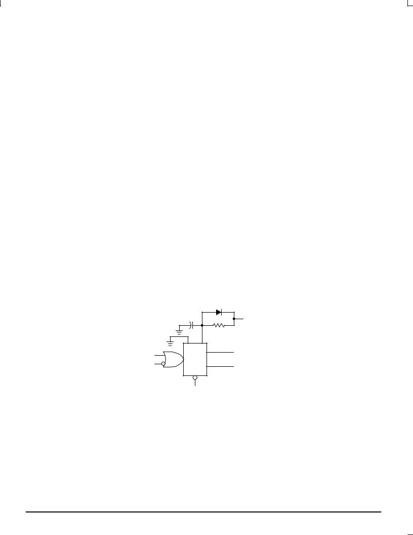
Large values of Cx may cause problems when powering down the HC4538A because of the amount of energy stored in the capacitor. When a system containing this device is powered down, the capacitor may discharge from VCC through the input protection diodes at pin 2 or pin 14. Current through the protection diodes must be limited to 30 mA; therefore, the turn±off time of the VCC power supply must not be faster than t = V CC C x /(30 mA). For example, if VCC = 5.0 V and Cx = 15 μF, the VCC supply must turn off no faster than t = (5.0 V) (15 μF)/30 mA = 2.5 ms. This is usually not a problem because power supplies are heavily filtered and cannot discharge at this rate.
When a more rapid decrease of VCC to zero volts occurs, the HC4538A may sustain damage. To avoid this possibility, use an external damping diode, Dx, connected as shown in Figure 11. Best results can be achieved if diode Dx is chosen to be a germanium or Schottky type diode able to withstand large current surges.
RESET AND POWER ON RESET OPERATION
A low voltage applied to the Reset pin always forces the Q output of the HC4538A to a low state.
The timing diagram illustrates the case in which reset occurs (#20) while Cx is charging up toward the reference voltage of the upper reference circuit (#21). When a reset
occurs, the output of the reset latch goes low (#22), turning on transistor M1. Thus Cx is allowed to quickly charge up to VCC (#23) to await the next trigger signal.
On power up of the HC4538A the power±on reset circuit will be high causing a reset condition. This will prevent the trigger±control circuit from accepting a trigger input during this state. The HC4538A's Q outputs are low and the Q not outputs are high.
RETRIGGER OPERATION
When used in the retriggerable mode (Figure 12), the HC4538A may be retriggered during timing out of the output pulse at any time after the trigger±control circuit flip±flop has been reset (#24), and the voltage across Cx is above the lower reference voltage. As long as the Cx voltage is below the lower reference voltage, the reset of the flip±flop is high, disabling any trigger pulse. This prevents M3 from turning on during this period resulting in an output pulse width that is predictable.
The amount of undershoot voltage on RxCx during the trigger mode is a function of loop delay, M3 conductivity, and VDD. Minimum retrigger time, trr (Figure 7), is a function of 1) time to discharge RxCx from VDD to lower reference
voltage (Tdischarge); 2) loop delay (Tdelay); 3) time to charge RxCx from the undershoot voltage back to the lower refer-
ence voltage (Tcharge).
Figure 13 shows the device configured in the non±retriggerable mode.
An Application Note (AN1558/D) titled Characterization of Retrigger Time in the HC4538A Dual Precision Monstable Multivibrator is being prepared. Please consult the factory for its availability.
|
DX |
CX |
V |
|
CC |
|
RX |
A |
Q |
|
|
B |
Q |
|
RESET
Figure 11. Discharge Protection During Power Down
MOTOROLA |
3±10 |