

motorola / 62v256
.pdfHM62V256 Series
32,768-word × 8-bit Low Voltage Operation CMOS Static RAM
ADE-203-136E (Z)
Rev. 5.0
Jun. 19, 1995
Features
∙Low voltage operation SRAM
Operating Supply Voltage: 2.7 V to 3.6 V
∙0.8 μm Hi-CMOS process
∙High speed
Access time: 70/85/100 ns (max)
∙Low power
Standby: 0.15 μW (typ)
∙Completely static memory
No clock or timing strobe required
∙Directly LVTTL compatible: All inputs and outputs
Ordering Information
Type No. |
Access Time |
Package |
HM62V256LFP-10T |
100 ns |
450 mil 280 pin plastic SOP (FP-28DA) |
HM62V256LFP-7SLT |
70 ns |
|
HM62V256LFP-10SLT |
100 ns |
|
HM62V256LFP-8ULT |
85 ns |
8 mm × 14 mm 32 pin TSOP (normal type) (TFP-32DA) |
HM62V256LT-10 |
100 ns |
|
HM62V256LT-8SL |
85 ns |
8 mm × 13.4 mm 28-pin TSOP (normal type) (TFP-28DA) |
HM62V256LTM-10 |
100 ns |
|
HM62V256LTM-7SL |
70 ns |
|
HM62V256LTM-10SL |
100 ns |
|
HM62V256LTM-8UL |
85 ns |
|
|
|
|

HM62V256 Series
Pin Arrangement
|
|
|
|
HM62W256LFP Series |
|
|
|
|
|
|
|
|
|
A14 |
1 |
28 |
VCC |
|
|||
|
|
|
A12 |
2 |
27 |
WE |
|
|
|
|
|
|
|
A7 |
3 |
26 |
A13 |
|
|||
|
|
|
A6 |
4 |
25 |
A8 |
|
|||
|
|
|
A5 |
5 |
24 |
A9 |
|
|||
|
|
|
A4 |
6 |
23 |
A11 |
|
|||
|
|
|
|
7 |
22 |
|
|
|
||
|
|
|
A3 |
OE |
|
|
|
|||
|
|
|
A2 |
8 |
21 |
A10 |
|
|||
|
|
|
|
9 |
20 |
|
|
|
|
|
|
|
|
A1 |
CS |
|
|||||
|
|
|
A0 |
10 |
19 |
I/O7 |
|
|||
|
|
|
I/O0 |
11 |
18 |
I/O6 |
|
|||
|
|
|
I/O1 |
12 |
17 |
I/O5 |
|
|||
|
|
|
I/O2 |
13 |
16 |
I/O4 |
|
|||
|
|
|
VSS |
14 |
15 |
I/O3 |
|
|||
|
|
|
|
|
(Top View) |
|
|
|
|
|
|
|
|
|
HM62W256LT Series |
|
|
|
|
|
|
OE |
|
|
|
|
|
|
|
A10 |
||
|
|
1 |
|
|
32 |
|
||||
|
|
|
|
|
||||||
A11 |
|
|
2 |
|
|
31 |
|
CS |
||
|
|
|
|
|
||||||
NC |
|
|
3 |
|
|
30 |
|
NC |
||
|
|
|
|
|
||||||
A9 |
|
|
4 |
|
|
29 |
|
I/O7 |
||
|
|
|
|
|
||||||
A8 |
|
|
5 |
|
|
28 |
|
I/O6 |
||
|
|
|
|
|
||||||
A13 |
|
|
6 |
|
|
27 |
|
I/O5 |
||
|
|
|
|
|
||||||
WE |
|
|
7 |
|
|
26 |
|
I/O4 |
||
|
|
|
|
|
||||||
VCC |
|
|
8 |
|
|
25 |
|
I/O3 |
||
|
|
|
|
|
||||||
A14 |
|
|
9 |
|
|
24 |
|
VSS |
||
|
|
|
|
|
||||||
A12 |
|
|
10 |
|
|
23 |
|
I/O2 |
||
A7 |
|
|
11 |
|
|
22 |
|
I/O1 |
||
A6 |
|
|
12 |
|
|
21 |
|
I/O0 |
||
A5 |
|
|
13 |
|
|
20 |
|
A0 |
||
NC |
|
|
14 |
|
|
19 |
|
NC |
||
A4 |
|
|
15 |
|
|
18 |
|
A1 |
||
A3 |
|
|
16 |
|
|
17 |
|
A2 |
||
|
|
|
|
|
||||||
|
|
|
|
|
(Top View) |
|
|
|
|
|
|
|
|
|
HM62W256LTM Series |
|
|
|
|
|
|
OE |
|
|
|
|
|
|
A10 |
|||
|
22 |
|
|
21 |
|
|||||
|
|
|
|
|||||||
|
|
|
|
|||||||
A11 |
|
23 |
|
|
20 |
|
CS |
|||
|
|
|
|
|||||||
A9 |
|
24 |
|
|
19 |
|
I/O7 |
|||
|
|
|
|
|||||||
A8 |
|
25 |
|
|
18 |
|
I/O6 |
|||
|
|
|
|
|||||||
A13 |
|
26 |
|
|
17 |
|
I/O5 |
|||
|
|
|
|
|||||||
WE |
|
27 |
|
|
16 |
|
I/O4 |
|||
|
|
|
|
|||||||
|
|
|
|
|||||||
VCC |
|
28 |
|
|
15 |
|
I/O3 |
|||
|
|
|
|
|||||||
A14 |
|
1 |
|
|
14 |
|
VSS |
|||
|
|
|
|
|||||||
A12 |
|
2 |
|
|
13 |
|
I/O2 |
|||
|
|
|
|
|||||||
A7 |
|
3 |
|
|
12 |
|
I/O1 |
|||
|
|
|
|
|||||||
|
|
|
|
|||||||
A6 |
|
4 |
|
|
11 |
|
I/O0 |
|||
|
|
|
|
|||||||
|
|
|
|
|||||||
A5 |
|
5 |
|
|
10 |
|
A0 |
|||
|
|
|
|
|||||||
|
|
|
|
|||||||
A4 |
|
6 |
|
|
9 |
|
|
|
A1 |
|
|
|
|
|
|
|
|||||
|
|
|
|
|
|
|||||
A3 |
|
7 |
|
|
8 |
|
|
|
A2 |
|
|
|
|
|
|
|
|||||
|
|
|
|
|
|
|||||
|
|
|
|
|
|
|
|
|
|
|
(Top View)
2

HM62V256 Series
Pin Description
Pin name |
Function |
A0 to A14 |
Address inputs |
I/O0 to I/O7 |
Data input/output |
CS |
Chip select |
WE |
Write enable |
OE |
Output enable |
NC |
No connection |
VCC |
Power supply |
VSS |
Ground |
3

HM62V256 Series
Block Diagram
(MSB) A12  A5
A5 
A7
A6
A8
A13 
A14 
A4 (LSB) A3
•
•
•
•
•
•
•
Row
Decoder
•
•
•
V CC
V SS
Memory Matrix
512 × 512
I/O0 |
|
• |
Column I/O |
• |
|
|
|
• |
|||
|
|
• |
|
|
|
• |
|
|
|
|
|
• |
Input |
|
|
|
|
• |
Column Decoder |
|
|||
• |
|
||||
• |
Data |
|
|
|
|
• |
|
|
|
|
|
• |
Control |
|
|
|
|
• |
|
|
|
|
|
• |
|
|
|
|
|
• |
|
|
|
|
• |
I/O7 |
|
|
|
|
|
|
|
|
|
• |
|
|
|
A2 |
A1 |
A0 A10 A9 A11 |
• |
|
|
• |
|||
|
|
(LSB) |
|
(MSB) |
• |
|
|
|
|
|
|
|
|
• |
|
|
|
|
|
• |
|
|
|
CS |
Timing Pulse Generator |
WE |
Read/Write Control |
OE
4

|
|
|
|
|
|
|
HM62V256 Series |
|
|
Function Table |
|
|
|
|
|
||
|
WE |
CS |
OE |
Mode |
VCC Current |
I/O Pin |
Ref. Cycle |
|
|
|
|
|
|
|
|
|
|
|
X |
H |
X |
Not selected |
ISB, ISB1 |
High-Z |
— |
|
|
H |
L |
H |
Output disable |
ICC |
High-Z |
— |
|
|
H |
L |
L |
Read |
ICC |
Dout |
Read cycle (1)–(3) |
|
|
L |
L |
H |
Write |
ICC |
Din |
Write cycle (1) |
|
|
L |
L |
L |
Write |
ICC |
Din |
Write cycle (2) |
|
Note: X: H or L
Absolute Maximum Ratings
Parameter |
Symbol |
Value |
Unit |
|
Power supply voltage*1 |
VCC |
–0.5 to 4.6 |
V |
|
Terminal voltage*1 |
V |
T |
–0.5*2 to V +0.5*3 |
V |
|
|
CC |
|
|
Power dissipation |
PT |
1.0 |
W |
|
Operating temperature |
Topr |
0 to + 70 |
°C |
|
Storage temperature |
Tstg |
–55 to +125 |
°C |
|
Storage temperature under bias |
Tbias |
–10 to +85 |
°C |
|
Notes: 1. Relative to VSS
2.VT min: –3.0 V for pulse half-width ≤ 50 ns
3.Maximum voltage is 4.6V
Recommended DC Operating Conditions (Ta = 0 to +70°C)
Parameter |
Symbol |
Min |
Typ |
Max |
Unit |
Supply voltage |
VCC |
2.7 |
3.0 |
3.6 |
V |
|
VSS |
0 |
0 |
0 |
V |
Input high(logic 1) voltage |
VIH |
0.7VCC |
— |
V CC+0.3 |
V |
Input low(logic 0) voltage |
VIL |
–0.3 *1 |
— |
0.2V CC |
V |
Note: 1. VT min: –3.0 V for pulse half-width ≤ 50 ns
5

HM62V256 Series
DC Characteristics (Ta = 0 to +70°C, VCC = 2.7 V to 3.6V, VSS = 0 V)
Parameter |
|
Symbol |
Min |
Typ*1 |
Max |
Unit |
|
Test conditions |
||
|
|
|
|
|
|
|
|
|||
Input leakage current |
|ILI| |
— |
— |
1 |
mA |
|
VSS £ Vin £ VCC |
|||
Output leakage current |
|ILO| |
— |
— |
1 |
mA |
|
CS = VIH |
or OE = VIH or WE = VIL, |
||
|
|
|
|
|
|
|
|
VSS £ VI/O |
£ VCC |
|
Operating power supply current |
ICCDC1 |
— |
— |
15 |
mA |
|
CS = VIL, others = VIH/VIL |
|||
(DC) |
|
|
|
|
|
|
|
II/O = 0 mA |
||
|
|
ICCDC2 |
— |
— |
10 |
mA |
|
CS £ 0.2 V, VIH ³ VCC – 0.2 V, |
||
|
|
|
|
|
|
|
|
VIL £ 0.2 V, II/O = 0 mA |
||
Average |
HM62V256-7 |
ICCAC1 |
— |
— |
30 |
mA |
min cycle, duty = 100 %, |
|||
operating power |
|
|
|
|
|
|
|
II/O = 0 mA CS = VIL, |
||
supply current |
|
|
|
|
|
|
|
others = VIH/VIL |
||
|
HM62V256-8 |
ICCAC1 |
— |
— |
27 |
|
|
|
|
|
|
HM62V256-10 |
ICCAC1 |
— |
— |
24 |
|
|
|
|
|
|
|
ICCAC2 |
— |
— |
15 |
mA |
Cycle time ³ 1 ms, duty = 100% |
|||
|
|
|
|
|
|
|
|
II/O |
= 0 mA, CS £ 0.2 V, |
|
|
|
|
|
|
|
|
|
VIH |
³ VCC – 0.2 V, VIL £ 0.2 V |
|
Standby power supply current |
ISB |
— |
0.1 |
1 |
mA |
|
CS = VIH |
|
||
|
|
ISB1 |
— |
0.05 |
50 |
mA |
|
Vin ³ 0 V, CS ³ VCC – 0.2 V, |
||
|
|
|
— |
0.05 |
10 *2 |
|
|
|
|
|
|
|
|
— |
0.05 |
4 *3 |
|
|
|
|
|
Output low voltage |
VOL |
— |
— |
0.2 |
V |
I |
OL = 20 mA |
|||
Output high voltage |
VOH |
VCC – |
— |
— |
V |
I |
OH = –20 mA |
|||
|
|
|
0.2 |
|
|
|
|
|
|
|
Notes: 1. Typical values are at VCC = 3.0 V, Ta = +25°C and not guaranteed.
2.This characteristic is guaranteed only for L-SL version.
3.This characteristic is guaranteed only for L-UL version.
Capacitance (Ta = 25°C, f = 1.0 MHz)
Parameter |
Symbol |
Min |
Typ |
|
Max |
Unit |
Test Conditions |
Input capacitance*1 |
Cin |
— |
— |
5 |
|
pF |
Vin = 0 V |
Input/output capacitance*1 |
CI/O |
— |
— |
8 |
|
pF |
V I/O = 0 V |
Note: 1. This parameter is sampled and not 100% tested.
6
HM62V256 Series
AC Characteristics (Ta = 0 to +70°C, VCC = 2.7 V to 3.6 V, unless otherwise noted.)
Test Conditions
∙Input pulse levels: 0.4 V to 2.4 V
∙Input rise and fall time: 5 ns
∙Input and output timing reference level: 1.4 V
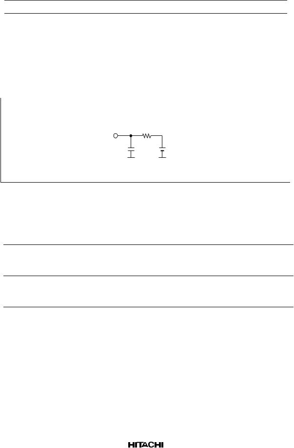
Output Load
Dout 500Ω
50 pF* 1.4 V
(Including scope & jig)
Read Cycle
|
|
HM62V256 |
|
|
|
|
|
|
|
|
|
-7 |
|
-8 |
|
-10 |
|
|
|
Parameter |
Symbol |
Min |
Max |
Min |
Max |
Min |
Max |
Unit |
Notes |
|
|
|
|
|
|
|
|
|
|
Read cycle time |
tRC |
70 |
— |
85 |
— |
100 |
— |
ns |
|
Address access time |
tAA |
— |
70 |
— |
85 |
— |
100 |
ns |
|
Chip select access time |
tACS |
— |
70 |
— |
85 |
— |
100 |
ns |
|
Output enable to output valid |
tOE |
— |
35 |
— |
45 |
— |
50 |
ns |
|
Chip selection to output in low-Z |
tCLZ |
10 |
— |
10 |
— |
10 |
— |
ns |
2 |
Output enable to output in low-Z |
tOLZ |
5 |
— |
5 |
— |
5 |
— |
ns |
2 |
Chip deselection to output in high-Z |
tCHZ |
0 |
25 |
0 |
30 |
0 |
35 |
ns |
1, 2 |
Output disable to output in high-Z |
tOHZ |
0 |
25 |
0 |
30 |
0 |
35 |
ns |
1, 2 |
Output hold from address change |
tOH |
10 |
— |
10 |
— |
10 |
— |
ns |
|
Notes: 1. tCHZ and tOHZ are defined as the time at which the outputs achieve the open circuit conditions and are not referred to output voltage levels.
2. This parameter is sampled and not 100% tested.
7

HM62V256 Series
Read Timing Waveform (1) (WE = VIH)
|
t RC |
Address |
Valid address |
t AA |
|
|
t ACS |
CS |
|
|
t OH |
t OE |
|
|
t OLZ |
OE |
|
|
t OHZ |
|
t CHZ |
High impedance |
|
Dout |
Valid data |
Read Timing Waveform (2) (WE = VIH, CS = VIL, OE = VIL) |
|
|
tRC |
Address |
Valid address |
tAA |
tOH |
tOH |
|
Dout |
Valid data |
Read Timing Waveform (3) (WE = VIH, OE = VIL)*1
|
|
tACS |
CS |
|
|
|
t CLZ |
tCHZ |
Dout |
High impedance |
Valid data |
|
Note: 1. Address must be valid prior to or simultaneously with CS going low.
8

HM62V256 Series
Write Cycle
|
|
HM62V256 |
|
|
|
|
|
|
|
|
|
-7 |
|
-8 |
|
-10 |
|
|
|
Parameter |
Symbol |
Min |
Max |
Min |
Max |
Min |
Max |
Unit |
Notes |
|
|
|
|
|
|
|
|
|
|
Write cycle time |
tWC |
70 |
— |
85 |
— |
100 |
— |
ns |
|
Chip selection to end of write |
tCW |
50 |
— |
75 |
— |
80 |
— |
ns |
4 |
Address setup time |
tAS |
0 |
— |
0 |
— |
0 |
— |
ns |
5 |
Address valid to end of write |
tAW |
50 |
— |
75 |
— |
80 |
— |
ns |
|
Write pulse width |
tWP |
45 |
— |
55 |
— |
60 |
— |
ns |
3, 8 |
Write recovery time |
tWR |
0 |
— |
0 |
— |
0 |
— |
ns |
6 |
Write to output in high-Z |
tWHZ |
0 |
25 |
0 |
30 |
0 |
35 |
ns |
1, 2, 7 |
Data to write time overlap |
tDW |
30 |
— |
35 |
— |
40 |
— |
ns |
|
Data hold from write time |
tDH |
0 |
— |
0 |
— |
0 |
— |
ns |
|
Output active from end of write |
tOW |
10 |
— |
10 |
— |
10 |
— |
ns |
2 |
Output disable to output in high-Z |
tOHZ |
0 |
25 |
0 |
30 |
0 |
35 |
ns |
1, 2, 7 |
Notes: 1. tOHZ and tWHZ are defined as the time at which the outputs achieve the open circuit conditions and are not referred to output voltage levels.
2.This parameter is sampled and not 100% tested.
3.A write occurs during the overlap (tWP) of a low CS and a low WE. A write begins at the later transition of CS going low or WE going low. A write ends at the earlier transition ofCS going high or WE going high. tWP is measured from the beginning of write to the end of write.
4.tCW is measured from CS going low to the end of write.
5.tAS is measured from the address valid to the beginning of write.
6.tWR is measured from the earlier of WE or CS going high to the end of write cycle.
7.During this period, I/O pins are in the output state so that the input signals of the opposite phase to the outputs must not be applied.
8.In the write cycle with OE low fixed, tWP must satisfy the following equation to avoid a problem of data bus contention, tWP ³ tWHZ max + tDW min.
9

HM62V256 Series
Write Timing Waveform (1) (OE Clock)
|
t WC |
|
|
Address |
Valid address |
|
|
|
|
||
|
t AW |
|
t WR |
OE |
|
|
|
|
t CW |
|
|
CS |
|
|
|
|
*1 |
|
|
|
t AS |
t WP |
|
WE |
|
|
|
|
t OHZ |
|
|
Dout |
|
High impedance |
|
|
|
|
|
|
|
t DW |
t DH |
Din |
High impedance |
Valid data |
|
|
|||
Notes: 1. If CS goes low simultaneously with WE going low or after WE going low, the outputs remain in the high impedance state.
10