

motorola / 74AC4020
.PDF14 Stage Binary Ripple Counter
The MC74AC4020 consists of 14 master-slave flip-flops with 12 stages brought out to pins. The output of each flip-flop feeds the next and the frequency at each output is half that of the preceding one. The state of the counter advances on the negative-going edge of the Clock input. Reset is asynchronous and active-high.
State changes of the Q outputs do not occur simultaneously because of internal ripple delays. Therefore, decoded output signals are subject to decoding spikes and may have to be gated with the Clock of the MC74AC4020 for some designs.
•140 MHz Typ. Clock
•Outputs Source/Sink 24 mA
•Operating Voltage Range: 2.0 to 6.0 V
•High Noise Immunity
VCC |
Q11 |
|
Q10 |
|
Q8 |
|
Q9 |
RESET CLK |
|
Q1 |
||||||
|
16 |
|
15 |
|
14 |
|
13 |
|
12 |
|
11 |
|
10 |
|
9 |
|
|
|
|
|
|
|
|
|
|
|
|
|
|
|
|
|
|
|
|
|
|
|
|
|
|
|
|
|
|
|
|
|
|
|
|
|
|
|
|
|
|
|
|
|
|
|
|
|
|
|
|
1 |
|
2 |
|
3 |
|
4 |
|
5 |
|
6 |
|
7 |
|
8 |
Q12 |
Q13 |
|
Q14 |
|
Q6 |
|
Q5 |
|
Q7 |
Q4 |
GND |
|||
FUNCTION TABLE
Clock |
Reset |
Output State |
||
|
|
|
|
|
|
|
|
L |
No Change |
|
|
|
||
|
|
|
|
|
|
|
|
L |
Advance to next state |
|
|
|
||
X |
H |
All Outputs are low |
||
|
|
|
|
|
MC74AC4020
14-STAGE
BINARY RIPPLE
COUNTER
N SUFFIX
CASE 648-08
PLASTIC
D SUFFIX
CASE 751B-05
PLASTIC
LOGIC DIAGRAM
|
|
|
|
|
|
9 |
|
Q1 |
|
|
|
|
|
|
7 |
|
|
|
|
|
|
|
|
|
Q4 |
|
|
|
|
|
|
|
|
|
|
|
|
|
|
|
|
5 |
||
|
|
|
|
|
|
|
Q5 |
|
|
|
|
|
|
|
|
|
|
|
|
|
|
|
|
4 |
||
|
|
|
|
|
|
|
Q6 |
|
10 |
|
|
|
|
|
|||
|
|
|
6 |
|||||
|
|
|
|
Q7 |
||||
CLOCK |
|
|
|
|
|
|
||
|
|
13 |
||||||
|
|
|
|
|
|
|
Q8 |
|
|
|
|
|
|
|
|
|
|
|
|
|
|
|
|
12 |
||
|
|
|
|
|
|
|
Q9 |
|
|
|
|
|
|
|
|
|
|
|
|
|
|
|
|
14 |
||
|
|
|
|
|
|
|
Q10 |
|
|
|
|
|
|
|
|
|
|
|
|
|
|
|
|
15 |
||
|
|
|
|
|
|
|
Q11 |
|
|
|
|
|
|
|
|
|
|
|
|
|
|
|
|
1 |
||
|
|
|
|
|
|
|
Q12 |
|
|
|
|
|
|
|
|
|
|
|
|
|
|
|
|
2 |
||
|
|
|
|
|
|
|
Q13 |
|
|
|
|
|
|
|
|
|
|
|
|
|
|
|
|
3 |
|
|
|
|
|
|
|
|
|
Q14 |
|
11 |
|
|
|
|
|
|||
|
|
|
|
|
||||
|
|
|
|
|
|
|||
|
|
|
|
|
|
|||
RESET |
|
|
|
|
|
|
|
|
|
|
|
|
|
|
|
||
PIN 16 = VCC |
|
|
|
|
||||
PIN 8 = GND |
|
|
|
|
||||
FACT DATA
5-1
MC74AC4020
MAXIMUM RATINGS*
Symbol |
Parameter |
Value |
Unit |
|
|
|
|
VCC |
DC Supply Voltage (Referenced to GND) |
±0.5 to +7.0 |
V |
Vin |
DC Input Voltage (Referenced to GND) |
±0.5 to VCC +0.5 |
V |
Vout |
DC Output Voltage (Referenced to GND) |
±0.5 to VCC +0.5 |
V |
Iin |
DC Input Current, per Pin |
±20 |
mA |
Iout |
DC Output Current, per Pin |
±50 |
mA |
ICC |
DC VCC or GND Current per Output Pin |
±50 |
mA |
PD |
Power Dissipation in Still Air |
750 |
mW |
|
Plastic** |
|
|
|
SOIC Package** |
500 |
|
|
|
|
|
Tstg |
Storage Temperature |
±65 to +150 |
°C |
TL |
Lead Temperature, 1 mm from Case for 10 seconds |
260 |
°C |
|
(Plastic DIP or SOIC Package) |
|
|
|
|
|
|
* Maximum Ratings are those values beyond which damage to the device may occur. ** Derating: Plastic DIP: ± 10mW/°C from 65°C to 125°C
SOIC Package: ±7.0 mW/°C from 65°C to 125°C
RECOMMENDED OPERATING CONDITIONS
Symbol |
|
Parameter |
Min |
Max |
Unit |
|
|
|
|
|
|
|
|
VCC |
DC Supply Voltage (Referenced to GND) |
|
2.0 |
6.0 |
V |
|
Vin/Vout |
Input Voltage, Output Voltage (Ref. to GND) |
0 |
VCC |
|
||
TA |
Operating Temperature, All Package Types |
±40 |
+85 |
°C |
||
tr/tf |
Input Rise/Fall Time |
VCC = 3.0 |
V |
0 |
150 |
ns/V |
|
(Figure 1) |
VCC = 4.5 |
V |
0 |
40 |
|
|
|
VCC = 5.5 |
V |
0 |
25 |
|
FACT DATA
5-2

MC74AC4020
DC CHARACTERISTICS (unless otherwise specified)
Symbol |
Parameter |
Value |
Unit |
|
|
|
|
|
|
|
|
|
|
Vin = VCC or GND |
ICC |
Maximum Quiescent Supply Voltage |
80 |
μA |
VCC = 5.5 V, |
|
|
|
|
TA = Worst Case |
|
|
|
|
Vin = VCC or GND |
ICC |
Maximum Quiescent Supply Current |
8.0 |
μA |
VCC = 5.5 V, |
|
|
|
|
TA = 25°C |
DC CHARACTERISTICS
|
|
|
74AC |
74AC |
|
|
|
|
|
|
|
|
|
|
|
|
|
Symbol |
Parameter |
VCC |
TA = +25°C |
TA = |
Unit |
|
Conditions |
|
(V) |
±40°C to +85°C |
|
||||||
|
|
|
|
|
|
|
|
|
|
|
|
Typ |
Guaranteed Limits |
|
|
|
|
|
|
|
|
|
|
|
|
|
VIH |
Minimum High Level |
3.0 |
|
2.1 |
2.1 |
|
VOUT = 0.1 V |
|
|
Input Voltage |
4.5 |
|
3.15 |
3.15 |
V |
or VCC ± 0.1 V |
|
|
|
5.5 |
|
3.85 |
3.85 |
|
|
|
|
|
|
|
|
|
|
|
|
VIL |
Maximum Low Level |
3.0 |
|
0.9 |
0.9 |
|
VOUT = 0.1 V |
|
|
Input Voltage |
4.5 |
|
1.35 |
1.35 |
V |
or VCC ± 0.1 V |
|
|
|
5.5 |
|
1.65 |
1.65 |
|
|
|
|
|
|
|
|
|
|
|
|
VOH |
Minimum High Level |
3.0 |
2.99 |
2.9 |
2.9 |
|
IOUT = ±50 μA |
|
|
Output Voltage |
4.5 |
4.49 |
4.4 |
4.4 |
V |
|
|
|
|
5.5 |
5.49 |
5.4 |
5.4 |
|
|
|
|
|
|
|
|
|
|
|
|
|
|
|
|
|
|
|
*VIN = VIL or VIH |
|
|
|
3.0 |
|
2.56 |
2.46 |
V |
|
±12 mA |
|
|
4.5 |
|
3.86 |
3.76 |
IOH |
±24 mA |
|
|
|
|
|
|||||
|
|
5.5 |
|
4.86 |
4.76 |
|
|
±24 mA |
|
|
|
|
|
|
|
|
|
VOL |
Maximum Low Level |
3.0 |
0.002 |
0.1 |
0.1 |
|
IOUT = 50 μA |
|
|
Output Voltage |
4.5 |
0.001 |
0.1 |
0.1 |
V |
|
|
|
|
5.5 |
0.001 |
0.1 |
0.1 |
|
|
|
|
|
|
|
|
|
|
|
|
|
|
|
|
|
|
|
*VIN = VIL or VIH |
|
|
|
3.0 |
|
0.36 |
0.44 |
V |
|
12 mA |
|
|
4.5 |
|
0.36 |
0.44 |
IOL |
24 mA |
|
|
|
|
|
|||||
|
|
5.5 |
|
0.36 |
0.44 |
|
|
24 mA |
|
|
|
|
|
|
|
|
|
IIN |
Maximum Input |
|
|
± |
± |
μ |
|
|
|
Leakage Current |
5.5 |
|
0.1 |
1.0 |
A |
VI = VCC, GND |
|
IOLD |
Minimum Dynamic |
5.5 |
|
|
75 |
mA |
VOLD = 1.65 V Max |
|
|
Output Current** |
|
|
|
|
|
|
|
IOHD |
5.5 |
|
|
±75 |
mA |
VOHD = 3.85 V Min |
||
|
|
|
||||||
*All outputs loaded; thresholds on input associated with output under test.
**Maximum test duration 2.0 ms, one output loaded at a time.
FACT DATA
5-3
MC74AC4020
AC CHARACTERISTICS (For Figures and Waveforms Ð See Section 3)
|
|
|
|
|
|
74AC |
|
74AC |
|
|
||
|
|
|
|
|
|
|
|
|
|
|
|
|
|
|
|
VCC* |
|
TA = +25°C |
|
TA = ±40°C |
|
Fig. |
|||
Symbol |
|
Parameter |
|
|
to +85°C |
Unit |
||||||
|
(V) |
|
CL = 50 pF |
|
No. |
|||||||
|
|
|
|
|
CL = 50 pF |
|
||||||
|
|
|
|
|
|
|
|
|
|
|
||
|
|
|
|
Min |
|
Typ |
|
Max |
Min |
Max |
|
|
|
|
|
|
|
|
|
|
|
|
|
|
|
fmax |
Maximum Clock |
3.3 |
110 |
|
0 |
|
|
100 |
|
MHz |
|
|
Frequency |
5.0 |
130 |
|
140 |
|
|
120 |
|
|
|||
|
|
|
|
|
|
|
||||||
|
|
|
|
|
|
|
|
|
|
|
|
|
tPLH |
Propagation Delay |
3.3 |
2.0 |
|
|
|
11 |
2.0 |
14 |
ns |
|
|
CP to Q1 |
|
5.0 |
2.0 |
|
|
|
8.0 |
2.0 |
10 |
|
||
|
|
|
|
|
|
|
||||||
|
|
|
|
|
|
|
|
|
|
|
|
|
tPHL |
Propagation Delay |
3.3 |
2.0 |
|
|
|
11 |
2.0 |
14 |
ns |
|
|
CP to Q1 |
|
5.0 |
2.0 |
|
|
|
8.0 |
2.0 |
10 |
|
||
|
|
|
|
|
|
|
||||||
|
|
|
|
|
|
|
|
|
|
|
|
|
tPLH |
Propagation Delay |
3.3 |
2.0 |
|
|
|
18 |
2.0 |
21 |
ns |
|
|
CP to Q4 |
|
5.0 |
2.0 |
|
|
|
13 |
2.0 |
16 |
|
||
|
|
|
|
|
|
|
||||||
|
|
|
|
|
|
|
|
|
|
|
|
|
tPHL |
Propagation Delay |
3.3 |
2.0 |
|
|
|
18 |
2.0 |
21 |
ns |
|
|
CP to Q4 |
|
5.0 |
2.0 |
|
|
|
13 |
2.0 |
16 |
|
||
|
|
|
|
|
|
|
||||||
|
|
|
|
|
|
|
|
|
|
|
|
|
tPHL |
Propagation Delay |
3.3 |
3.0 |
|
|
|
12 |
3.0 |
15 |
ns |
|
|
Reset to any Q |
5.0 |
3.0 |
|
|
|
10 |
3.0 |
12 |
|
|||
|
|
|
|
|
|
|||||||
|
|
|
|
|
|
|
|
|
|
|
|
|
tPHL |
Propagation Delay |
3.3 |
0 |
|
|
|
5.5 |
0 |
6.5 |
ns |
|
|
On to Qn |
+1 |
5.0 |
0 |
|
|
|
3.5 |
0 |
4.5 |
|
||
|
|
|
|
|
|
|||||||
tPHL |
Propagation Delay |
3.3 |
0 |
|
|
|
5.5 |
0 |
6.5 |
ns |
|
|
On to Qn |
+1 |
5.0 |
0 |
|
|
|
3.5 |
0 |
4.5 |
|
||
|
|
|
|
|
|
|||||||
trec |
Recovery Time |
3.3 |
0 |
|
±2.5 |
|
|
0 |
|
ns |
|
|
MR to CP |
5.0 |
0 |
|
±1.5 |
|
|
0 |
|
|
|||
|
|
|
|
|
|
|
|
|||||
|
|
|
|
|
|
|
|
|
|
|
|
|
tw CP |
Minimum Pulse Width |
3.3 |
4.0 |
|
3.5 |
|
|
4.5 |
|
ns |
|
|
Clock Pin |
|
5.0 |
3.0 |
|
2.5 |
|
|
3.5 |
|
|
||
|
|
|
|
|
|
|
|
|||||
|
|
|
|
|
|
|
|
|
|
|
|
|
tw MR |
Minimum Pulse Width |
3.3 |
4.0 |
|
3.5 |
|
|
4.5 |
|
ns |
|
|
Master Reset |
5.0 |
3.0 |
|
2.5 |
|
|
3.5 |
|
|
|||
|
|
|
|
|
|
|
||||||
|
|
|
|
|
|
|
|
|
|
|
|
|
*Voltage Range 3.3 V is 3.3 V ±0.3 V. Voltage Range 5.0 V is 5.0 V ±0.5 V.
CAPACITANCE
Symbol |
Parameter |
Value |
Unit |
Test Conditions |
|
Typ |
|||||
|
|
|
|
||
|
|
|
|
|
|
CIN |
Input Capacitance |
4.5 |
pF |
VCC = 5.0 V |
|
CPD |
Power Dissipation Capacitance |
50 |
pF |
VCC = 5.0 V |
FACT DATA
5-4
MC74AC4020
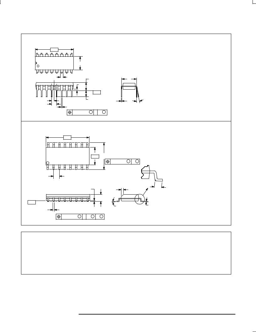
OUTLINE DIMENSIONS
N SUFFIX
PLASTIC DIP PACKAGE ±A± CASE 648±08
ISSUE R
16 |
|
|
9 |
|
|
|
|
|
B |
|
|
1 |
|
|
8 |
|
|
|
|
F |
C |
|
L |
|
|
|
|
||
|
|
|
S |
|
|
|
|
|
±T± |
SEATING |
|
|
|
|
|
PLANE |
|
|
H |
|
K |
J |
M |
|
G |
|
|
||
|
|
|
|
|
|
|
|
D 16 PL |
|
|
|
|
|
|
0.25 (0.010) M T A |
M |
|
NOTES:
1.DIMENSIONING AND TOLERANCING PER ANSI Y14.5M, 1982.
2.CONTROLLING DIMENSION: INCH.
3.DIMENSION L TO CENTER OF LEADS WHEN FORMED PARALLEL.
4.DIMENSION B DOES NOT INCLUDE MOLD FLASH.
5.ROUNDED CORNERS OPTIONAL.
|
INCHES |
MILLIMETERS |
||
DIM |
MIN |
MAX |
MIN |
MAX |
A |
0.740 |
0.770 |
18.80 |
19.55 |
B |
0.250 |
0.270 |
6.35 |
6.85 |
C |
0.145 |
0.175 |
3.69 |
4.44 |
D |
0.015 |
0.021 |
0.39 |
0.53 |
F |
0.040 |
0.70 |
1.02 |
1.77 |
G |
0.100 BSC |
2.54 BSC |
||
H |
0.050 BSC |
1.27 BSC |
||
J |
0.008 |
0.015 |
0.21 |
0.38 |
K |
0.110 |
0.130 |
2.80 |
3.30 |
L |
0.295 |
0.305 |
7.50 |
7.74 |
M |
0 |
10 |
0 |
10 |
S |
0.020 |
0.040 |
0.51 |
1.01 |
|
|
D SUFFIX |
|
|
|
PLASTIC SOIC PACKAGE |
|
±A± |
|
CASE 751B±05 |
|
|
|
ISSUE J |
|
16 |
9 |
|
|
|
±B± |
P 8 PL |
|
1 |
8 |
0.25 (0.010) M B |
S |
G |
|
|
|
|
K |
|
F |
|
R X 45_ |
||
|
|
C |
|
±T± SEATING |
|
M |
J |
PLANE |
|
||
|
|
|
|
D 16 PL |
|
|
|
0.25 (0.010) M |
T B S A |
S |
|
NOTES:
1.DIMENSIONING AND TOLERANCING PER ANSI Y14.5M, 1982.
2.CONTROLLING DIMENSION: MILLIMETER.
3.DIMENSIONS A AND B DO NOT INCLUDE MOLD PROTRUSION.
4.MAXIMUM MOLD PROTRUSION 0.15 (0.006) PER SIDE.
5.DIMENSION D DOES NOT INCLUDE DAMBAR PROTRUSION. ALLOWABLE DAMBAR PROTRUSION SHALL BE 0.127 (0.005) TOTAL IN EXCESS OF THE D DIMENSION AT MAXIMUM MATERIAL CONDITION.
|
MILLIMETERS |
INCHES |
||
DIM |
MIN |
MAX |
MIN |
MAX |
A |
9.80 |
10.00 |
0.386 |
0.393 |
B |
3.80 |
4.00 |
0.150 |
0.157 |
C |
1.35 |
1.75 |
0.054 |
0.068 |
D |
0.35 |
0.49 |
0.014 |
0.019 |
F |
0.40 |
1.25 |
0.016 |
0.049 |
G |
1.27 BSC |
0.050 BSC |
||
J |
0.19 |
0.25 |
0.008 |
0.009 |
K |
0.10 |
0.25 |
0.004 |
0.009 |
M |
0 |
7 |
0 |
7 |
P |
5.80 |
6.20 |
0.229 |
0.244 |
R |
0.25 |
0.50 |
0.010 |
0.019 |
Motorola reserves the right to make changes without further notice to any products herein. Motorola makes no warranty, representation or guarantee regarding the suitability of its products for any particular purpose, nor does Motorola assume any liability arising out of the application or use of any product or circuit, and specifically disclaims any and all liability, including without limitation consequential or incidental damages. ªTypicalº parameters can and do vary in different applications. All operating parameters, including ªTypicalsº must be validated for each customer application by customer's technical experts. Motorola does not convey any license under its patent rights nor the rights of others. Motorola products are not designed, intended, or authorized for use as components in systems intended for surgical implant into the body, or other applications intended to support or sustain life, or for any other application in which the failure of the Motorola product could create a situation where personal injury or death may occur. Should Buyer purchase or use Motorola products for any such unintended or unauthorized application, Buyer shall indemnify and hold Motorola and its officers, employees, subsidiaries, affiliates, and distributors harmless against all claims, costs, damages, and expenses, and reasonable attorney fees arising out of, directly or indirectly, any claim of personal injury or death associated with such unintended or unauthorized use, even if such claim alleges that Motorola was negligent regarding the design or manufacture of the part. Motorola and  are registered trademarks of Motorola, Inc. Motorola, Inc. is an Equal Opportunity/Affirmative Action Employer.
How to reach us: |
|
USA/EUROPE: Motorola Literature Distribution; |
JAPAN: Nippon Motorola Ltd.; Tatsumi±SPD±JLDC, Toshikatsu Otsuki, |
P.O. Box 20912; Phoenix, Arizona 85036. 1±800±441±2447 |
6F Seibu±Butsuryu±Center, 3±14±2 Tatsumi Koto±Ku, Tokyo 135, Japan. 03±3521±8315 |
MFAX: RMFAX0@email.sps.mot.com ±TOUCHTONE (602) 244±6609 |
HONG KONG: Motorola Semiconductors H.K. Ltd.; 8B Tai Ping Industrial Park, |
INTERNET: http://Design±NET.com |
51 Ting Kok Road, Tai Po, N.T., Hong Kong. 852±26629298 |
◊ MC74AC4020/D
*MC74AC4020/D*