

motorola / 6n135
.pdfFEATURES
•Isolation Test Voltage: 2500 VACRMS
•TTL Compatible
•High Bit Rates: 1 Mbit/s
•High Common-Mode Interference Immunity
•Bandwidth 2 MHz
•Open-Collector Output
•External Base Wiring Possible
•Field-Effect Stable by TRIOS*
•Underwriters Lab File #E52744
DESCRIPTION
The 6N135 and 6N136 are optocouplers with a GaAIAs infrared emitting diode, optically coupled with an integrated photodetector which consists of a photodiode and a high-speed transistor in a DIP- 8 plastic package.
Signals can be transmitted between two electrically separated circuits up to frequencies of 2 MHz. The potential difference between the circuits to be coupled is not allowed to exceed the maximum permissible reference voltages.
Maximum Ratings |
|
|
Emitter |
|
|
Reverse Voltage ................................................. |
5 |
V |
Forward Current ............................................ |
25 mA |
|
Peak Forward Current |
|
|
(t =1 ms, duty cycle 50%) ............................ |
50 mA |
|
Maximum Surge Forward Current |
|
|
(t ≤1 µs, 300 pulses/s)....................................... |
1 A |
|
Thermal Resistance................................... |
700 K/W |
|
Total Power Dissipation (TA≤70°C) ............... |
45 mW |
|
Detector |
|
|
Supply Voltage ..................................... |
–0.5 to 15 |
V |
Output Voltage .................................... |
–0.5 to 15 |
V |
Emitter-Base Voltage ......................................... |
5 |
V |
Output Current................................................. |
8 mA |
|
Maximum Output Current.............................. |
16 mA |
|
Base Current .................................................. |
5 mA |
|
Thermal Resistance................................... |
300 K/W |
|
Total Power Dissipation (TA≤70°C) ............. |
100 mW |
|
Package
Isolation Test Voltage (between emitter and detector climate per DIN 40046,
part 2, Nov. 74 (t=1min.) ............... |
2500 VACRMS |
||
Pollution Degree (DIN VDE 0109) ......................... |
2 |
||
Creepage ........................................................... |
|
≥7 mm |
|
Clearance........................................................... |
|
≥7 mm |
|
Comparative Tracking Index per |
|
||
DIN IEC112/VDE 0303 part 1, |
|
||
Group IIIa per DIN VDE 6110 ........................ |
175 |
||
Isolation Resistance |
≥1012 Ω |
||
V |
=500 V, T |
= 25°C ............................... |
|
IO |
A |
= 100°C |
≥1011 Ω |
V |
=500 V, T |
||
IO |
A |
|
–55°C to +125°C |
Storage Temperature Range ....... |
|||
Ambient Temperature Range ...... |
–55°C to +100°C |
||
Soldering Temperature (max. ≤10 sec., |
|||
dip soldering ≥0.5 mm from |
260°C |
||
case bottom).............................................. |
|
||
*TRIOS—TRansparent IOn Shield
|
|
|
|
|
|
|
|
6N135 |
|
|
|
|
|
|
|
|
6N136 |
|
|
|
HIGH-SPEED 2.5 kV TRIOS |
|||||
|
|
|
|
|
|
|
OPTOCOUPLER |
|
Dimensions in inches (mm) |
|
|
|
|
|
|
|
|
4 |
3 |
2 |
1 |
Pin |
|
|
|
|
|
|
|
|
One |
|
|
|
|
|
|
|
|
I.D. |
NC |
1 |
8 |
Cathode |
|
|
|
|
|
(VCC) |
|||
|
|
|
|
|
|
|
|
|
.268 (6.81) |
|
|
|
|
Anode |
2 |
7 |
Base |
|
|
|
|
(VB) |
||||
.255 (6.48) |
|
|
|
|
|
|
|
|
|
|
|
|
Cathode |
3 |
6 |
Collector |
|
|
|
|
|
(VO) |
||||
|
|
|
|
|
NC |
4 |
5 |
Emitter |
5 |
6 |
7 |
8 |
|
|
|
|
(GND) |
|
|
|
|
|
||||
|
.390 (9.91) |
|
|
|
|
|
|
|
|
.379 (9.63) |
|
|
|
|
|
|
|
|
.045 (1.14) |
|
|
|
|
|
.305 typ. |
|
|
|
|
|
|
|
(7.75) typ. |
|
|
|
.030 (.76) |
|
|
|
|
|
|
|
|
.150 (3.81) |
|
|
.130 (3.30) |
.135 (3.43) |
|
|
|
4° |
|
.115 (2.92) |
.040 (1.02) |
10° |
|
Typ. |
.030 (.76 ) |
Typ. |
.022 (.56) |
|
3°–9° .012 (.30) |
.018 (.46) |
.100 (2.54) |
.008 (.20) |
|
||
|
|
|
|
Typ. |
|
Characteristics (T =0 to 70°C unless otherwise specified, T=25°C typ.) |
||||
A |
|
|
|
A |
Emitter |
Symbol |
|
Unit |
Condition |
|
|
|
|
|
Forward Voltage |
VF |
1.6 (≤1.9) |
V |
IF=16 mA |
Breakdown Voltage |
VBR |
≥5 |
V |
IR=10 µA |
Reverse Current |
IR |
0.5 (≤10) |
µA |
VR=5 V |
Capacitance |
CO |
125 |
pF |
VR=0 V, f=1 MHz |
Temperature Coeffi- |
VF / TA |
-1.7 |
mV/°C |
IF=16 mA |
cient, Forward Voltage |
||||
|
|
|
|
|
Detector |
|
|
|
|
|
|
|
|
|
Supply Current |
|
|
µA |
IF=16 mA, VO open, |
Logic Low |
ICCL |
150 |
VCC=15 V |
|
Supply Current |
|
0.01 (≤1) |
µA |
IF=0 mA, VO open, |
Logic High |
ICCH |
VCC=15 V |
||
Output Voltage, |
|
|
|
IF=16 mA, |
Output Low |
|
0.1 (≤0.4) |
|
VCC=4.5 V |
6N135 |
VOL |
V |
IO=1.1 mA |
|
6N136 |
VOL |
0.1 (≤0.4) |
V |
IO=2.4 mA |
Output Current, |
|
3 (≤500) |
|
|
Output High |
ICH |
nA |
IF=0 mA, |
|
|
|
|
|
VO=VCC=5.5 V |
Output Current, |
|
0.01 (≤1) |
µA |
IF=0 mA |
Output High |
ICH |
VO=VCC=15 V |
||
Current Gain |
HFE |
150 |
|
VO=5 V, IO=3 mA |
Package |
|
|
|
|
|
|
|
|
|
Coupling Capacitance |
|
|
|
|
Input-Output |
CIO |
0.6 |
pF |
f=1 MHz |
Current Transfer Ratio |
|
|
|
|
|
|
|
|
|
6N135 |
CTR |
16 (≥7) |
% |
IF=16 mA, VO=0.4 V, |
6N136 |
CTR |
35 (≥19) |
% |
VCC=4.5 V, TA=25°C |
6N135 |
CTR |
≥5 |
% |
IF=16 mA, VO=0.5 V, |
6N136 |
CTR |
≥15 |
|
VCC=4.5 V |
5–1 |
|
|
|
|
This document was created with FrameMaker 4.0.4
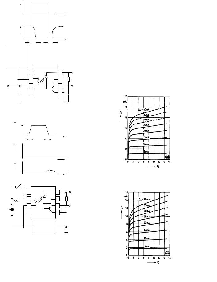
Figure 1. Switching times
IF |
|
|
|
t |
|
VO |
5 V |
|
|
||
VOL |
1.5 V |
|
t |
||
|
||
tPHL |
tPLH |
Pulse generator
ZO=50 Ω tr,tf=5 ns
duty cycle 10% t≤100 s
IF
IF Monitor
 100 Ω
100 Ω
1 |
8 |
5 V |
2 |
7 |
RL |
3 |
6 |
VO |
4 |
5 |
CL |
|
|
|
|
|
15 pF |
Figure 2. Common-mode interference immunity
VCM |
|
|
|
|
|
|
|
|
|
|
|
|
|
|
|
|
|
|||||||
|
10 V |
90% |
|
|
|
|
|
|
|
|
|
|
|
10% |
|
|
|
|||||||
|
|
|
|
|
|
|
|
|
|
|
|
|
|
|
||||||||||
|
|
|
|
|
|
|
|
|
|
|
|
|
|
|||||||||||
|
|
|
|
|
|
|
|
|
|
|
|
|
|
|||||||||||
|
0 V |
|
10% |
|
|
|
|
|
|
|
|
|
|
|
|
|
|
|
|
90% |
|
|
||
|
|
|
|
|
|
|
|
|
|
|
|
|||||||||||||
|
|
|
|
|
|
|
|
|
|
|
|
|
|
|
|
|
|
|
|
|
|
|
|
|
|
|
|
|
tr |
|
|
|
|
|
|
|
tf |
|
|
|
|
|
|
t |
|||||
|
|
|
|
|
|
|
|
|
|
|
|
|
|
|
|
|
|
|
||||||
|
|
|
|
|
|
|
|
|
|
|
|
|
|
|
|
|
|
|
||||||
|
|
|
|
|
|
|
|
|
|
|
|
|
|
|
|
|
|
|
|
|||||
VO |
|
|
|
|
|
|
|
|
|
|
|
|
|
|
|
|
|
|||||||
5 V 
A: IF=0 mA
t
VO
VOL |
|
B: IF=16 mA |
||
|
|
t |
||
|
|
|
||
IF |
1 |
8 |
5 V |
|
A |
2 |
7 |
RL |
|
B |
3 |
6 |
VO |
|
VFF |
||||
4 |
5 |
|
||
|
|
|||
+V Pulse generator CM ZO=50 Ω
tr,tf=8 ns
Delay Time (IF=16 mA, VCC=5 V, TA=25°C)
High - Low |
|
|
|
|
|
|
6N135 (RL=4.1 kΩ) |
tPHL |
0.3 (≤1.5) |
|
µs |
|
|
6N136 (RL=1.9 kΩ) |
tPHL |
0.2 (≤0.8) |
|
µs |
|
|
Low - High |
|
|
|
|
|
|
6N135 (RL=4.1 kΩ) |
tPLH |
0.3 (≤1.5) |
|
µs |
|
|
6N136 (RL=1.9 kΩ) |
tPLH |
0.2 (≤0.8) |
|
µs |
|
|
Common Mode Interference Immunity |
|
|
|
|||
(VCM=10 VP-P, VCC=5 V, TA=25°C) |
|
|
|
|
||
High (IF=0 mA) |
|
|
|
|
|
|
6N135 (RL=4.1 kΩ) |
CMH |
|
1000 |
V/µs |
|
|
6N136 (RL=1.9 kΩ) |
CMH |
|
1000 |
V/µs |
|
|
Low (IF=16 mA) |
|
|
|
|
|
|
6N135 (RL=4.1 kΩ) |
CML |
|
1000 |
V/µs |
|
|
6N136 (RL=1.9 kΩ) |
CML |
|
1000 |
V/µs |
|
|
Figure 3. Output characteristics-6N135 Output current versus output voltage
(TA=25°C, VCC=5 V)
Figure 4. Output characteristics-6N136 Output current versus output voltage
(TA=25°C, VCC=5 V)
6N135/136
5–2
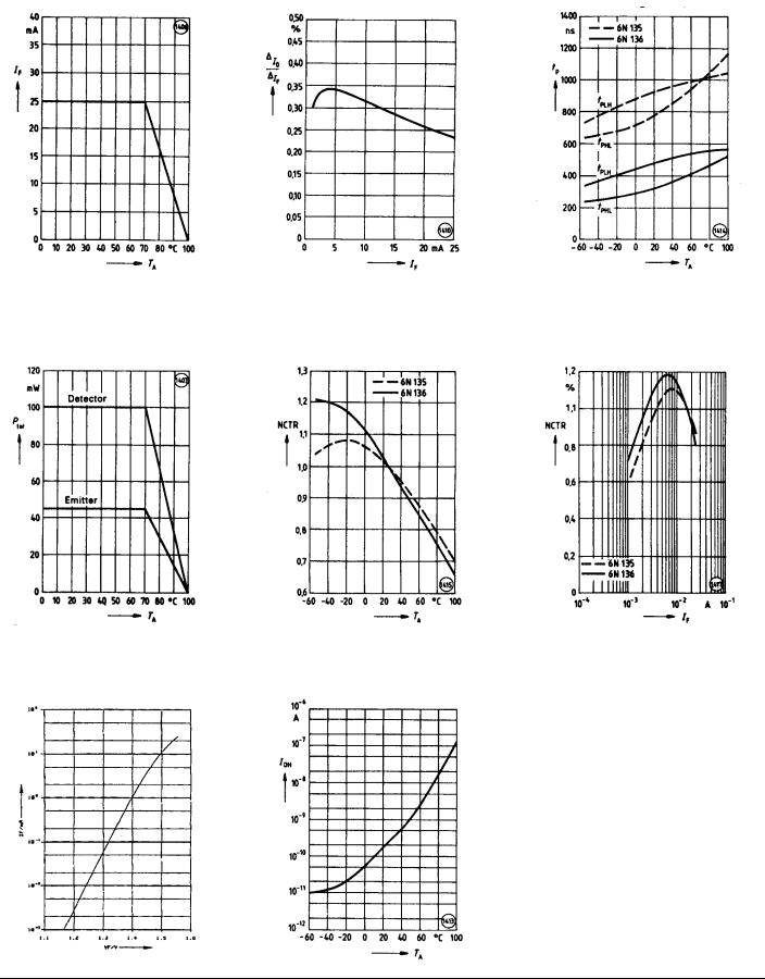
Figure 5. Permissible forward current of emitting diode versus ambient temperature
Figure 6. Permissible total power dissipation versus ambient temperature
Figure 7. Forward current of emitting diodeversus forward voltage (TA=25°C)
Figure 8. Small signal transfer ratio versus forward current (VCC=5 V, TA=25°C)
Figure 9. Current transfer ratio (normalized) versus ambient temperature (nor-
malized to IF=16 mA, VO=0.4 V, VCC=5 V, TA=25°C)
Figure 10. Output current (high)versus ambient temperature
(VO=VCC=5 V, IF=0)
Figure 11. Delay times versus ambient temperature (IF=16 mA, VCC=5 V, 6N135: RL=4.1 kΩ, 6N136: RL=1.9 kΩ)
Figure 12. Current transfer ratio (normalized) versus forward current
(IF=16 mA, VO=0.4 V, VCC=5 V, TA=25°C)
6N135/136
5–3