

motorola / 4HC4060A
.PDFMOTOROLA
SEMICONDUCTOR TECHNICAL DATA
14-Stage Binary Ripple
Counter With Oscillator
High±Performance Silicon±Gate CMOS
The MC54/74C4060A is identical in pinout to the standard CMOS MC14060B. The device inputs are compatible with standard CMOS outputs; with pullup resistors, they are compatible with LSTTL outputs.
This device consists of 14 master±slave flip±flops and an oscillator with a frequency that is controlled either by a crystal or by an RC circuit connected externally. The output of each flip±flop feeds the next and the frequency at each output is half of that of the preceding one. The state of the counter advances on the negative±going edge of the Osc In. The active±high Reset is asynchronous and disables the oscillator to allow very low power consumption during stand±by operation.
State changes of the Q outputs do not occur simultaneously because of internal ripple delays. Therefore, decoded output signals are subject to decoding spikes and may have to be gated with Osc Out 2 of the HC4060A.
•Output Drive Capability: 10 LSTTL Loads
•Outputs Directly Interface to CMOS, NMOS, and TTL
•Operating Voltage Range: 2 to 6 V
•Low Input Current: 1 μA
•High Noise Immunity Characteristic of CMOS Devices
•In Compliance With JEDEC Standard No. 7A Requirements
•Chip Complexity: 390 FETs or 97.5 Equivalent Gates
LOGIC DIAGRAM
|
Osc Out 1 |
Osc Out 2 |
|
|||||
|
|
10 |
|
9 |
|
|
||
|
|
|
|
|
|
|
Q4 |
|
|
|
|
|
|
|
|
7 |
|
|
|
|
|
|
|
|
5 |
|
|
|
|
|
|
|
|
Q5 |
|
|
11 |
|
|
|
|
|
4 |
|
Osc In |
|
|
|
|
|
Q6 |
||
|
|
|
|
|
|
6 |
||
|
|
|
|
|
|
|
Q7 |
|
|
|
|
|
|
|
|
14 |
|
|
|
|
|
|
|
|
Q8 |
|
|
|
|
|
|
|
|
13 |
|
|
|
|
|
|
|
|
Q9 |
|
|
|
|
|
|
|
|
15 |
|
|
|
|
|
|
|
|
Q10 |
|
|
|
|
|
|
|
|
1 |
|
|
|
|
|
|
|
|
Q12 |
|
|
|
|
|
|
|
|
2 |
|
|
|
|
|
|
|
|
Q13 |
|
|
|
|
|
|
|
|
3 |
|
|
|
|
|
|
|
|
Q14 |
|
|
12 |
|
|
|
|
|
|
|
|
|
|
|
|
|
|
||
Reset |
|
|
|
|
Pin 16 = VCC |
|||
|
|
|
|
|
Pin 8 = GND |
|||
|
|
|
|
|
|
|||
MC54/74HC4060A
|
|
J SUFFIX |
16 |
CERAMIC PACKAGE |
|
CASE 620±10 |
||
1 |
|
|
|
|
N SUFFIX |
16 |
PLASTIC PACKAGE |
|
1 |
CASE 648±08 |
|
|
|
|
|
|
D SUFFIX |
16 |
SOIC PACKAGE |
|
1 |
CASE 751B±05 |
|
|
|
|
|
|
DT SUFFIX |
16 |
TSSOP PACKAGE |
|
1 |
CASE 748C±03 |
|
ORDERING INFORMATION |
||
MC54HCXXXXAJ |
Ceramic |
|
MC74HCXXXXAN |
Plastic |
|
MC74HCXXXXAD |
SOIC |
|
MC74HCXXXXADT |
TSSOP |
|
FUNCTION TABLE
Clock |
Reset |
Output State |
||||
|
|
|
|
|
|
|
|
|
|
|
|
L |
No Charge |
|
|
|
|
|
||
|
|
|
|
|
L |
Advance to Next State |
|
|
|
|
|
||
|
X |
H |
All Outputs Are Low |
|||
|
|
|
|
|
|
|
Pinout: 16±Lead Plastic Package (Top View)
|
|
|
|
|
|
|
|
|
|
|
|
|
|
|
Osc |
|
Osc |
||
VCC |
Q10 |
|
Q8 |
|
Q9 |
Reset |
Osc In |
Out 1 |
Out 2 |
||||||||||
|
16 |
|
15 |
|
14 |
|
13 |
|
12 |
|
|
11 |
|
|
10 |
|
|
9 |
|
|
|
|
|
|
|
|
|
|
|
|
|
|
|
|
|
|
|
|
|
|
|
|
|
|
|
|
|
|
|
|
|
|
|
|
|
|
|
|
|
|
|
|
|
|
|
|
|
|
|
|
|
|
|
|
|
|
|
|
|
1 |
|
2 |
|
3 |
|
4 |
|
5 |
|
6 |
|
7 |
|
8 |
Q12 |
Q13 |
|
Q14 |
|
Q6 |
|
Q5 |
|
Q7 |
Q4 |
GND |
|||
3/96
Motorola, Inc. 1996 |
REV 1 |

MC54/74HC4060A
MAXIMUM RATINGS*
Symbol |
Parameter |
Value |
Unit |
|
|
|
|
|
|
VCC |
DC Supply Voltage (Referenced to GND) |
± 0.5 to + 7.0 |
V |
|
Vin |
DC Input Voltage (Referenced to GND) |
± 0.5 to VCC + 0.5 |
V |
|
Vout |
DC Output Voltage (Referenced to GND) |
± 0.5 to VCC + 0.5 |
V |
|
Iin |
DC Input Current, per Pin |
± 20 |
mA |
|
Iout |
DC Output Current, per Pin |
± 25 |
mA |
|
ICC |
DC Supply Current, VCC and GND Pins |
± 50 |
mA |
|
PD |
Power Dissipation in Still Air, Plastic or Ceramic DIP² |
750 |
mW |
|
|
SOIC Package² |
500 |
|
|
|
TSSOP Package² |
450 |
|
|
|
|
|
|
|
Tstg |
Storage Temperature Range |
± 65 to + 150 |
_C |
|
TL |
Lead Temperature, 1 mm from Case for 10 Seconds |
|
_C |
|
|
Plastic DIP, SOIC or TSSOP Package |
260 |
|
|
|
Ceramic DIP |
300 |
|
|
|
|
|
|
This device contains protection circuitry to guard against damage due to high static voltages or electric fields. However, precautions must be taken to avoid applications of any voltage higher than maximum rated voltages to this high±impedance circuit. For proper operation, Vin and
Vout should be constrained to the
range GND v (Vin or Vout) v VCC. Unused inputs must always be
tied to an appropriate logic voltage level (e.g., either GND or VCC). Unused outputs must be left open.
*Maximum Ratings are those values beyond which damage to the device may occur. Functional operation should be restricted to the Recommended Operating Conditions.
²Derating Ð Plastic DIP: ± 10 mW/ _C from 65_ to 125_C
Ceramic DIP: ± 10 mW/_C from 100_ to 125_C
SOIC Package: ± 7 mW/_C from 65_ to 125_C TSSOP Package: ± 6.1 mW/_C from 65_ to 125_C
For high frequency or heavy load considerations, see Chapter 2 of the Motorola High±Speed CMOS Data Book (DL129/D).
RECOMMENDED OPERATING CONDITIONS
Symbol |
Parameter |
|
Min |
Max |
Unit |
|
|
|
|
|
|
VCC |
DC Supply Voltage (Referenced to GND) |
|
2.5* |
6.0 |
V |
Vin, Vout |
DC Input Voltage, Output Voltage (Referenced to GND) |
0 |
VCC |
V |
|
TA |
Operating Temperature Range, All Package Types |
± 55 |
+ 125 |
_C |
|
tr, tf |
Input Rise/Fall Time |
VCC = 2.0 V |
0 |
1000 |
ns |
|
(Figure 1) |
VCC = 4.5 V |
0 |
500 |
|
|
|
VCC = 6.0 V |
0 |
400 |
|
*The oscillator is guaranteed to function at 2.5 V minimum. However, parametrics are tested at 2.0 V by driving Pin 11 with an external clock source.
DC CHARACTERISTICS (Voltages Referenced to GND)
|
|
|
|
VCC |
Guaranteed Limit |
|
|
||
|
|
|
|
|
|
|
|
|
|
Symbol |
Parameter |
Condition |
V |
±55 to 25°C |
≤85°C |
≤125°C |
Unit |
||
|
|
|
|
|
|
|
|
|
|
VIH |
Minimum High±Level Input Voltage |
Vout = 0.1V or VCC ±0.1V |
2.0 |
1.50 |
1.50 |
|
1.50 |
V |
|
|
|
|Iout| ≤ 20μA |
|
3.0 |
2.10 |
2.10 |
|
2.10 |
|
|
|
|
|
4.5 |
3.15 |
3.15 |
|
3.15 |
|
|
|
|
|
6.0 |
4.20 |
4.20 |
|
4.20 |
|
|
|
|
|
|
|
|
|
|
|
VIL |
Maximum Low±Level Input Voltage |
Vout = 0.1V or VCC ± 0.1V |
2.0 |
0.50 |
0.50 |
|
0.50 |
V |
|
|
|
|Iout| ≤ 20μA |
|
3.0 |
0.90 |
0.90 |
|
0.90 |
|
|
|
|
|
4.5 |
1.35 |
1.35 |
|
1.35 |
|
|
|
|
|
6.0 |
1.80 |
1.80 |
|
1.80 |
|
|
|
|
|
|
|
|
|
|
|
VOH |
Minimum High±Level Output |
Vin = VIH or VIL |
|
2.0 |
1.9 |
1.9 |
|
1.9 |
V |
|
Voltage (Q4±Q10, Q12±Q14) |
|Iout| ≤ 20μA |
|
4.5 |
4.4 |
4.4 |
|
4.4 |
|
|
|
|
|
6.0 |
5.9 |
5.9 |
|
5.9 |
|
|
|
|
|
|
|
|
|
|
|
|
|
Vin =VIH or VIL |
|Iout| ≤ 2.4mA |
3.0 |
2.48 |
2.34 |
|
2.20 |
|
|
|
|
|Iout| ≤ 4.0mA |
4.5 |
3.98 |
3.84 |
|
3.70 |
|
|
|
|
|Iout| ≤ 5.2mA |
6.0 |
5.48 |
5.34 |
|
5.20 |
|
MOTOROLA |
3±2 |

MC54/74HC4060A
DC CHARACTERISTICS (Voltages Referenced to GND)
|
|
|
|
VCC |
Guaranteed Limit |
|
||
|
|
|
|
|
|
|
|
|
Symbol |
Parameter |
Condition |
V |
±55 to 25°C |
≤85°C |
≤125°C |
Unit |
|
|
|
|
|
|
|
|
|
|
VOL |
Maximum Low±Level Output |
Vin = VIH or VIL |
|
2.0 |
0.1 |
0.1 |
0.1 |
V |
|
Voltage (Q4±Q10, Q12±Q14) |
|Iout| ≤ 20μA |
|
4.5 |
0.1 |
0.1 |
0.1 |
|
|
|
|
|
6.0 |
0.1 |
0.1 |
0.1 |
|
|
|
|
|
|
|
|
|
|
|
|
Vin = VIH or VIL |
|Iout| ≤ 2.4mA |
3.0 |
0.26 |
0.33 |
0.40 |
|
|
|
|
|Iout| ≤ 4.0mA |
4.5 |
0.26 |
0.33 |
0.40 |
|
|
|
|
|Iout| ≤ 5.2mA |
6.0 |
0.26 |
0.33 |
0.40 |
|
VOH |
Minimum High±Level Output |
Vin = VCC or GND |
|
2.0 |
1.9 |
1.9 |
1.9 |
V |
|
Voltage (Osc Out 1, Osc Out 2) |
|Iout| ≤ 20μA |
|
4.5 |
4.4 |
4.4 |
4.4 |
|
|
|
|
|
6.0 |
5.9 |
5.9 |
5.9 |
|
|
|
|
|
|
|
|
|
|
|
|
Vin =VCC or GND |
|Iout| ≤ 0.7mA |
3.0 |
2.48 |
2.34 |
2.20 |
|
|
|
|
|Iout| ≤ 1.0mA |
4.5 |
3.98 |
3.84 |
3.70 |
|
|
|
|
|Iout| ≤ 1.3mA |
6.0 |
5.48 |
5.34 |
5.20 |
|
VOL |
Maximum Low±Level Output |
Vin = VCC or GND |
|
2.0 |
0.1 |
0.1 |
0.1 |
V |
|
Voltage (Osc Out 1, Osc Out 2) |
|Iout| ≤ 20μA |
|
4.5 |
0.1 |
0.1 |
0.1 |
|
|
|
|
|
6.0 |
0.1 |
0.1 |
0.1 |
|
|
|
|
|
|
|
|
|
|
|
|
Vin =VCC or GND |
|Iout| ≤ 0.7mA |
3.0 |
0.26 |
0.33 |
0.40 |
|
|
|
|
|Iout| ≤ 1.0mA |
4.5 |
0.26 |
0.33 |
0.40 |
|
|
|
|
|Iout| ≤ 1.3mA |
6.0 |
0.26 |
0.33 |
0.40 |
|
Iin |
Maximum Input Leakage Current |
Vin = VCC or GND |
|
6.0 |
±0.1 |
±1.0 |
±1.0 |
μA |
ICC |
Maximum Quiescent Supply |
Vin = VCC or GND |
|
6.0 |
4 |
40 |
160 |
μA |
|
Current (per Package) |
Iout = 0μA |
|
|
|
|
|
|
NOTE: Information on typical parametric values can be found in Chapter 2 of the Motorola High±Speed CMOS Data Book (DL129/D).
AC CHARACTERISTICS (CL = 50 pF, Input tr = tf = 6 ns)
|
|
VCC |
Guaranteed Limit |
|
|
||
|
|
|
|
|
|
|
|
Symbol |
Parameter |
V |
±55 to 25°C |
≤85°C |
|
≤125°C |
Unit |
|
|
|
|
|
|
|
|
fmax |
Maximum Clock Frequency (50% Duty Cycle) |
2.0 |
6.0 |
9.0 |
|
8.0 |
MHz |
|
(Figures 1 and 4) |
3.0 |
10 |
14 |
|
12 |
|
|
|
4.5 |
30 |
28 |
|
25 |
|
|
|
6.0 |
50 |
45 |
|
40 |
|
|
|
|
|
|
|
|
|
tPLH, |
Maximum Propagation Delay, Osc In to Q4* |
2.0 |
300 |
375 |
|
450 |
ns |
tPHL |
(Figures 1 and 4) |
3.0 |
180 |
200 |
|
250 |
|
|
|
4.5 |
60 |
75 |
|
90 |
|
|
|
6.0 |
51 |
64 |
|
75 |
|
|
|
|
|
|
|
|
|
tPLH, |
Maximum Propagation Delay, Osc In to Q14* |
2.0 |
500 |
750 |
|
1000 |
ns |
tPHL |
(Figures 1 and 4) |
3.0 |
350 |
450 |
|
600 |
|
|
|
4.5 |
250 |
275 |
|
300 |
|
|
|
6.0 |
200 |
220 |
|
250 |
|
|
|
|
|
|
|
|
|
tPHL |
Maximum Propagation Delay, Reset to Any Q |
2.0 |
195 |
245 |
|
300 |
ns |
|
(Figures 2 and 4) |
3.0 |
75 |
100 |
|
125 |
|
|
|
4.5 |
39 |
49 |
|
61 |
|
|
|
6.0 |
33 |
42 |
|
53 |
|
|
|
|
|
|
|
|
|
tPLH, |
Maximum Propagation Delay, Qn to Qn+1 |
2.0 |
75 |
95 |
|
125 |
ns |
tPHL |
(Figures 3 and 4) |
3.0 |
60 |
75 |
|
95 |
|
|
|
4.5 |
15 |
19 |
|
24 |
|
|
|
6.0 |
13 |
16 |
|
20 |
|
|
|
|
|
|
|
|
|
3±3 |
MOTOROLA |

MC54/74HC4060A
AC CHARACTERISTICS (CL = 50 pF, Input tr = tf = 6 ns) ± continued
|
|
VCC |
Guaranteed Limit |
|
|
||
|
|
|
|
|
|
|
|
Symbol |
Parameter |
V |
±55 to 25°C |
≤85°C |
|
≤125°C |
Unit |
|
|
|
|
|
|
|
|
tTLH, |
Maximum Output Transition Time, Any Output |
2.0 |
75 |
95 |
|
110 |
ns |
tTHL |
(Figures 1 and 4) |
3.0 |
27 |
32 |
|
36 |
|
|
|
4.5 |
15 |
19 |
|
22 |
|
|
|
6.0 |
13 |
16 |
|
19 |
|
|
|
|
|
|
|
|
|
Cin |
Maximum Input Capacitance |
|
10 |
10 |
|
10 |
pF |
NOTE: For propagation delays with loads other than 50 pF, and information on typical parametric values, see Chapter 2 of the Motorola High± Speed CMOS Data Book (DL129/D).
* For TA = 25°C and CL = 50 pF, typical propagation delay from Clock to other Q outputs may be calculated with the following equations:
VCC = 2.0 |
V: tP = [93.7 + 59.3 (n±1)] ns |
VCC = 4.5 |
V: tP = [30.25 + 14.6 (n±1)] ns |
|
||
VCC = 3.0 |
V: tP = [61.5+ 34.4 (n±1)] ns |
VCC = 6.0 |
V: tP = [24.4 + 12 (n±1)] ns |
|
||
|
|
|
|
|
Typical @ 25°C, VCC = 5.0 V |
|
CPD |
Power Dissipation Capacitance (Per Package)* |
|
|
35 |
pF |
|
*Used to determine the no±load dynamic power consumption: PD = CPD VCC2f + ICC VCC. For load considerations, see Chapter 2 of the Motorola High±Speed CMOS Data Book (DL129/D).
TIMING REQUIREMENTS (Input tr = tf = 6 ns)
|
|
VCC |
Guaranteed Limit |
|
|
||
|
|
|
|
|
|
|
|
Symbol |
Parameter |
V |
±55 to 25°C |
≤85°C |
|
≤125°C |
Unit |
|
|
|
|
|
|
|
|
trec |
Minimum Recovery Time, Reset Inactive to Clock |
2.0 |
100 |
125 |
|
150 |
ns |
|
(Figure 2) |
3.0 |
75 |
100 |
|
120 |
|
|
|
4.5 |
20 |
25 |
|
30 |
|
|
|
6.0 |
17 |
21 |
|
25 |
|
|
|
|
|
|
|
|
|
tw |
Minimum Pulse Width, Clock |
2.0 |
75 |
95 |
|
110 |
ns |
|
(Figure 1) |
3.0 |
27 |
32 |
|
36 |
|
|
|
4.5 |
15 |
19 |
|
23 |
|
|
|
6.0 |
13 |
16 |
|
19 |
|
|
|
|
|
|
|
|
|
tw |
Minimum Pulse Width, Reset |
2.0 |
75 |
95 |
|
110 |
ns |
|
(Figure 2) |
3.0 |
27 |
32 |
|
36 |
|
|
|
4.5 |
15 |
19 |
|
23 |
|
|
|
6.0 |
13 |
16 |
|
19 |
|
|
|
|
|
|
|
|
|
tr, tf |
Maximum Input Rise and Fall Times |
2.0 |
1000 |
1000 |
|
1000 |
ns |
|
(Figure 1) |
3.0 |
800 |
800 |
|
800 |
|
|
|
4.5 |
500 |
500 |
|
500 |
|
|
|
6.0 |
400 |
400 |
|
400 |
|
|
|
|
|
|
|
|
|
NOTE: Information on typical parametric values can be found in Chapter 2 of the Motorola High±Speed CMOS Data Book (DL129/D).
MOTOROLA |
3±4 |
MC54/74HC4060A
PIN DESCRIPTIONS
INPUTS
Osc In (Pin 11)
Negative±edge triggering clock input. A high±to±low transition on this input advances the state of the counter. Osc In may be driven by an external clock source.
Reset (Pin 12)
Active±high reset. A high level applied to this input asynchronously resets the counter to its zero state (forcing all Q outputs low) and disables the oscillator.
OUTPUTS
Q4ÐQ10, Q12±Q14 (Pins 7, 5, 4, 6, 13, 15, 1, 2, 3)
Active±high outputs. Each Qn output divides the Clock input frequency by 2N. The user should note the Q1, Q2, Q3 and Q11 are not available as outputs.
Osc Out 1, Osc Out 2 (Pins 9, 10)
Oscillator outputs. These pins are used in conjunction with Osc In and the external components to form an oscillator (See NO TAG and NO TAG). When Osc In is being driven with an external clock source, Osc Out 1 and Osc Out 2 must be left open circuited. With the crystal oscillator configuration in Figure 6, Osc Out 2 must be left open circuited.
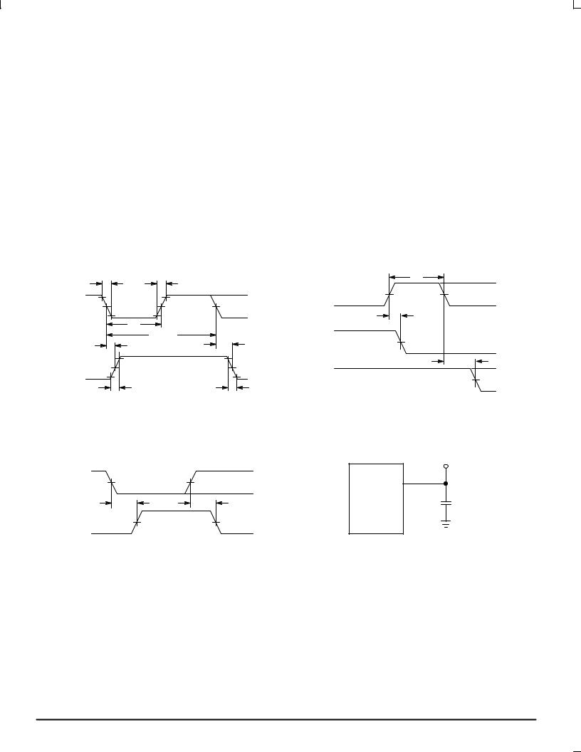
SWITCHING WAVEFORMS
|
tf |
tr |
|
tw |
VCC |
|
|
|
|||
Osc In |
90% |
VCC |
Reset |
50% |
GND |
50% |
|
|
|
||
|
10% |
GND |
|
tPHL |
|
|
tw |
|
|
|
|
|
|
1/fMAX |
Q |
50% |
|
|
tPLH |
tPHL |
|
||
|
|
|
|
||
Q |
90% |
|
|
|
trec |
50% |
|
|
|
VCC |
|
|
|
|
|
||
|
10% |
|
Osc In |
|
50% |
|
tTLH |
tTHL |
|
||
|
|
|
GND |
||
|
|
Figure 1. |
|
Figure 2. |
|
|
|
|
|
|
TEST |
|
|
|
|
|
POINT |
Qn |
|
VCC |
|
OUTPUT |
|
50% |
|
|
|
||
|
|
DEVICE |
|
||
|
|
GND |
|
|
|
|
|
|
UNDER |
|
|
|
tPLH |
tPHL |
|
CL* |
|
|
|
TEST |
|||
Qn+1 |
50% |
|
|
|
|
|
|
|
|
*Includes all probe and jig capacitance |
|
|
|
Figure 3. |
|
Figure 4. Test Circuit |
|
3±5 |
MOTOROLA |

MC54/74HC4060A
Q4 |
Q5 |
Q12 |
Q13 |
Q14 |
7 |
5 |
1 |
2 |
3 |
|
C Q |
|
C Q |
C Q |
C Q |
C Q |
C Q |
|
C Q |
|
C Q |
C Q |
C Q |
C Q |
C |
|
R |
|
R |
|
|
|
|
Osc Out 2 |
9 |
|
|
|
|
|
|
|
|
|
|
|
|
|
|
|
|
Q6 |
= Pin 4 |
|
Q10 = Pin 15 |
|
|
Osc Out 1 |
10 |
Q7 |
= Pin 6 |
|
VCC = Pin 16 |
|
|
|
Q8 |
= Pin 14 |
|
GND = Pin 8 |
|
|
|
|
|
|
|
|
|||
|
|
Q9 |
= Pin 13 |
|
|
|
|
Osc In 11
Reset 12
Figure 5. Expanded Logic Diagram
Reset 12
Osc In 11 Osc Out 1 10 |
Osc Out 2 9 |
 Rtc
Rtc
RS Ctc
For 2.0V ≤ VCC ≤ 6.0V
10Rtc > RS > 2Rtc
400Hz ≤ f ≤ 400Khz:
f [ |
1 |
(f in Hz, R |
in ohms, C in farads) |
|
|||
|
3 RtcCtc |
tc |
tc |
|
|
|
The formula may vary for other frequencies.
Figure 6. Oscillator Circuit Using RC Configuration
Reset 12
Osc In 11 |
Osc Out 1 10 |
9 Osc Out 2 |
|
Rf |
|
|
R1 |
|
C1 |
C2 |
|
Figure 7. Pierce Crystal Oscillator Circuit
MOTOROLA |
3±6 |

MC54/74HC4060A
TABLE 1. CRYSTAL OSCILLATOR AMPLIFIER SPECIFICATIONS (TA = 25°C; Input = Pin 11, Output = Pin 10)
Type |
|
Positive Reactance (Pierce) |
|
|
|
Input Resistance, Rin |
|
60MΩ Minimum |
Output Impedance, Zout (4.5V Supply) |
|
200Ω (See Text) |
Input Capacitance, Cin |
|
5pF Typical |
Output Capacitance, Cout |
|
7pF Typical |
Series Capacitance, Ca |
|
5pF Typical |
Open Loop Voltage Gain with Output at Full Swing, α |
3Vdc Supply |
5.0 Expected Minimum |
|
4Vdc Supply |
4.0 Expected Minimum |
|
5Vdc Supply |
3.3 Expected Minimum |
|
6Vdc Supply |
3.1 Expected Minimum |
|
|
|
PIERCE CRYSTAL OSCILLATOR DESIGN
|
|
RS |
LS |
CS |
|
|
|
|
1 |
2 |
1 |
|
2 |
1 |
Re |
Xe |
2 |
|
|
|
CO |
|
|
|
|
|
|
|
Value are supplied by crystal manufacturer (parallel resonant crystal). |
|
|
|
|
||
Figure 8. Equivalent Crystal Networks
RS |
±jXC2 |
R |
|
|
Rload |
jXLs |
±jXCo |
|
|
Xload |
|
Zload |
±jXC |
|
±jX |
|
|
Cs |
|
|
NOTE: C = C1 + Cin and R = R1 + Rout. Co is considered as part of the load. Ca and Rf typically have minimal effect below 2MHz.
Figure 9. Series Equivalent Crystal Load
Ca
Cin |
Cout |
Values are listed in Table 1.
Figure 10. Parasitic Capacitances of the Amplifier
3±7 |
MOTOROLA |

MC54/74HC4060A
DESIGN PROCEDURES
The following procedure applies for oscillators operating below 2MHz where Z is a resistor R1. Above 2MHz, additional impedance elements should be considered: Cout and Ca of the amp, feedback resistor Rf, and amplifier phase shift error from 180°C.
Step 1: Calculate the equivalent series circuit of the crystal at the frequency of oscillation.
* jXCo(Rs ) jXLs * jXCs)
Ze + * jXCo ) Rs ) jXLs * jXCs + Re ) jXe
Reactance jXe should be positive, indicating that the crystal is operating as an inductive reactance at the oscillation frequency. The maximum Rs for the crystal should be used in the equation.
Step 2: Determine β, the attenuation, of the feedback network. For a closed-loop gain of 2,Aνβ = 2,β = 2/Aν where Aν is the gain of the HC4060A amplifier.
Step 3: Determine the manufacturer's loading capacitance. For example: A manufacturer may specify an external load capacitance of 32pF at the required frequency.
Step 4: Determine the required Q of the system, and calculate Rload, For example, a manufacturer specifies a crystal Q of
100,000. In-circuit Q is arbitrarily set at 20% below crystal Q or 80,000. Then Rload = (2πfoLS/Q) ± Rs where Ls and Rs are crystal parameters.
Step 5: Simultaneously solve, using a computer,
b |
+ |
|
|
|
XC @ XC2 |
|
|
|
|
|
(with feedback phase shift = 180°) |
( Eq 1 ) |
||||||||||
|
|
|
|
|
|
|
|
|
|
|
|
|||||||||||
|
|
R @ Re ) XC2 (Xe * XC) |
|
|
|
|
|
|
|
|
|
|||||||||||
X |
e |
+ X |
C2 |
) X |
C |
) |
ReXC2 |
|
+ X |
Cload |
(where the loading capacitor is an external load, not including C ) |
( Eq 2 ) |
||||||||||
|
||||||||||||||||||||||
|
|
|
|
|
R |
|
|
|
|
|
|
|
|
o |
|
|||||||
|
|
|
|
|
|
|
|
|
|
|
|
|
|
|
|
|
|
|
|
|||
|
|
|
|
RXCoXC2 [(XC ) XC2)(XC ) XCo) * XC(XC ) XCo ) XC2)] |
( Eq 3 ) |
|||||||||||||||||
Rload + |
|
|
|
|
|
|
|
|
|
|
|
|
|
|
|
|
|
|||||
|
|
|
X2 |
(X |
) X |
|
)2 ) R2(X |
C |
) X |
Co ) |
X )2 |
|||||||||||
|
|
|
|
|
|
|
|
|
C2 |
C |
|
|
Co |
|
|
C2 |
|
|||||
Here R = Rout + R1. Rout is amp output resistance, R1 is Z. The C corresponding to XC is given by C = C1 + Cin. Alternately, pick a value for R1 (i.e, let R1 = RS). Solve Equations 1 and 2 for C1 and C2. Use Equation 3 and the fact that Q =
2πfoLs/(Rs + Rload) to find in-circuit Q. If Q is not satisfactory pick another value for R1 and repeat the procedure.
CHOOSING R1
Power is dissipated in the effective series resistance of the crystal. The drive level specified by the crystal manufacturer is the maximum stress that a crystal can withstand without damage or excessive shift in frequency. R1 limits the drive level.
To verify that the maximum dc supply voltage does not overdrive the crystal, monitor the output frequency as a function of voltage at Osc Out 2 (Pin 9). The frequency should increase very slightly as the dc supply voltage is increased. An overdriven crystal will decrease in frequency or become unstable with an increase in supply voltage. The operating supply voltage must be reduced or R1 must be increased in value if the overdriven condition exists. The user should note that the oscillator start-up time is proportional to the value of R1.
SELECTING Rf
The feedback resistor, Rf, typically ranges up to 20MΩ. Rf determines the gain and bandwidth of the amplifier. Proper bandwidth insures oscillation at the correct frequency plus roll-off to minimize gain at undesirable frequencies, such as
the first overtone. Rf must be large enough so as to not affect the phase of the feedback network in an appreciable manner.
ACKNOWLEDGEMENTS AND RECOMMENDED
REFERENCES
The following publications were used in preparing this data sheet and are hereby acknowledged and recommended for reading:
Technical Note TN-24, Statek Corp.
Technical Note TN-7, Statek Corp.
D. Babin, ªDesigning Crystal Oscillatorsº, Machine Design, March 7, 1985.
D. Babin, ªGuidelines for Crystal Oscillator Designº, Machine Design, April 25, 1985.
ALSO RECOMMENDED FOR READING:
E. Hafner, ªThe Piezoelectric Crystal Unit-Definitionsand Method of Measurementº, Proc. IEEE, Vol. 57, No. 2, Feb., 1969.
D. Kemper, L. Rosine, ªQuartz Crystals for Frequency Controlº, Electro-Technology, June, 1969.
P. J. Ottowitz, ªA Guide to Crystal Selectionº, Electronic Design, May, 1966.
MOTOROLA |
3±8 |

MC54/74HC4060A
1 |
2 |
4 |
8 |
16 |
32 |
64 |
128 |
256 |
512 |
1024 |
2048 |
4096 |
8192 |
16384 |
Clock
Reset
Q4
Q5
Q6
Q7
Q8
Q9
Q10
Q12
Q13
Q14
Figure 11. Timing Diagram
3±9 |
MOTOROLA |

MC54/74HC4060A
OUTLINE DIMENSIONS
|
|
|
|
|
|
|
|
|
|
|
|
|
|
|
|
|
|
|
|
|
|
|
|
|
|
|
|
|
|
|
|
|
|
|
|
|
|
|
|
|
|
|
|
|
|
|
|
|
|
J SUFFIX |
|
|
|
|
|
|
|
|
|
|
|
|
|
|
|
|
|
|
|
|
|
|
|
|
|
|
|
|
|
CERAMIC PACKAGE |
|
|
|||||||||||||||||||||||||
|
|
|
|
|
|
|
|
|
|
|
|
|
|
|
|
|
|
±A |
|
|
|
|
|
|
|
|
|
||||||||||||||||||||||||||
|
|
|
|
|
|
|
|
|
|
|
|
|
|
|
|
|
|
|
± |
|
|
|
|
|
|
|
|
|
|
|
|
|
|
|
|
|
|
|
|
|
|
|
|
|
|
|
|
CASE 620±10 |
NOTES: |
||||
|
|
|
|
|
|
|
|
|
|
|
|
|
|
|
|
|
|
|
|
|
|
|
|
|
|
|
|
|
|
|
|
|
|
|
|
|
|
|
|
|
|
|
|
|
|
|
|
|
|
ISSUE V |
|||
16 |
|
|
|
|
|
|
|
|
|
|
|
|
|
9 |
|
|
|
|
|
|
|
|
|
1. |
DIMENSIONING AND TOLERANCING PER |
||||||||||||||||||||||||||||
|
|
|
|
|
|
|
|
|
|
|
|
|
|
|
|
|
|
|
|
|
|
|
|
|
|
|
|
|
|
|
|
|
|
|
|
|
|
|
|
|
|
|
|
|
|
|
|
|
|
|
|
|
ANSI Y14.5M, 1982. |
|
|
|
|
|
|
|
|
|
|
|
|
|
|
|
|
|
|
|
|
|
|
|
|
|
|
|
|
|
|
|
|
|
|
|
|
|
|
|
|
|
|
|
|
±B |
|
|
|
|
2. |
CONTROLLING DIMENSION: INCH. |
|||
1 |
|
|
|
|
|
|
|
|
|
|
|
|
|
8 |
|
|
± |
|
|
|
|
|
|
3. |
DIMENSION L TO CENTER OF LEAD WHEN |
||||||||||||||||||||||||||||
|
|
|
|
|
|
|
|
|
|
|
|
|
|
|
|
|
|
|
|
|
|
|
|
|
FORMED PARALLEL. |
||||||||||||||||||||||||||||
|
|
|
|
|
|
|
|
|
|
|
|
|
|
|
|
|
|
|
|
|
|
|
|
|
|
|
|
|
|
|
|
|
|
|
|
|
|
|
|
|
|
|
|
|
|
C |
|
|
L |
|
4. |
DIM F MAY NARROW TO 0.76 (0.030) WHERE |
|
|
|
|
|
|
|
|
|
|
|
|
|
|
|
|
|
|
|
|
|
|
|
|
|
|
|
|
|
|
|
|
|
|
|
|
|
|
|
|
|
|
|
|
|
|
|
|
|
|
|
THE LEAD ENTERS THE CERAMIC BODY. |
|||
|
|
|
|
|
|
|
|
|
|
|
|
|
|
|
|
|
|
|
|
|
|
|
|
|
|
|
|
|
|
|
|
|
|
|
|
|
|
|
|
|
|
|
|
|
|
|
|
|
|
|
|
|
|
|
|
|
|
|
|
|
|
|
|
|
|
INCHES |
MILLIMETERS |
||
|
|
|
|
|
|
|
|
|
|
|
DIM |
MIN |
MAX |
MIN |
MAX |
±T |
|
|
|
|
|
|
|
|
|
|
A |
0.750 |
0.785 |
19.05 |
19.93 |
|
|
|
|
|
|
|
|
|
|
B |
0.240 |
0.295 |
6.10 |
7.49 |
|
SEATING± |
|
|
N |
|
K |
|
|
|
|
|
C |
Ð |
0.200 |
Ð |
5.08 |
PLANE |
|
|
|
|
|
|
|
|
|
|
D |
0.015 |
0.020 |
0.39 |
0.50 |
|
|
|
|
|
|
|
|
|
|
|
E |
0.050 BSC |
1.27 BSC |
||
|
E |
|
|
|
|
M |
|
|
|
|
F |
0.055 |
0.065 |
1.40 |
1.65 |
|
|
|
|
|
|
|
|
|
G |
0.100 BSC |
2.54 BSC |
||||
F |
G |
|
|
|
|
J 16 PL |
|
|
|
|
J |
0.008 |
0.015 |
0.21 |
0.38 |
|
|
|
|
|
|
|
|
K |
0.125 |
0.170 |
3.18 |
4.31 |
|||
|
|
|
|
|
|
0.25 (0.010) |
|
T |
B |
|
|||||
|
D 16 PL |
|
|
|
|
M |
S |
L |
0.300 BSC |
7.62 BSC |
|||||
|
0.25 (0.010) |
M |
T |
A |
S |
|
|
|
|
|
M |
0° |
15° |
0° |
15° |
|
|
|
|
|
|
N |
0.020 |
0.040 |
0.51 |
1.01 |
|||||
|
|
|
|
N SUFFIX |
|
|
|
±A |
|
PLASTIC PACKAGE |
|
|
|
± |
|
CASE 648±08 |
|
16 |
|
|
9 |
ISSUE R |
|
|
|
|
B |
|
|
1 |
|
|
8 |
|
|
|
|
F |
C |
L |
|
|
|
|
|
||
|
|
|
S |
|
|
|
|
|
±T |
SEATING |
|
|
|
|
± |
PLANE |
|
|
|
|
|
M |
|
|
H |
|
K |
J |
|
|
G |
|
|
||
|
|
|
|
|
|
|
|
D 16 PL |
|
|
|
|
|
|
0.25 (0.010) M T |
A M |
|
NOTES:
1.DIMENSIONING AND TOLERANCING PER ANSI Y14.5M, 1982.
2.CONTROLLING DIMENSION: INCH.
3.DIMENSION L TO CENTER OF LEADS WHEN FORMED PARALLEL.
4.DIMENSION B DOES NOT INCLUDE MOLD FLASH.
5.ROUNDED CORNERS OPTIONAL.
|
INCHES |
MILLIMETERS |
||||
DIM |
MIN |
|
MAX |
MIN |
|
MAX |
A |
0.740 |
|
0.770 |
18.80 |
|
19.55 |
B |
0.250 |
|
0.270 |
6.35 |
|
6.85 |
C |
0.145 |
|
0.175 |
3.69 |
|
4.44 |
D |
0.015 |
|
0.021 |
0.39 |
|
0.53 |
F |
0.040 |
|
0.070 |
1.02 |
|
1.77 |
G |
|
0.100 BSC |
|
2.54 BSC |
||
H |
|
0.050 BSC |
|
1.27 BSC |
||
J |
0.008 |
|
0.015 |
0.21 |
|
0.38 |
K |
0.110 |
|
0.130 |
2.80 |
|
3.30 |
L |
0.295 |
|
0.305 |
7.50 |
|
7.74 |
M |
° |
|
° |
° |
|
° |
|
0 |
|
10 |
0 |
|
10 |
S |
0.020 |
|
0.040 |
0.51 |
|
1.01 |
|
D SUFFIX |
|
PLASTIC SOIC PACKAGE |
±A |
CASE 751B±05 |
± |
ISSUE J |
16 |
9 |
|
|
±B P 8 PL |
|
|
1 |
8 |
± |
0.25 (0.010) M |
B M |
|
||||
|
|
|
G |
|
|
|
K |
|
F |
|
|
° |
||
|
|
R X 45 |
|
|
C |
|
|
±T |
|
J |
|
SEATING± |
M |
||
|
PLANE |
D 16 PL |
|


 0.25 (0.010) M T B S A S
NOTES:
1.DIMENSIONING AND TOLERANCING PER ANSI Y14.5M, 1982.
2.CONTROLLING DIMENSION: MILLIMETER.
3.DIMENSIONS A AND B DO NOT INCLUDE MOLD PROTRUSION.
4.MAXIMUM MOLD PROTRUSION 0.15 (0.006) PER SIDE.
5.DIMENSION D DOES NOT INCLUDE DAMBAR PROTRUSION. ALLOWABLE DAMBAR PROTRUSION SHALL BE 0.127 (0.005) TOTAL IN EXCESS OF THE D DIMENSION AT MAXIMUM MATERIAL CONDITION.
|
MILLIMETERS |
INCHES |
||
DIM |
MIN |
MAX |
MIN |
MAX |
A |
9.80 |
10.00 |
0.386 |
0.393 |
B |
3.80 |
4.00 |
0.150 |
0.157 |
C |
1.35 |
1.75 |
0.054 |
0.068 |
D |
0.35 |
0.49 |
0.014 |
0.019 |
F |
0.40 |
1.25 |
0.016 |
0.049 |
G |
1.27 BSC |
0.050 BSC |
||
J |
0.19 |
0.25 |
0.008 |
0.009 |
K |
0.10 |
0.25 |
0.004 |
0.009 |
M |
0° |
7° |
0° |
7° |
P |
5.80 |
6.20 |
0.229 |
0.244 |
R |
0.25 |
0.50 |
0.010 |
0.019 |
MOTOROLA |
3±10 |